Effect of Net Charge on the Relative Stability of 2D Boron Allotropes
Abstract
We study the effect of electron doping on the bonding character and stability of two-dimensional (2D) structures of elemental boron, called borophene, which is known to form many stable allotropes. Our ab initio calculations for the neutral system reveal previously unknown stable 2D -B and -B structures. We find that the chemical bonding characteristic in this and other boron structures is strongly affected by extra charge. Beyond a critical degree of electron doping, the most stable allotrope changes from -B to a buckled honeycomb structure. Additional electron doping, mimicking a transformation of boron to carbon, causes a gradual decrease in the degree of buckling of the honeycomb lattice that can be interpreted as piezoelectric response. Net electron doping can be achieved by placing borophene in direct contact with layered electrides such as Ca2N. We find that electron doping can be doubled by changing from the B/Ca2N bilayer to the Ca2N/B/Ca2N sandwich geometry.
keywords:
calculation, electronic structure, doping, boron, structural stability, 2DDFT, 2D
Identifying the most stable allotrope of a given compound is one of the key problems in Physics and Chemistry. Whereas charge neutral systems have attracted most attention, notable exceptions are low-dimensional systems that can be charged by doping in specific bulk geometries. Electron doping induced by Li intercalation does not affect the honeycomb structure of two-dimensional (2D) graphene layers in graphite intercalation compounds (GICs) 1, but does change the equilibrium structure of MoS2 monolayers from the 2H to the 1T allotrope 2. Even though the effect of excess charge on chemical bonding and equilibrium geometry should be general, we expect the most drastic changes to occur in structures of elemental boron that is notorious for its many stable allotropes 3, 4. What appears as frustrated bonding in mostly metallic 2D structures of elemental boron, called borophene, reflects the inability of the element to follow the octet rule of bonding due to its electron deficiency. We speculate that both the electron deficiency and thus the chemical bonding characteristic may be modified by placing a nonzero charge on B atoms. In that case, the most stable borophene structure may differ from a puckered triangular lattice with monatomic vacancies 5, 6, 7, 8, 9 or equally stable irregular structures 10, 11, 12 identified in the neutral system. Indeed, placing a net charge of e per atom on borophene, provided by an Al(111) substrate 13, or intercalating Mg ions in-between borophene layers in the MgB2 compound 14, changes the most stable allotrope to a very different honeycomb lattice. Structural changes induced by charging may significantly modify the electronic structure, turning semiconducting 2H-MoS2 to metallic 1T’-MoS2 locally 15 and undoped borophene to honeycomb lattices in diborides 16, 17 including MgB2, which displays superconducting behavior 18.
In this study, we explore the effect of net charge on the bonding character and structural stability of 2D allotropes of boron. Our ab initio calculations for the neutral system reveal a previously unknown stable 2D -B structure with a 0.2 eV wide fundamental band gap. We find that the chemical bonding characteristic in this and other boron structures is strongly affected by extra charge, including a % lattice constant change in -B, induced by changing the net charge from 0.25 holes to 0.25 electrons per B atom. Beyond a critical degree of doping near 0.5 electrons/atom, the most stable allotrope changes from -B to a buckled honeycomb structure. Additional electron doping, mimicking a transformation of boron to carbon, causes a gradual decrease in the degree of buckling of the honeycomb lattice that can be interpreted as piezoelectric response. We propose that net electron doping can easily be achieved by placing borophene in direct contact with layered electrides such as Ca2N. In this system, we find that electron doping of borophene can be doubled by changing from the B/Ca2N bilayer to the Ca2N/B/Ca2N sandwich geometry.
As mentioned above, the vast number of stable neutral 2D borophene allotropes, including B, B, B, B and B structures 5, 6, reflects a frustrated bonding character of electron-deficient boron. This element may engage its three valence electrons in only three covalent bonds, resulting in an electron sextet instead of the desirable octet noble-gas configuration. To partly compensate for lack of electrons in the octet configuration, boron atoms often prefer increasing their coordination to six nearest neighbors in the triangular lattice. This is essentially equivalent to adding electrons 19, 20 to the individual atoms that are held together by pure three-center bonding. On the other hand, the stability of the triangular lattice is often enhanced by removing atoms and forming hexagon-shaped monatomic vacancies. This process somehow mimics subtracting electrons while the structure locally converts to a honeycomb lattice, where atoms are held together by two-center bonding. The competition between two-center and three-center bonding has been used to identify the optimum concentration of hexagonal vacancies in the neutral triangular lattice 21, 19, 22, but likely controls also less common neutral structures with four- and five-fold coordinated boron atoms 10, 11. Biasing this competition by net charge has been shown to affect the fraction of hexagonal vacancies in triangular borophene lattices 23. Even though doping of B layers has been linked to unexpected superconducting behavior of MgB2 and found useful to modulate CO2 capture 24, no systematic attention has been paid to the possibility of deliberately changing the bonding and the equilibrium structure of boron by excess charge.
A viable possibility to significantly dope 2D structures of elemental boron by electrons is to place them in direct contact with electrides including Ca2N 25, 26 and Y2C 27. In these highly electronegative systems with a layered structure, regions of large electron density are found in-between the layers. The charge density in this electron layer amounts to one electron per formula unit in Ca2N and two electrons per formula unit in Y2C. The possibility of exfoliation down to a monolayer 25 has been demonstrated in Ca2N, so that assembly of various vertical heterostructures is possible.
Results
Allotropes of neutral and doped borophene
Inspired by the honeycomb structure of the negatively doped boron sublattice found in diborides including MgB2, we started our investigation of electron doped borophene structures with the honeycomb lattice. To provide substantial configuration freedom for the lattice structure, we consider a superlattice with 32 atoms per unit cell and subject all atoms in the supercell to random distortion. To study the effect of doping on the equilibrium structure and the chemical nature of bonding, we changed the degree of doping gradually and optimized each system using the conjugate gradient optimization method.
| Allotrope | (eV/atom) | ||
| -B | 8 | 4 | |
| -B | 32 | 4, 5, 6 | |
| -B | 8 | 5, 6 | |
| 8 | 5, 6 | ||
| -B | 5 | 3, 5, 6 | |
| 5 | 3, 5, 6 | ||
| -B | 4 | 6 | |
| -B | 4 | 3, 5 | |
| 4 | 3, 5 | ||
| a Present work. | |||
| b Reference [ 3]. | |||
| c Reference [ 8]. |
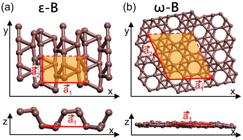
Starting with no excess charge, we found the neutral honeycomb structure to be unstable and to convert to rather stable allotropes that have not been reported previously. The first allotrope, shown in Fig. 1(a) and called -B, is only 7 meV/atom less stable than the most stable -B phase 3 and displays a very uncommon morphology with triangles and pentagons, quite distinct from the well-documented class of triangular lattices with vacancies. The structure shown in Fig. 1(b), which we call -B, has a very similar morphology to known allotropes containing triangles and hexagons only 5, 6, 7, 8, but is meV/atom less stable than -B. -B and -B add to the large number of known allotropes, and we expect many more to follow.
Both -B and -B are buckled. Still, we could locate a locally stable, flat counterpart of -B, which is 7 meV/atom less stable than -B. The cohesive energies of neutral borophene allotropes are compared in Table 1.
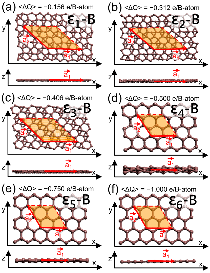
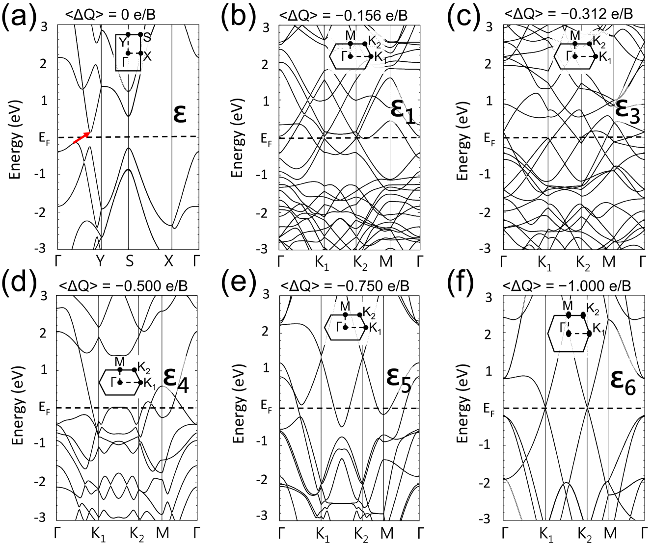
Next, we added extra 5, 10, 13, 16, 24 and 32 electrons to the 32-atom unit cell with an initial honeycomb arrangements and optimized the geometry. We found the optimum geometries not to depend on initial deformations imposed on the starting structure, which may not be reachable in molecular dynamics trajectories. The optimum boron structures labelled and their average doping levels are displayed in Figs. 2(a)-2(f). Optimum structures for different doping levels are discussed in the Supporting Information (SI). We find all these structures to differ significantly from the neutral -B and -B structures in Fig. 1, which have been optimized in the same way.
The structure -B in Fig. 2(a), which contains triangles, pentagons and hexagons, is reminiscent of -B, but is completely flat. With increasing electron doping, the density of pentagons gradually diminishes and eventually vanishes in -B in Fig. 2(c), representing the buckled phase 3. At the same time, the density of hexagons increases from -B to -B until all other polygons are eliminated in , shown in Figs. 2(d)-2(f), as the doping level exceeds e/atom. The buckled honeycomb lattice of -B gradually flattens to the graphene-like structure of -B with increasing electron doping.
The interpretation of these structural changes is rather straight-forward. With one extra electron per atom, boron behaves as -bonded carbon with four valence electrons, with atoms forming the 2D graphene honeycomb lattice. This structure is rather robust with respect to electron and hole doping, as evidenced in GIC structures. Similarly, also doped boron should keep its optimum honeycomb lattice structure even if the net charge may be smaller or larger than one extra electron per atom. As seen in Figs. 2(d)-2(f), the honeycomb structure of borophene, with different degree of buckling, is preferred for the excess charge ranging between and e/atom.
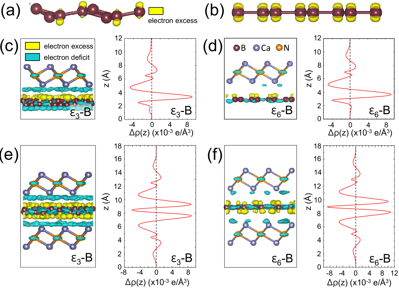
To understand the change in the electronic structure that caused a profound structural change from neutral -B in Fig. 1(a) to negatively charged -B- in Fig. 2(f), we first probed the charge density changes associated with charging. Our results for caused by placing artificially extra electrons on free-standing borophene structures -B and -B are shown in Figs. 3(a)-3(b). can be viewed as the crystal counterpart of the Fukui function, and our results indicate that the extra electrons are accommodated in (or ) states normal to the layer, very similar to graphene layers.
A realistic way to provide a high degree of electron doping, we suggest, is to place borophene layers in contact with the Ca2N electride. The optimum lattice constant of the triangular lattice of Ca2N is Å. This layered system has the nominal configuration [Ca2N]e-, with layers of Ca2N separated by layers of excess electrons, and can be exfoliated down to a monolayer chemically 25. It is to be expected that borophene will be electron doped when placed in the region of excess electrons outside a Ca2N monolayer. Since we focus on general trends rather than minute details, we studied the charge redistribution using only two prototype structures of doped borophene, namely -B at low- and -B at high-level doping, in contact with Ca2N. To determine the degree of electron doping in borophene caused by a contact to Ca2N, we inspected the charge redistribution when placing -B and -B on top of a Ca2N monolayer or, as in a sandwich geometry, in-between Ca2N monolayers. The charge density differences caused by electron redistribution in the system are shown in Figs. 3(c)-3(f). Additional results for -B and -B on top of a [Ca2N]2 bilayer are presented in the SI.
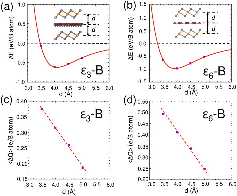
We should point out that incommensurate vertical heterostructures formed of doped borophene and Ca2N layers can not be represented accurately in a periodic structure used in our computational approach. In our calculation, we used the optimum interlayer distance Å in agreement with our results in Figs. 4(a) and 4(b). We furthermore matched -B supercells with Ca2N supercells in the -B/Ca2N superstructure and primitive unit cells of -B with supercells of Ca2N in the -B/Ca2N superstructure. The remaining lattice mismatch of % was accommodated by averaging the lattice constants of borophene and Ca2N. Due to this minor lattice distortion, results presented in Figs. 3(c)-3(f) may differ to a small degree from the charge redistribution in an incommensurate structure. Comparing results for the bilayer in Figs. 3(c)-3(d) with those in the sandwich structure in Figs. 3(e)-3(f), we see clearly that borophene receives twice the number of electrons in the sandwich in comparison to the bilayer structure. Specifically, in -B almost doubles from e/atom in Fig. 3(c) to e/atom in Fig. 3(e). Similarly, in -B almost doubles from e/atom in Fig. 3(d) to e/atom in Fig. 3(f).
We have evaluated the dependence of the total energy on the interlayer distance in the Ca2N/B/Ca2N sandwich structure for the -B and -B allotropes and present our results in Figs. 4(a) and 4(b). In both structures, the optimum interlayer distance Å.
There is a significant electron accumulation with a maximum at Å outside a free-standing Ca2N electride layer 25, which is accommodated by an adjacent borophene layer. In this case, the net charge on the borophene layer may be changed by changing the interlayer distance . Our results for as a function of are presented in Fig. 4(c) for -B and in Fig. 4(d) for -B sandwiched in-between two Ca2N layers. We find it interesting that decreases almost linearly with increasing interlayer distance.
At the equilibrium interlayer distance, we find e/B-atom in the system with -B and e/B-atom in the system with -B. The higher value of in -B is associated with the better ability of this structure to accept electrons.
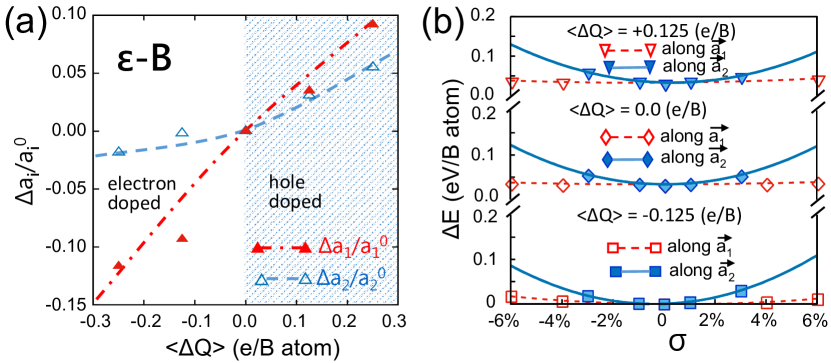
It is well known that in GICs, the net charge transferred from dopant atoms to the graphene layers changes the lattice constant. This change is relatively small, amounting to 28 % in KC8 with e/C-atom. Our corresponding results for the effect of doping on the lattice constants in the stable -B allotrope are shown in Fig. 5(a). The lattice changes are anisotropic and larger than found in graphene. We find that electron doping expands the lattice more along the softer direction than along the harder direction. At the electron doping levels to e/B-atom discussed above for the Ca2N/B/Ca2N heterostructures, the lattice expansion exceeds 10%.
The in-layer stiffness of neutral, electron- and hole-doped -B is addressed in Fig. 5(b). We used the shorthand notation for the neutral system, for e/B and for e/B doping. Irrespective of doping, the energy change due to in-layer strain is much larger along the harder direction than along the softer direction. In terms of the 2D elastic constants 29, we find for the softer direction N/m, N/m, and N/m. Along the harder direction we find N/m, N/m, and N/m.
Electronic structure of borophene allotropes
The electronic band structure of selected boron 2D allotropes discussed in this study is shown in Fig. 6. We should note that DFT calculations used in this study do not represent the true quasi-particle band structure and typically underestimate band gaps. With this fact in mind, we find that, according to the PBE results in Fig. 6(a), the neutral -B allotrope of Fig. 1(a) is a semiconductor with a small indirect band gap of eV. Whereas stretching along the soft direction by 4% turns -B into a direct-gap semiconductor, compressing by 4% along causes gap closure. Stretching -B by 1% along the hard direction turns this allotrope metallic, whereas compression by 1% changes the its indirect gap to a direct gap. More details about the electronic structure of strained -B are provided in the SI.
We find all doped borophene allotropes to be metallic or semi-metallic, as shown in Figs. 6(b)-6(f). Inspection of the band structure reveals the formation of a Dirac cone at K1 and in the honeycomb structures in -B in Fig. 6(e) and in -B in Fig. 6(f). The Dirac cone appears eV above in -B at the doping level e/B and at in -B at e/B, which mimics the structure and valence charge of graphitic carbon.
Discussion
The majority of the reported stable structures of neutral 2D borophene were triangular lattices containing arrays of monatomic vacancies, reflecting the frustrated bonding character of electron-deficient boron. When considering the effect of excess charge on the bonding geometry, we observed a transition driven by increasing net negative charge from structures containing triangles and higher polygons, depicted in Fig. 1(a) and Figs. 2(a)-2(c), for e/B to all-hexagon structures, depicted in Figs. 2(c)-2(f), for e/B. The highest coordinations number of six that may be achieved in a network of triangles reflects to some degree the vain attempt of neutral boron atoms to satisfy the octet rule. Excess negative charge, with the maximum value e/B considered here, offers the ability to satisfy this rule in the honeycomb network of -B in Fig. 2(f).
To understand the chemical origin of these structural changes, we need to inspect the charge redistribution caused by additional doping, corresponding to the Fukui function for a crystal. Corresponding results for in selected electron doped borophene structures are presented in the SI. Complementing our results presented in Fig. 3 for borophene interacting with Ca2N, these results suggest that additional electrons are first accommodated in (or ) states normal to the borophene layer, which cause buckling, and then in states, which reduce the amount of buckling. Starting with the lightly electron doped -B containing triangles, we observe an increasing degree of buckling with increasing electron doping up to e/B. At that point, the structure changes to the honeycomb structure mimicking hole-doped graphene. For e/B, additional excess charge gets increasingly accommodated in states, which are much closer to in borophene than in graphene, causing a reduction of buckling down to zero for e/B.
Assuming that the Ca2N electride can transfer up to one electron per formula unit to a borophene layer, we can expect the maximum average charge per boron atom in B/Ca2N bilayers to range from e in -B/Ca2N to e/atom in -B/Ca2N. The transferred charge may be up to twice as large in Ca2N/B/Ca2N sandwich structures. These values are slightly larger, but close to those found in the actual heterostructures, reported in Fig. 3. We compared the charge transfer between monolayers and multilayers of the Ca2N electride in contact with borophene and found essentially no difference, as seen in the SI. Thus, the number of Ca2N layers does not affect the maximum value of .
It is not easy to achieve the doping level e/B by contacting an electronegative material. According to our results for the Ca2N/B/Ca2N sandwich structure in Fig. 4(d), the Ca2N electride can provide only up to electrons per boron atom, much less than the desired doping level of e/B. An alternative to Ca2N is Y2C, which can supply twice as many electrons as Ca2N, but is hard to exfoliate. Assuming maximum charge transfer from Y2C to borophene, B could receive up to electrons in the Y2C/B/Y2C heterostructure. Such a large electron transfer should further augment the Coulomb attraction between borophene and Y2C, thus further deducing the interlayer distance, as seen in Figs. 3(a) and 3(b), and increase the amount of electron transfer, possibly up to e/B.
We have mentioned electronic structure parallels between the honeycomb structure of -B carrying one extra electron per atom and graphene. Even though the system of electrons near and the Dirac cone in the corner of the Brillouin zone occur in both systems, there are notable differences between the systems. In graphene, the top of the -band lies more than eV below , whereas this energy difference is only eV in -B. Apparently, the lower core charge of elemental boron is the main reason, why the and bands are energetically closer than in graphene. As mentioned before, this results in an increased role of states in electron doped borophene structures.
According to our results in Fig. 5(a), changing the doping level from e to e results in a % increase of the borophene lattice constant . Conversely, we may speculate that changing the lattice constant should modulate the electron transfer from the electride to the borophene layer, thus changing the dipole moment normal to the interface. In that case, an in-plane vibration of the heterostructure will cause this dipole to oscillate and to emit an electromagnetic signal of the same frequency.
Clearly, the most drastic effect of electron doping is seen in the hexagonal borophene structure stabilized in MgB2, which is the cause of superconductivity in this system. Electron doping may also be used as a way to change structures in a predictable way. As an illustration, we find the -B structure 8, which has been synthesized at 680 K on Ag(111), to be very similar to the electron-doped, buckled -B structure. In that case, a simpler way to fabricate -B may consist of bringing borophene in contact with an electride, allowing it to relax to -B while electron doped. The final flat structure of -B may evolve after the electride has been removed. These two examples illustrate new possibilities of using doping to change the structure of boron. Even though doping may have a lesser effect on the equilibrium structure of other systems, our findings about the interplay between structure and excess charge have a general validity.
Summary and Conclusions
In summary, we have studied the effect of electron doping on the bonding character and stability of two-dimensional (2D) structures of elemental boron, called borophene, which is known to form many stable allotropes. Our ab initio calculations for the neutral system have revealed previously unknown stable 2D -B and -B structures in addition to previously reported triangular lattices with monatomic vacancies. We found that the chemical bonding characteristic in this and other boron structures is strongly affected by extra charge, which is first accommodated in the and subsequently in the network of electrons. Beyond a critical degree of electron doping, the most stable allotrope was found to change from -B containing triangles and higher polygons to a buckled honeycomb structure. Additional electron doping, mimicking a transformation of boron to carbon, causes a gradual decrease in the degree of buckling of the honeycomb lattice that can be interpreted as piezoelectric response. We also found that net electron doping can be achieved by placing borophene in direct contact with layered electrides such as Ca2N. We found that electron doping can be doubled to e/B atom by changing from the B/Ca2N bilayer to the Ca2N/B/Ca2N sandwich geometry.
Computational Techniques
Our calculations of the stability, equilibrium structure and electronic structure have been performed using density functional theory (DFT) as implemented in the SIESTA 30 code. Periodic boundary conditions have been used throughout the study, with monolayers represented by a periodic array of slabs separated by a 30 Å thick vacuum region. We used the Perdew-Burke-Ernzerhof (PBE) 31 exchange-correlation functional. The SIESTA calculations used norm-conserving Troullier-Martins pseudopotentials 32, a double- basis including polarization orbitals, and a mesh cutoff energy of Ry to determine the self-consistent charge density, which provided us with a precision in total energy of meV/atom. The reciprocal space has been sampled by a fine grid 33 of -points in the 2D Brillouin zones (BZ) of the primitive unit cells of neutral and doped borophene containing atoms, -points in the BZ of supercell of heterostructure of and , and -points in the BZ of supercell of heterostructure of and . Geometries have been optimized using the conjugate gradient (CG) method 34, until none of the residual Hellmann-Feynman forces exceeded eV/Å.
Additional results are presented for the characterization of borophene layers under conditions not covered in the main manuscript. These include optimum geometries and charge distribution in free-standing electron doped borophene as well as in vertical heterostructures of borophene and Ca2N bilayers. Also presented are electronic band structures of systems described in the main manuscript, results characterizing the effect of strain on the electronic band structure, and charge density differences corresponding to the Fukui function for selected doped borophene allotropes.
Author Information
Corresponding Author
∗E-mail: tomanek@pa.msu.edu
Notes
The authors declare no competing financial interest.
The authors acknowledge financial support by the NSF/AFOSR EFRI 2-DARE grant number EFMA-1433459. We thank Xianqing Lin, Andrii Kyrylchuk and Rick Becker for many enriching discussions. Computational resources have been provided by the Michigan State University High Performance Computing Center.
References
- Dresselhaus and Dresselhaus 1981 Dresselhaus, M. S.; Dresselhaus, G. Adv. Phys. 1981, 30, 139–326
- Py and Haering 1983 Py, M. A.; Haering, R. R. Can. J. Phys. 1983, 61, 76–84
- Wu et al. 2012 Wu, X.; Dai, J.; Zhao, Y.; Zhuo, Z.; Yang, J.; Zeng, X. C. ACS Nano 2012, 6, 7443–7453
- Quandt and Boustani 2005 Quandt, A.; Boustani, I. ChemPhysChem. 2005, 6, 2001–2008
- Evans et al. 2005 Evans, M. H.; Joannopoulos, J. D.; Pantelides, S. T. Phys. Rev. B 2005, 72, 045434
- Kunstmann and Quandt 2006 Kunstmann, J.; Quandt, A. Phys. Rev. B 2006, 74, 035413
- Mannix et al. 2015 Mannix, A. J.; Zhou, X.-F.; Kiraly, B.; Wood, J. D.; Alducin, D.; Myers, B. D.; Liu, X.; Fisher, B. L.; Santiago, U.; Guest, J. R.; Yacaman, M. J.; Ponce, A.; Oganov, A. R.; Hersam, M. C.; Guisinger, N. P. Science 2015, 350, 1513–1516
- Feng et al. 2016 Feng, B.; Zhang, J.; Zhong, Q.; Li, W.; Li, S.; Li, H.; Cheng, P.; Meng, S.; Chen, L.; Wu, K. Nat. Chem. 2016, 8, 563–568
- Zhang et al. 2017 Zhang, Z.; Penev, E. S.; Yakobson, B. I. Chem. Soc. Rev. 2017, 46, 6746–6763
- Zhou et al. 2014 Zhou, X.-F.; Dong, X.; Oganov, A. R.; Zhu, Q.; Tian, Y.; Wang, H.-T. Phys. Rev. Lett. 2014, 112, 085502
- Zhou et al. 2014 Zhou, X.-F.; Oganov, A. R.; Shao, X.; Zhu, Q.; Wang, H.-T. Phys. Rev. Lett. 2014, 113, 176101
- Ma et al. 2016 Ma, F.; Jiao, Y.; Gao, G.; Gu, Y.; Bilic, A.; Chen, Z.; Du, A. Nano Lett. 2016, 16, 3022–3028
- Li et al. 2018 Li, W.; Kong, L.; Chen, C.; Gou, J.; Sheng, S.; Zhang, W.; Li, H.; Chen, L.; Cheng, P.; Wu, K. Sci. Bull. 2018, 63, 282–286
- Nishibori et al. 2001 Nishibori, E.; Takata, M.; Sakata, M.; Tanaka, H.; Muranaka, T.; Akimitsu, J. J. Phys. Soc. Japan 2001, 70, 2252–2254
- Kappera et al. 2014 Kappera, R.; Voiry, D.; Yalcin, S. E.; Branch, B.; Gupta, G.; Mohite, A. D.; Chhowalla, M. Nat. Mater. 2014, 13, 1128
- Perkins 1977 Perkins, P. G. In Boron and Refractory Borides; Matkovich, V., Ed.; Springer: Berlin, 1977; Chapter 3, pp 31–51
- Kolmogorov and Curtarolo 2006 Kolmogorov, A. N.; Curtarolo, S. Phys. Rev. B 2006, 74, 224507
- Nagamatsu et al. 2001 Nagamatsu, J.; Nakagawa, N.; Muranaka, T.; Zenitani, Y.; Akimitsu, J. Nature 2001, 410, 63–64
- Tang and Ismail-Beigi 2007 Tang, H.; Ismail-Beigi, S. Phys. Rev. Lett. 2007, 99, 115501
- Tang and Ismail-Beigi 2009 Tang, H.; Ismail-Beigi, S. Phys. Rev. B 2009, 80, 134113
- Tang and Ismail-Beigi 2010 Tang, H.; Ismail-Beigi, S. Phys. Rev. B 2010, 82, 115412
- Karmodak and Jemmis 2017 Karmodak, N.; Jemmis, E. D. Angew. Chem. Int. Ed. 2017, 56, 10093–10097
- Tarkowski et al. 2018 Tarkowski, T.; Majewski, J. A.; Szwacki, N. G. FlatChem 2018, 7, 42–47
- Tan et al. 2017 Tan, X.; Tahini, H. A.; Smith, S. C. ACS Appl. Mater. Interfaces 2017, 9, 19825–19830
- Druffel et al. 2016 Druffel, D. L.; Kuntz, K. L.; Woomer, A. H.; Alcorn, F. M.; Hu, J.; Donley, C. L.; Warren, S. C. J. Am. Chem. Soc. 2016, 138, 16089–16094
- Lee et al. 2013 Lee, K.; Kim, S. W.; Toda, Y.; Matsuishi, S.; Hosono, H. Nature 2013, 494, 336–340
- Zhang et al. 2014 Zhang, X.; Xiao, Z.; Lei, H.; Toda, Y.; Matsuishi, S.; Kamiya, T.; Ueda, S.; Hosono, H. Chem. Mater. 2014, 26, 6638–6643
- Nixon and Parry 1969 Nixon, D. E.; Parry, G. S. J. Phys. C: Solid State Phys. 1969, 2, 1732–1742
- Liu et al. 2016 Liu, D.; Every, A. G.; Tománek, D. Phys. Rev. B 2016, 94, 165432
- Artacho et al. 2008 Artacho, E.; Anglada, E.; Dieguez, O.; Gale, J. D.; Garcia, A.; Junquera, J.; Martin, R. M.; Ordejon, P.; Pruneda, J. M.; Sanchez-Portal, D.; Soler, J. M. J. Phys. Cond. Mat. 2008, 20, 064208
- Perdew et al. 1996 Perdew, J. P.; Burke, K.; Ernzerhof, M. Phys. Rev. Lett. 1996, 77, 3865–3868
- Troullier and Martins 1991 Troullier, N.; Martins, J. L. Phys. Rev. B 1991, 43, 1993–2006
- Monkhorst and Pack 1976 Monkhorst, H. J.; Pack, J. D. Phys. Rev. B 1976, 13, 5188–5192
- Hestenes and Stiefel 1952 Hestenes, M. R.; Stiefel, E. J. Res. Natl. Bur. Stand. 1952, 49, 409–436