Enhancement of thermoelectric performance of a nanoribbon made of lattice
Abstract
We present electronic and transport properties of a zigzag nanoribbon made of lattice. Our particular focus is on the effects of the continuous evolution of the edge modes ( from flat to dispersive) on the thermoelectric transport properties. Unlike the case of graphene nanoribbon, the zigzag nanoribbon of lattice can host a pair of dispersive (chiral) edge modes at the two valleys for specific width of the ribbon. Moreover, gap opening can also occur at the two valleys depending on the width. The slope of the chiral edge modes and the energy gap strongly depend on the relative strength of two kinds of hoping parameters present in the system. We compute corresponding transport coefficients such as conductance, thermopower, thermal conductance and the thermoelectric figure of merits by using the tight-binding Green function formalism, in order to explore the roles of the dispersive edge modes. It is found that the thermopower and thermoelectric figure of merits can be enhanced significantly by suitably controlling the edge modes. The figure of merits can be enhanced by thirty times under suitable parameter regime in comparison to the case of graphene. Finally, we reveal that the presence of line defect, close to the edge, can cause a significant impact on the edge modes as well as on electrical conductance and thermopower.
I Introduction
The discovery of graphene novo ; neto has boosted the search of graphene-like two-dimensional Dirac materials because of their peculiar band structure and possible technological applications. The electronic properties of Dirac materials are described by the linear band dispersion in low energy regime. The or dice lattice vidal is the graphene-like D material with an additional atom at the centre of hexagon. One of the unique feature of such material is that its quasi particles exhibit higher pseudo spin states vidal unlike in graphene. Apart from it, the additional atom in the lattice causes dispersionless flat band at each valley in addition to the Dirac cones vidal . In recent times, much attention have been paid on such Dirac-Weyl materials with higher spin states, , ,,etc. malcolm ; janik ; lan ; morigi , in order to reveal the roles of the additional atom.
The lattice (pseudo spin ) can be smoothly interpolated to the graphene (pseudo spin ) by using the - model. Here, is related to the strength of the hoping between the central atom to its nearest neighbors and ranges from ‘’ (graphene) to ‘’ (dice lattice or ) lattice. It has recently been shown in Hg1-xCdxTe that this material can be mapped to - model malcolm with under the suitable doping concentration. The continuous evolution from graphene to dice lattice by using model has been extensively exploited in unusual Hall conductivity nicol1 ; tutul1 , Weiss oscillationfiroz_para , Klein tunnelingdaniel ; klein , optical malcolm ; nicol3 ; dora3 ; plasmon ; newT3 properties, irradiation effectsphoto , topological propertiesdora2 and wave packet dynamicstutul2 . However, most of the study of transport properties in the - lattice are limited to the bulk in spite of the fact that electronic band structure as well as the transport phenomena are very sensitive to the edge geometry of honeycomb latticeneto ; newT3 .
The thermoelectric properties of materialnolas have been always under active consideration among research community for its ability to probe the electronic system and potential technological applicationsdisalvo ; snyder . The thermal gradient across the two ends of an electronic system can drive charge carriers from hotter to cooler end and can generate a voltage gradient across these two ends-known as thermopower (S) per unit temperature gradient. Apart from the thermal transport in the bulk of D hexagonal latticedas_sarma ; nam ; hao ; yuri ; wei , several works have demonstrated that thermoelectric performance can be further improved by considering nanoribbon of graphenehossain ; van or black phosphorusMa ; flores .
In this work, we first address the energy band dispersion of the nanoribbon of such material by using tight binding method. Here, we particularly focus on zigzag edge only as it hosts a pair of edge modes. We observe that unlike the case of graphene, the zigzag nanoribbon of exhibits gapless dispersive edge modes (chiral edge modes) for width of ( is the positive integer). On the other hand, the edge modes are gapped for the width . This is in contrast to the case of a zigzag ribbon of grapheneneto where edge modes are dispersionless, gapless and not chiral. Subsequently we use tight-binding Green function approach to obtain the conductance, thermopower and thermoelectric figure of merits of such ribbon. We found that thermopower and figure of merits can be enhanced significantly by controlling the features of edge modes by means of . Finally, we discuss the effects of line defects on edge modes and transport properties.
The paper is organized as follows: In Sec. II, we discuss the tight-binding Hamiltonian and energy band dispersion for zigzag nanoribbon. A brief review of the tight-binding Green function formalism for the evaluation of transport coefficients are presented in Sec. III. In Sec. IV we present our numerical results and discussions. Finally, we summarize our results and conclude in Sec. V.
II Tight binding Hamiltonian and energy dispersion
In this section, we first present a brief description of the lattice geometry of the alpha- lattice. This lattice mimics the geometry of graphene monolayer with an additional atom at the centre of the hexagon. A typical sketch of its hexagon is shown in the Fig (1). It has two different hoping parameters. The hoping parameter between and sublattices is denoted by ‘’ whereas is between the subalttice and .

The tight-binding Hamiltonian of this lattice, without any spin-orbit coupling is given by
| (1) |
where the summation index , and run over , and sublattices. The relevant hoping parameters are and . The creation (annihilation) operators at -th site are denoted by ().
However, we briefly comment here that the Hamiltonian in the continuum model inside the bulk without any boundary can be written in three sublattice space asmorigi
| (2) |
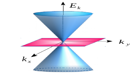
Here, where denotes the two valleys and , respectively. is the D momentum vector and is the Fermi velocity. Note that, the angle is related to the as . The energy dispersion of the above Hamiltonian is linear as , with correspond to band index, as shown in Fig. (2).

It is also worthwhile to mention that the central atom does not play any role in the conic bands except the appearance of dispersionless flat band. However, in presence of magnetic field the C atoms (and hence ) can lift valley degeneracy in the Landau levelsnicol1 ; tutul1 as well as can give rise to the unusual Hall conductivity. This is in contrast to the graphene where the Landau levels at two valleys are identical (degenerate).
In the present study, we particularly focus on such lattice with finite width (nanoribbon), which has not been considered previously in the context of transport.
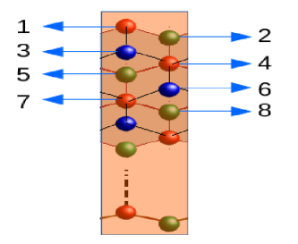

The nanoribbon is considered to be infinitely extended along the -direction with a finite width along the -direction. The nanoribbon can be thought as a linear chain made of iterative unit cells as shown by the rectangular shaped orange shadowed region in Fig. 3. The width of the nanoribbon is given by -the number of atoms per unit cell. To study the transport properties, we consider a two terminal device which consists of three regions as shown in the Fig. (3). The central region is made of zigzag ribbon which is attached to the left and right identical leads. The locations of all the unit cells forming the left and right leads are at and , respectively. Whereas the central regions are composed of the unit cells at . By implementing Bloch’s theorem, total Hamiltonian of the device can be written as
| (3) |
where is the on-site energy matrix of the unit cell at site . On the other hand, or denotes the coupling matrix between the left and right adjacent unit cells. Here, is the unit cell separation. The numbering of atoms in each unit cell is shown in Fig. (4), in order to construct the Hamiltonian matrix. The momentum () along the -direction is conserved as the ribbon is translationally invariant along this direction.

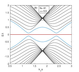
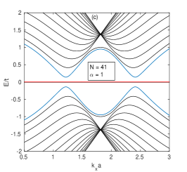
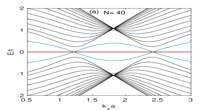
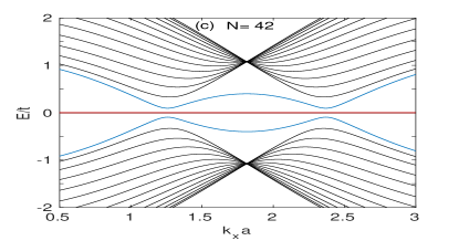
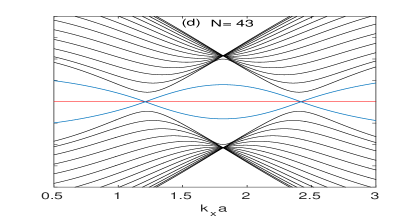
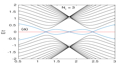
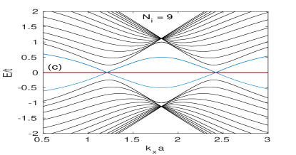
We solve numerically the above equation to obtain the energy dispersion of the nanoribbon and plotted in Fig. (5). We observe that edge modes (sky blue line) can be gapless dispersive or gapped depending on the width. The gapless chiral edge modes appear for the width , otherwise gapped. The hoping parameter between and sublattices are taken corresponding to in both cases. The Fig. (5)a and Fig. (5)d show gapless chiral edge modes for the widths and which satisfy the condition of width and of course both edges are composed of and sublattices only. On the other hand, Fig. (5)b and Fig. (5)c exhibit a pair of gapped edge modes for widths and (i.e., when width ). Note that the crossing of the edge modes for gapless dispersion is the outcome of the additional hoping parameter due to the presence of C sublattices in addition to the usual three nearest neighbor sublattices.
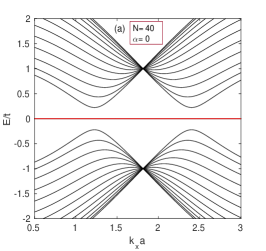
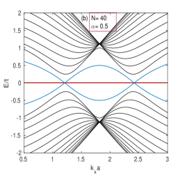
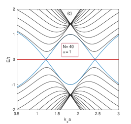
Now we examine how the variation of affects the features of chiral and gapped edge modes. First, we plot the energy dispersion for different values of in Fig. (6). The Fig. (6)a is plotted for and it enforces edge modes to collapse on the dispersionless flat band. Note that the width is corresponding to the case of non-identical edges for i.e, one edge is zigzag and another one is Klein-edge shape as named in Ref. [lakshmi, ]. In such case a gap can be seen between flat band and other transverse modes which is also in agreement with the results based on the Harper equation in Ref. [newT3, ] and analytical work in Ref. [LTP, ]. With the increase of , edge modes emerges and exhibit dispersive feature [see Fig. (6)b] and the slope of which increases further with as shown in Fig. (6)c. This slope actually gives rise to the non-zero group velocity and hence induces significant contribution to the transport properties.
To recover the spectrum of zigzag nanoribbon of graphene, we must make sure that both edges are composed of and sublattices which corresponds to the case of and width . The Fig. (7)a is plotted for these parameters, which shows the dispersionless edge modes as in graphene nanoribbon except the presence of the flat band. Note that the flat band corresponds to the presence of sublattices. We plot the same for in Fig. (7)b which shows that a gap opening occurs between the edge mode and the zero energy flat band. This gap opening increases slowly with the further increase of as shown in Fig. (7)c
III Basic formalism of TB Green function approach
In this section, we discuss the formalism to calculate different transport coefficients under thermal/potential gradient. Let a temperature gradient of is applied between the left and right lead, which induces a voltage gradient . Following the most conventional approach at low temperature regime, the electrical current density and the thermal current density can be written by following Onsager relationonsagar1 ; onsagar2 as
| (4) |
and
| (5) |
where is the electric field and () are the phenomenological transport coefficients which can be expressed in terms of an integral : , with
| (6) |
where and is the Fermi-Dirac distribution function with being the chemical potential. Here, is the energy-dependent transmission amplitude.
Thermopower can be defined under open circuit condition () as dutta ; lv ; groth ; para_th ; Ferrer ; hatef
| (7) |
On the other hand, the electronic contribution to the thermal conductanceFerrer ; hatef can be written as
| (8) |
The thermoelectric performance of a material is quantified by a parameter known as thermoelectric figure of merits and it is given byFerrer ; hatef
| (9) |
Here, is the energy dependent electrical conductance following Landauer-Buttiker formula at non-zero temperature. Here, in the expression of ZT, thermal conductance is taken to be electronic contribution only. The phonon/lattice contribution can be suppressed under very low or very high temperature. One of the key ingredients in all the above equations is the energy dependent transmission probability . In order to obtain for a nanoribbon of this lattice, we shall use the well known tight-binding Green function approach. We first give a brief review of this formalism which was developed by Sanchosancho to study the transfer matrices and spectral density of states at the surface of a semi infinite crystal made of stacked layers. This approach can be used in the hexagonal lattice too, where each supercell acts as independent layer. The method has been already used in several hexagonal lattices like graphenepara , silicenesilicene , Momos2 , phosphorenenjp_ezawa etc. It is also worthwhile to mention at this stage that electron-electron Coulomb interaction can play significant role in nanoribbon geometry which requires many-body Green function GW approximation approachcoulomb or DFT methodDFT and will not be considered here.
Our device is composed of three regions, the central region, the left lead and right lead as shown in Fig. (3). As the left and right leads are identical, we can write and . By implementing transfer matrix approach, the surface Green function can be written as
| (10) |
and
| (11) |
where is identity matrix. The notations and in above two equations can be evaluated as
| (12) |
and
| (13) |
where and are defined as
| (14) |
and
| (15) |
with
| (16) |
and
| (17) |
The summation in Eqs. (12) and (13) has to be taken until and reach to zero. The main advantage of this technique is that unit cells can be captured by just performing iteration. Now we calculate surface Green function by using the following recursion formula
| (18) |
The effects of the left and right leads can be finally incorporated into the total Green function via self energy as
| (19) |
with
| (20) |
and
| (21) |
Now we can define broadening matrix as
| (22) |
which gives the transmission probability
| (23) |
Finally, using the Landauer-Buttiker formula, we obtain the electrical conductance as
| (24) |
at zero temperature which subsequently leads to the temperature dependent conductance in terms of as follows:
| (25) |
IV Numerical results and discussion
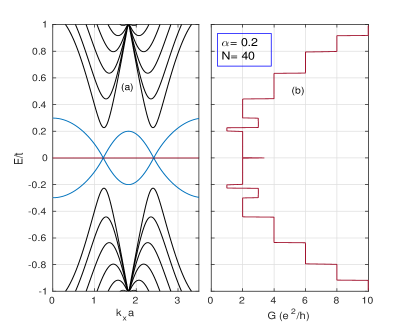
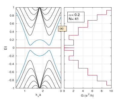
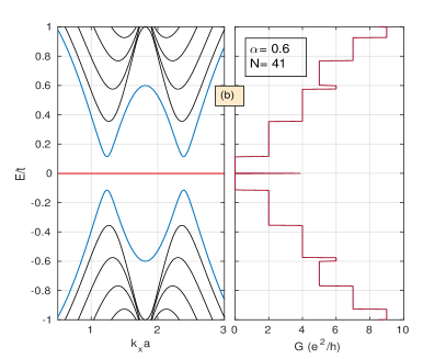
In this section, we present all transport coefficients numerically. First, we evaluate the conductance by using Eq. (24) and plot it with respect to the energy dispersion for in Fig. (8)a. Here, we keep the width with being the positive integer, in order to capture the gapless chiral edge modes. The conductance appears to be quantized as (r being the positive integer) with the ‘’ factor attributes to the two valleys. The integer ‘r’ accounts the number of transverse modes (black line) including the edge modes. With the increase of chemical potential, transverse modes start to penetrate through the chemical potential one by one, leading to the increase of conductance. Each transverse modes contributes conductance by units.

However, an unusual behavior is also seen in the region where edge modes (sky blue line) reside. Note that the pair of edge modes gives rise to the quantized conductance of unit before stepping down by one unit. This happen at a region where edge modes and 1st transverse modes interfere each other. A central peak in the conductance emerges corresponding to the dispersionless flat band. Similar peak resembles the divergence in dc bulk conductivity of such lattice under clean limit due to interband scatteringmate , at the band touching point between the flat band and the conic band. We find almost similar feature for , as shown in Fig. (9)b, except edge modes contribute for a wide range of energy.
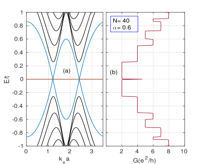
Now we explore how the conductance gets affected by changing for the gapped dispersion. To keep the band dispersion gapped, we take the width of the ribbon ( and ). The conductance is plotted against the gapped energy dispersion as a function of chemical potential in Fig. (9). It is already shown in Fig. (7) that the band gap increases slowly with the increase of . This fact has a direct impact on the conductance, as shown in Fig. (9), in terms of widening the zero conductance region with the increase of . This is a direct signature of the gap opening in transport measurement in a zigzag edge nanoribbon of such material provided the width has to be other than . Note that the degenerate flat bands also induce a central peak in the conductance spectra, however its height varies with the strength of . Another noticeable point here is that although the conductance steps down by unity in case of at , it disappears for . The origin of it can be attributed to the peculiar feature of the edge modes in the region in both cases.

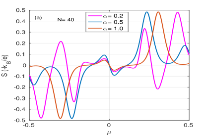
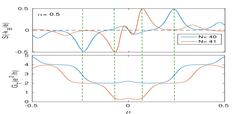
Now we plot thermopower by using Eq. (7) in Fig. (10). We consider both cases i.e., gapless and gapped dispersion by choosing the width and .
The thermopower for the width is plotted in Fig. (10)a which shows that non-zero has no much significant impact except the shifting of the thermopower peaks. However, a significant enhancement of thermopower can be found for gapped dispersion as can be seen in Fig. (10)b. It is worthwhile to mention that the thermopower can be further linked to the conductance via the standard Mott’s relation
| (26) |
which indicates that thermopower should be maximum around the slope of conductance spectrum, which can be confirmed from the plot Fig. (11). At the same time, the amplitude of thermopower decreases with as they are inversely related. On the other hand, it is noted from Fig. (10)b that thermopower increases with the strength of . Note that for gapped edge modes (), the thermopower is enhanced with the increase of , where as such enhancement does not occur with for gapless edge modes (). The reason can be attributed to how affects the product of the slope of conductance spectrum and it’s inverse. The enhancement of thermopower with the reveals that this product is much sensitive to the for gapped edge modes in comparison to the gapless edge modes.

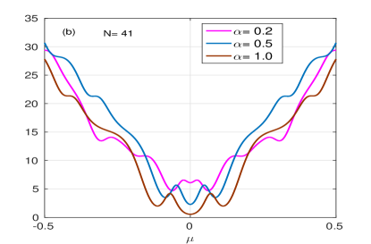
The corresponding thermal conductance are also evaluated by using Eq. (8) and plotted in Fig. (12). The Fig. (12) shows that unlike the case of thermopower, the thermal conductance is relatively much less sensitive to the variation of . The Fig. (8)a is plotted for the gapless edge modes i.e., . It shows that the effect of is relatively stronger for doped ribbon. On the other hand, for gapped system, effects of seems to be stronger around undoped situation.
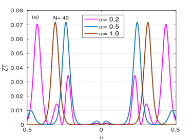
Finally, we look whether the dice lattice (or ) can of a way to improve the thermoelectric figure of merits of such hexagonal lattice. In order to address this concern, the thermoelectric figure of merit is plotted as a function of for two different widths in Fig. (13). It shows that the maximum value of the thermoelectric figure of merits remains unaltered with the variation of except a shift of the peaks for gapless edge modes (width ). However, on the other hand the figure of merits for is plotted in Fig. (13)a (gapped dispersion) which shows that figure of merits gets almost thirty times larger than than (13)b (gapless dispersion). We can conclude that the zigzag ribbon of a /dice lattice with gapped dispersion can be a better choice for thermoelectric material.
Line defects and its consequences:
The line defects in honeycomb lattice are formed or created out of the absence of one or more sublattices
in each unit celldefects1 ; defects2 . The presence of vacancy/line defects is one of the most common
issue which arises during experimental realization of such lattice. It has been previously
observed that such line defects yield some important consequences on the band structure
as well as in transport phenomena, such as opening the gap in graphenepeeters , valley polarizationwhite etc


In this section, we examine the effects of the line defects, formed out of the absence of sublattices in each unit cell at different distances from the edge. The effects of line defects/vacancy out of the absence of or sublattices were investigated previously in graphenepara ; peeters or silicenesilicene . In order to incorporate the line defect in tight-binding calculation, we set on-site energy to infinity at the missing site which prevents hoping between vacancy to nearest sites. The band dispersion of zigzag nanoribbon in presence of line defects are numerically presented in Fig. (14). The Fig. (14)a is plotted for line defects created out of the absence of atoms (C atoms) at where ‘’ is the sublattice number index with . It shows that the line defect causes drastic changes to the feature of the edge modes by enforcing them to touch at the middle of the two Dirac points. This feature can be expected to have significance consequences on the transport properties.
On other hand if the line defect is situated away from the zigzag edge i.e for distance , the effects on band spectrum appears to be almost negligible [see Fig. (14))b-(14)d].


In order to probe the consequences of the effects of line defects on transport properties, we also plot conductance in Fig. (15) for the line defect situated nearest to the edge i.e., . The most important signature of such line defect in the conductance is the appearance of conductance by instead of without line defects at low energy regime. The origin can be traced to the band dispersion in Fig. (14)a which exhibits extra Dirac-like point in addition to the two Dirac points, resulting three units of conductance. On the other hand, in absence of line defects, it is the two valleys which contribute two units of conductance in the low energy regime. A peculiar behavior occurs for where the conductance steps down and steps up by without defects. Such contradictory features in both cases can be attributed to the ways edge modes interfere with the transverse modes. We have also included the effects of line defects, formed out of the absence of A sublattices (A defects) close to the edge, on the conductance (shown in red line). It also exhibits quite distinct features in comparison to the C defects, in terms of the appearance of zero conductance on both side of the zero chemical potential. It suggests that A defects can induce a small gap in the band dispersion too. Subsequently, we also plot the thermopower in Fig. (15)b to reveal the effects of the nearest line defect. It is observed that although at low energy regime conductance gets affected by the presence of line defect, the thermopower seems to be lees sensitive to the C defects in terms of the amplitude. However, the A defects enhance the thermopower significantly.
As it is already shown in Fig. (14)b to (14)d that line defects, situated away from the edge has very less consequences and hence it can easily be anticipated that such defects would not have any significant impacts on electric or thermoelectric transport properties.
Finally we quickly comment here that the random disorder can be also treated in similar fashion by incorporating on-site potential, distributed randomly in the system. However, we have already noticed that the line defects can affect the feature of edge modes and corresponding transport signature only if it resides close to the edge. So we can conclude that the presence of random disorders can not have much significant impact unless it resides close to the edge.
V Summary and conclusions
In this work, we explore the roles of zigzag edge geometry of lattice on the band dispersion, conductance, thermopower and thermoelectric figure of merits under the continuous evolution of from graphene to dice lattice (by means of tuning ). We notice that the feature of edge modes are very much sensitive to the width of the nanoribbon. The energy dispersion can be gapped or gapless depending on the width of the ribbon. The edge modes are not dispersionless flat as found in graphene, rather it can be gapless chiral at the two valleys for specific width . Additionally, the slope of the gapless chiral edge modes increases with the increase of . On the other hand, the gap opening occurs between the pair of edge modes for the width of and the energy gap increases with the evolution towards dice lattice. Subsequently, we use tight-binding Green function approach to analyses the roles of edge modes and on electrical and thermoelectric transport coefficients of the zigzag nanoribbon based device, attached to the left and right lead. We found that possibility of reshaping the edge modes, by means of width and , can be exploited to improve the thermoelectric performances of such materials. It is found that the thermopower and thermoelectric figure of merits can be enhanced significantly by means of . The thermal conductance remains less sensitive to the in comparison to thermopower whereas the figure of merits exhibits a sharp enhancement. Finally, we have studied the consequences of line defects out of the absence of sublattices. We have found that such line defect has too weak impact on the band structure as well as on transport properties as long as the defects resides away from the edge. However, there is a drastic changes in the nature of the edge modes and corresponding transport signature if the line defects reside very near to the edge.
Acknowledgements.
The authors thank the Deanship of Scientific Research in King Faisal University (Saudi Arabia) for funding the facilities required for this research as part of the Research Grants Program Nasher: 186124)References
- (1) K. S. Novoselov, A. K. Geim, S. Morozov, D. Jiang, Y. Zhang, S. Dubonos, I. Grigorieva, and A. A. Firsov, Science 306, 666 (2004).
- (2) A. H. Castro Neto, F. Guinea, N. M. R. Peres, K. S. Novoselov, and A. K. Geim, Rev. Mod. Phys. 81, 109 (2009).
- (3) J. Vidal, R. Mosseri, and B. Doucot, Phys. Rev. Lett. 81, 5888 (1998).
- (4) J. D. Malcolm and E. J. Nicol, Phys. Rev. B 92, 035118 (2015).
- (5) Balazs Dora, Janik Kailasvuori, and R. Moessner, Phys. Rev. B 84, 195422 (2011).
- (6) Z. Lan, N. Goldman, A. Bermudez, W. Lu, and P. Ohberg, Phys. Rev. B 84, 165115 (2011).
- (7) A. Raoux, M. Morigi, J.-N. Fuchs, F. Pi ̵́echon, and G. Montambaux, Phys. Rev. Lett. 112, 026402 (2014).
- (8) D. Xiao, M. Chang, and Q. Niu, Rev. Mod. Phys. 82, 1959 (2010).
- (9) E. Illes, J. P. Carbotte, and E. J. Nicol, Phys. Rev. B 92, 245410 (2015).
- (10) Tutul Biswas and T. K. Ghosh, J. Phys.: Condens. Matter 28, 495302 (2016).
- (11) SK F. Islam and P. Dutta, Phys. Rev. B 96, 045418 (2017).
- (12) F. U. Daniel, D. Bercioux, M. Wimmer and W. Hausler, Phys. Rev. B 84, 115136 (2011).
- (13) E. Elles and E. J. Nicol, Phys. Rev. B 95, 235432 (2017)
- (14) E. Illes, and E. J. Nicol, Phys. Rev. B 94, 125435 (2016).
- (15) A. D. Kovacs, G. D. B. Dora, and J. Cserti, Phys. Rev. B 95, 035414 (2017).
- (16) J. D. Malcolm and E. J. Nicol, Phys. Rev. B 93, 165433 (2016).
- (17) Y. R. Chen et al., Phys. Rev. B 99, 045420 (2019).
- (18) B. Dey and T. K. Ghosh, Phys. Rev. B 98, 075422 (2018).
- (19) B. Dora, I. F. Herbut, and R. Moessner, Phys. Rev. B 90, 045310 (2014)
- (20) T. Biswas and T. K. Ghosh, J. phys.: Condens. Matter 30, 075301 (2018).
- (21) Nolas G S, Sharp J and Goldsmid H J, 2001 Thermoelectrics (Berlin: Springer)
- (22) F. J. DiSalvo, Science 285 703 (1999).
- (23) G. J. Snyder and E. S. Toberer, Nature Mater. 7 105 (2008).
- (24) E. H. Hwang, E. Rossi and S. D. Sarma, Phys. Rev. B 80, 235415 (2009).
- (25) S.-G. Nam, D. K. Ki, and H. J. Lee, Phys. Rev. B 82, 245416 (2010).
- (26) L. Hao and T. K. Lee, Phys. Rev. B 81, 165445 (2010).
- (27) Yuri M. Zuev, W. Chang and P. Kim, Phys. Rev. Lett. 102, 096807 (2009).
- (28) P. Wei, W. Bao, Y. Pu, C. N. Lau, and J. Shi, Phys. Rev. Lett. 102 166808 (2009).
- (29) M. S. Hossain, F. A. Dirini, F. Hossain and E. Skifidas, Sci. Rep. 5 11297 (2015).
- (30) V.-T. Tran et al., Sci. Rep. 7, 2313 (2017)
- (31) R. Ma, H. Geng, W. Y. Deng, M. N. Chen, L. Sheng, and D. Y. Xing, Phys. Rev. B 94, 125410 (2016).
- (32) E. Flores, J. R. Ares, A. Castellanos-Gomez, M. Barawi, I. J. Ferrer, and C. Sánchez, Appl. Phys. Lett. 106, 022102 (2015).
- (33) S. Lakshmi, S. Roche, and G. Cuniberti, Phys. Rev. B 80, 193404 (2009).
- (34) D. O. Oriekhov, E. V. Gorbar, and V. P. Gusynin, Low Temp. Phys. 44 1313 (2018).
- (35) L. Onsager, Phys. Rev. 37, 405 (1931)
- (36) L. Onsager, Phys. Rev. 38, 2265 (1931)
- (37) S. Datta, Electronic Transport in Mesoscopic Systems (Cambridge University Press, Cambridge, England, 1995).
- (38) S. H. Lv and Y. X. Li, J. Appl. Phys. 112, 053701 (2012).
- (39) C. W. Groth, M. Wimmer, A. R. Akhmerov, and X. Waintal, New J. Phys. 16, 063065 (2014).
- (40) P. Dutta, A. Saha and A. M. Jayannavar, Phys. Re. B 96, 115404 (2017).
- (41) J. Ferrer et. al., New J. Phys. 16, 093029 (2014).
- (42) H. Sadeghi, S. Sangtarash and Colin J. Lambert, Beilstein J. Nanotechnol. 6, 1176 (2015).
- (43) M. L. Sancho et al., J. Phys. F 14, 1205 (1984).
- (44) P. Dutta, S. K. Maiti, and S. Karmakar, J. Appl. Phys. 114, 034306 (2013).
- (45) Kh. Shakouri, H. Simchi, M. Esmaeilzadeh, H. Mazidabadi, and F. M. Peeters, Phys. Rev. B 92, 035413 (2015).
- (46) F. Khoeini, Kh. Shakouri, and F. M. Peeters, Phys. Rev. B 94, 125412 (2016).
- (47) M. Ezawa, New J. Phys. 16, 115004 (2014).
- (48) L. Yang et al., Phys. Rev. Lett 99, 186801 (2007).
- (49) V. Valeria et al., Phys. Rev. B 87, 115117 (2013).
- (50) Mate Vigh et al., Phys. Rev. B 88 161413 (R) (2013).
- (51) Y. Kobayashi, K.-I. Fukui, T. Enoki, and K. Kusakabe, Phys. Rev. 73, 125415 (2006).
- (52) Y. Niimi, T. Matsui, H. Kambara, K. Tagami, M. Tsukada, and H. Fukuyama, Phys. Rev. B 73, 085421 (2006).
- (53) R. N. Costa Filho, G. A. Farias, and F. M. Peeters, Phys. Rev. B 76, 193409 (2007)
- (54) D. Gunlycke and C. T. White, Phys. Rev. Lett. 106, 136806 (2011)