Plasmonics in Atomically-Thin Crystalline Silver Films
Abstract
Light-matter interaction at the atomic scale rules fundamental phenomena such as photoemission and lasing, while enabling basic everyday technologies, including photovoltaics and optical communications. In this context, plasmons –the collective electron oscillations in conducting materials– are important because they allow manipulating optical fields at the nanoscale. The advent of graphene and other two-dimensional crystals has pushed plasmons down to genuinely atomic dimensions, displaying appealing properties such as a large electrical tunability. However, plasmons in these materials are either too broad or lying at low frequencies, well below the technologically relevant near-infrared regime. Here we demonstrate sharp near-infrared plasmons in lithographically-patterned wafer-scale atomically-thin silver crystalline films. Our measured optical spectra reveal narrow plasmons (quality factor ), further supported by a low sheet resistance comparable to bulk metal in few-atomic-layer silver films down to seven Ag(111) monolayers. Good crystal quality and plasmon narrowness are obtained despite the addition of a thin passivating dielectric, which renders our samples resilient to ambient conditions. The observation of spectrally sharp and strongly confined plasmons in atomically thin silver holds great potential for electro-optical modulation and optical sensing applications.
I INTRODUCTION
The control of light at the nanoscale is a research frontier with applications in areas as diverse as biosensing Anker et al. (2008); Rodrigo et al. (2015), optoelectronics Mak and Shan (2016), nonlinear optics Danckwerts and Novotny (2007); Smirnova and Kivshar (2016), quantum optics Chang et al. (2006); Fakonas et al. (2014), and nanorobotics Zhou et al. (2015). Metallic nanostructures play a pivotal role in this context because they host collective electron oscillations, known as plasmons, which can interact strongly with light. This enables a large confinement of optical energy down to nanometer-sized regions, thereby enhancing the associated electromagnetic fields by several orders of magnitude relative to externally incident fields Li et al. (2003). Such appealing properties and the pursue of the noted applications have fueled intense research work into plasmonics to better understand and control these collective electronic excitations and cover a broad spectral range from the ultraviolet to the terahertz regimes. Progress has mainly relied on advances in nanofabrication and colloid chemistry, which allow producing engineered metallic nanostructures with on-demand plasmonic response Nagpal et al. (2009); Fan et al. (2010).
Plasmons in atomic-scale systems have emerged as a source of extraordinary properties resulting from the fact that they are sustained by a comparatively small number of charge carriers. Electron energy-loss spectroscopy has been instrumental in revealing plasmons in systems such as C60 molecules Keller and Coplan (1992), carbon and boron-nitride single-wall nanotubes Stéphan et al. (2002); Arenal et al. (2005), atomic gold wires grown on vicinal silicon surfaces Nagao et al. (2006), few-atomic-layer silver films Moresco et al. (1999), monolayer DySi2 Rugeramigabo et al. (2008), ultrathin indium Chung et al. (2010) and silicide Rugeramigabo et al. (2010) wires, and graphene Zhou et al. (2012). Additionally, ultrathin TiN films have been demonstrated for refractory plasmonics Guler et al. (2014); Shah et al. (2017), which contribute to configure the emerging field of transdimentional photonics Boltasseva and Shalaev (2019). Among these materials, high-quality graphene has been found to sustain low-energy plasmons when it is highly doped, exhibiting large electro-optical tunability Fei et al. (2012); Chen et al. (2012), long lifetime Ni et al. (2018), and strong confinement compared with conventional plasmonic metals Basov et al. (2016); Alcaraz Iranzo et al. (2018). Topological insulators Di Pietro et al. (2013) and black phosphorous Huber et al. (2017) have also been shown to display two-dimensional (2D) plasmons. Unfortunately, unlike noble-metal structures, the plasmons reported in these systems are either rather broad or lying at mid-infrared or lower frequencies, far from the technologically appealing near-infrared (NIR) regime. As a potential solution to this problem, electrochemically tunable plasmons have been revealed through optical spectroscopy in small polycyclic aromatic hydrocarbons Manjavacas et al. (2013); Lauchner et al. (2015), although their integration in fast commutation devices remains a challenge.
Atomically thin noble-metal films appear as a viable solution to achieve large electro-optical tunability Manjavacas and García de Abajo (2014); Yu et al. (2016) within the NIR spectral range. However, crystalline quality is required to lower optical losses to the promised level for these materials in the plasmonic spectral region. Indeed, the presence of multiple facets in few-nanometer nanoparticles Kreibig and Vollmer (1995); Scholl et al. (2012) and sputtered films Maniyara et al. (2019) produce broad plasmons characterized by a quality factor ( ratio of peak frequency to spectral width) of the order of , which averts their use in cutting-edge plasmonic applications.
Here, we report on the fabrication and the excellent plasmonic and electrical properties of wafer-scale atomically-thin crystalline silver films composed of only a few atomic layers. We use advanced surface-science techniques to fabricate and characterize Ag(111) films consisting of 7-20 atomic monolayers (MLs) on a clean Si(111) substrate, which we then cover with nm of Si in order to passivate them from air. The high atomic quality of the samples, which we confirm through scanning tunneling microscopy (STM), angle-resolved photoelectron spectroscopy (ARPES), high-resolution transmission electron microscopy (HRTEM), and low-energy electron diffraction (LEED), allows us to resolve sharp electronic vertical quantum-well states (QWs) and measure very low sheet resistances for thin films down to 7 ML Ag(111) (nm thick, sq, just a factor of 2 higher than the bulk estimate). We obtain spectral evidence of confined plasmons by using electron-beam (e-beam) nanolithography to pattern ribbons on the silver films, resulting in measured plasmons with quality factors nearing for 10 ML ( nm) films. These results reveal the ability of laterally-patterned few-atomic-layer atomically-flat silver to confine plasmons with similar lifetimes as bulk silver, thus extending 2D plasmonics into the technologically appealing NIR regime.
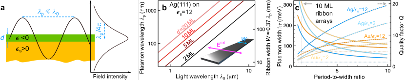
Like in graphene García de Abajo (2014), metal films of small thickness in the few atomic-layer range allow us to dramatically reduce the in-plane surface-plasmon wavelength . In the Drude model (see Methods), we find to scale linearly with and quadratically with the light wavelength as
| (1) |
(see Fig. 1b), where is a characteristic length that depends on the combination of metal and substrate materials (e.g., nm for Ag on Si). The confinement in the vertical direction is characterized by a symmetric exponential decay of the associated electric field intensity away from the film, extending a distance regardless of the choice of materials and metal thickness (Fig. 1a). The comparatively small number of electrons that support the plasmons in atomically-thin films makes them more susceptible to the environment, so that electrical gating with attainable carrier densities can produce significant plasmon shifts in single-atom-layer noble metals Manjavacas and García de Abajo (2014), while the addition and electrical gating of a graphene film results in dramatic modulation for thicker films up to a few nanometers Yu et al. (2016). Likewise, the presence of an analyte can shift the plasmon resonance and introduce molecule spectral fingerprints enhanced by the near field of the plasmons, similar to what has been observed with graphene Rodrigo et al. (2015). However, besides such plasmon shifts, all of these applications require spectrally narrow plasmons, so that spectral modulation results in strong changes in light transmission or scattering, and this in turn demands the fabrication of high-quality films.
II RESULTS AND DISCUSSION
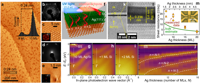
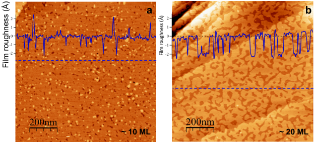
We epitaxially grow high-quality crystalline Ag(111) films on a Si(111)-oriented wafer substrate Neuhold and Horn (1997) with a controlled number of atomic monolayers under ultrahigh vacuum (UHV) conditions (see Methods). Through fine tuning of the growth parameters, we achieve films consisting of a single crystal domain on a cm2 chip scale, as revealed by STM with atomic resolution (see Figs. 2a and 6). The original reconstruction of atomically flat Si (Fig. 2c, where the upper and lower halves are empty and filled state images acquired with bias voltages of +2 V and -2 V, respectively) is removed upon Ag deposition, leaving an atomically flat Ag surface (Fig. 2e) that preserves crystal lattice orientation (cf. Figs. 2b and 2d). We approach the targeted number of Ag(111) monolayers (10 ML in Fig. 2a) with just a % fraction of regions differing by 1 ML thickness. We complete structural characterization by imaging a cross section of the film using HRTEM, which reveals a preservation of defect-free ordering of atomic Ag(111) monolayers (Fig. 2k,l) on the Si crystal substrate.
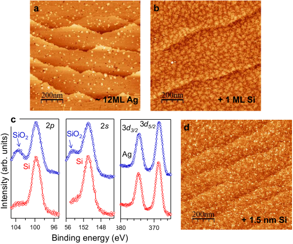
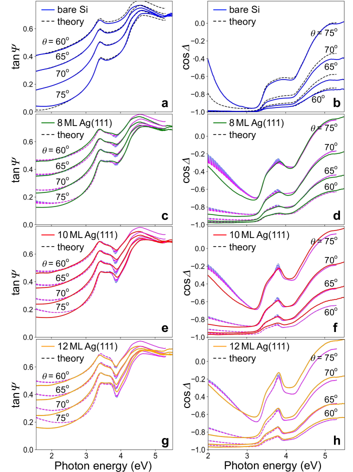
As plasmons are sustained by conduction electrons, we study the electronic band structure of the films, the small thickness of which produces discretization into a characteristic set of standing waves, encompassing vertical QWs Chiang (2000); Speer et al. (2006); Schiller et al. (2014) (labeled by in the sketch of Fig. 2f) and a surface-bound state (SS). Each of these QWs defines a band with nearly-free parabolic dispersion (effective mass ), as revealed by ARPES (Fig. 2g), which also show narrow lineshapes. We passivate our films with Si ( ML nominal thickness) in order to protect them during handling and patterning using e-beam nanolithography (see below). We note that high-quality unpassivated Ag(111) films are stable during hours when brought from UHV to ambient conditions without patterning Bao et al. (1993); Sanders et al. (2014); however, strain in the Ag/Si interface eventually leads to film dewetting (within days), initiated by pinholes Sanders et al. (2014) and leading to silver oxides and formation of rough films. This protective Si layer is rapidly oxidized upon exposure to air, while the underlying Ag film is unaffected for weeks (see Fig. 5). We remark that the addition of the thin Si capping layer causes the SS to disappear but does not affect the QW states (Fig. 2h,i). Control over thickness and high-quality of the films further allows us to experimentally observe a scaling of the QW binding energies with increasing film thickness (Fig. 2j), typical of a 1D particle-in-a-box system. We resolve QWs in all samples used in the present study, yielding an unambiguous determination of the number of layers in each Ag film. The presence and quality of the Ag film in the samples is further corroborated by ellipsometry measurements compared with bare Si substrates (see Fig. 8).
It is widely acknowledged fact that ultrathin metal films must experience strong surface scattering, and therefore see their electrical resistance sharply increased, as previous studies have indicated Namba (1970); Luo et al. (1994); Brandt et al. (2008); Hövel et al. (2010); Daghero et al. (2012). In contrast, the high crystal quality of our films produces very low levels of the sheet resistance (Fig. 2m), as revealed by four-probe measurements (see Fig. 7). In particular, we find the resistance to be only a factor of higher than the estimate based on the bulk resistivity of silver for films as thin as 7 ML Ag(111) (nm thickness). Because the film quality does not open new channels for inelastic collisions compared with the bulk, we thus attribute this factor of 2 to defects introduced by the capping Si layer, which has reduced crystallinity (see top of Fig. 2l), although some film damage during device fabrication cannot be ruled out. We attribute the large reduction of resistance in our films compared with previous studies, where films had a polycrystalline morphology, to the high crystallinity and absence of grain boundaries obtained by our followed epitaxial procedure (see Methods). The present results thus establish a much lower bound for the role played by surface scattering in the electrical resistance of high-quality crystalline silver films.
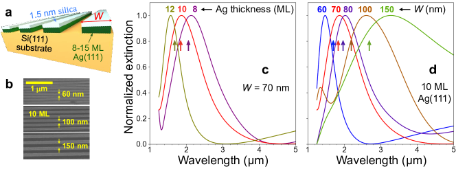
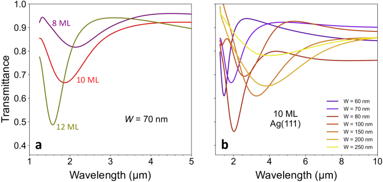
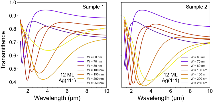
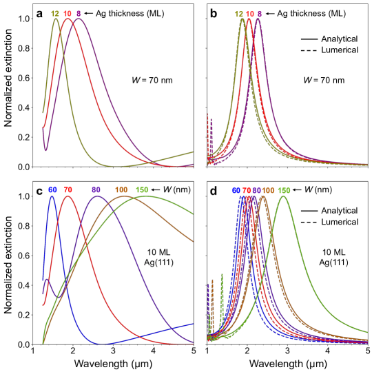
Plasmons in atomically-thin films are confined excitations with lateral wave vector greatly exceeding the light wave vector , which prevents direct light-plasmon coupling. An additional source of lateral momentum is needed to break this optical momentum mismatch, such as that provided by a pattern in the films. In this work, we use e-beam nanolithography (see Methods) to carve ribbons with the desired range of widths 50-500 nm, which allow us to explore plasmon wavelengths (Fig. 1b and Methods). The structure under consideration is sketched in Fig. 3a, while scanning electron microscopy (SEM) images of some of the actual structures are shown in Fig. 3b. The resulting measured optical spectra for different film thicknesses and ribbon widths are presented in Fig. 3c,d, where plasmon redshifts are clearly observed when reducing the thickness or increasing the width, in qualitative agreement with the analytical formula
| (2) |
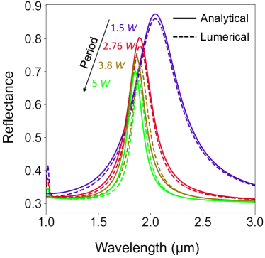
(vertical arrows in Fig. 3c,d), which predicts the light wavelength associated with the plasmon to scale linearly with the square root of the width-to-thickness aspect ratio . This expression, which follows from the Drude model combined with the relation between and (see Methods) Bondarev and Shalaev (2017), is in excellent agreement with a quantum-mechanical description of few-layer Ag films based upon the random-phase approximation combined with a realistic description of QWs in the films (see Fig. 14). Analytically calculated spectra (see Methods) have a similar level of agreement with measurements and nearly coincide with full electromagnetic simulations (see Fig.s 12 and 13). Additionally, the spectra of Fig. 3c,d reveal an increase in plasmon broadening with increasing ribbon width (see below).
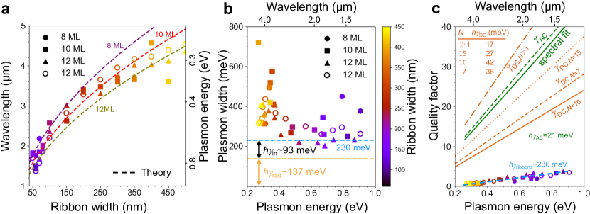
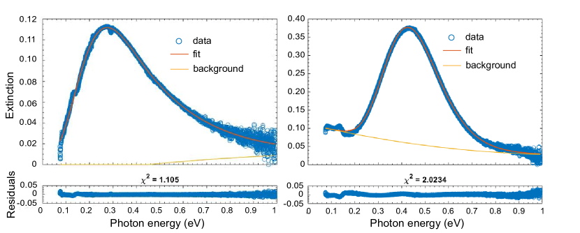
These plasmon characteristics are consistently corroborated upon inspection of different samples (see Figs. 9 and 10), the wavelengths and spectral widths of which are summarized in Fig. 4. In particular, when plotting the observed plasmon wavelength as a function of ribbon width, we obtain a good agreement with Eq. (2), despite deviations in individual structures, which we attribute to a variability in the actual width of the patterned ribbons. Additionally, we find a roughly constant plasmon width meV, which gives rise to a linear increase in with plasmon energy (see Fig. 4b,c and quality-factor extraction procedure in Fig. 11). In our experiments, we find values of approaching 4 at plasmon energies near 1 eV. These spectrally narrow plasmons are made possible by the small thickness of our metal films combined with their crystalline quality. Indeed, polycrystalline films in the few nanometer range hardly reach Maniyara et al. (2019). Additionally, spatially confined NIR plasmons in noble metals require the use of high aspect ratios ; before the present study, high-quality structures could only be obtained for much thicker films, therefore involving larger , and in consequence producing substantially broader plasmons due to coupling to radiation. Likewise, NIR plasmons in metallic colloids demand large particle aspect ratios, for which the observed quality factors are significantly smaller than 4 due to radiative losses as well Yu et al. (2017a), while in contrast to our films, the strategy of bringing the particle size to the few-nanometer range introduces additional plasmon quenching originating in finite-size effects Scholl et al. (2012) and thereby limiting the achievable .
The plasmon quality factors in our ribbon arrays are partially limited by radiative losses (see Fig. 1c). Indeed, as shown in Methods, the total plasmon damping rate is the sum of an intrinsic component and a geometry-dependent radiative component , where meV/nm for Ag(111) films on silicon. For our experiments we fabricate ribbons with a period-to-width ratio , which yields meV for 10 ML films. This value is shown in Fig. 4b as a lower dashed line; so we are left with an intrinsic damping meV, which is still over 4 times larger than the bulk value of meV derived from the measured permittivity of bulk silver Johnson and Christy (1972). We note that radiative losses should be negligible for arrays of large period-to-width ratio, thus suggesting a direct way to improve the quality factor with the same film quality (see Fig. 12).
The excess of intrinsic damping is presumably originating in sample damage incurred during the etching processes used for e-beam nanolithography (see Methods). Now, the question arises, how high can be for confined plasmons based upon high-quality metal films consisting of a few atomic layers (e.g., nm for 8 ML Ag(111))? We address this question by comparing our measured ’s with different estimates based upon the Drude expression neglecting radiative losses (Fig. 4c). Assuming the value meV obtained by fitting the measured Ag permittivity Johnson and Christy (1972) to a Drude tail in the sub-1 eV spectral region, we find (an order of magnitude larger than those observed here), in agreement with predictions based on the estimate of given by McPeak et al. (2015). This is also in good agreement with both the quality factors of spectra calculated in the long-wavelength limit (spectral fit) and the estimate obtained form the measured bulk DC conductivity (meV). We note that the sheet resistance measured from our films (Fig. 2m) leads according to the Drude model to predicted values for 10 ML Ag(111) films (see Methods) in the absence of radiative losses.
III CONCLUDING REMARKS
In brief, we report well-defined plasmons in atomically flat Ag(111) films grown on Si(111), with thickness as low as 8 ML (nm). The measured quality factors reach values . Further improvement of these results should include the exploration of thinner films down to 1-3 ML, which are however challenging because of the strain associated with the Ag/Si(111) interface. Following a two-step process (i.e., deposition at low temperature K followed by annealing to 300 K), we find the lowest thickness needed to produce atomically flat films using this procedure to be 6 ML. Nevertheless, 2ML Ag(111) films have been recently reported by employing a Ga/Si buffer layer He et al. (2014), showing rather flat surfaces and well-defined quantum-well states Starfelt et al. (2018). In our films, the crystalline quality of the fabricated Ag(111) films, which exhibit a clean electronic band structure consisting of quantized QWs, combined with the crystalline quality of the substrate, permit ruling out inelastic electron- and plasmon-scattering due to imperfections. However, the non-crystalline protecting capping layer can introduce inelastic coupling channels. Additionally, the etching processes used during e-beam lithography can cause sample damage, to which we attribute the reduction by half in film electrical conductance and by a factor of 5 in optical quality factor with respect to the maximum estimate in the studied spectral range, while another factor of in quality factor can be gained by reducing radiative losses (e.g., by increasing the period-to-width ratio of the ribbon arrays). Further improvement in nanofabrication could therefore increase the achieved plasmon quality factors. Nevertheless, the plasmons here observed should be already sufficiently narrow to produce large electro-optical modulation in the NIR Yu et al. (2016), while their reduced vertical and lateral size (down to nm and nm at 0.8 eV, see Figs. 1a and 4a) are ideally suited for enhancing the interaction with neighboring molecules, thus holding great potential for optical sensing.
METHODS
Fabrication of Atomically-Thin Silver Films. Our Ag/Si(111) samples were prepared inside an UHV chamber at mbar base pressure. We used mm2 n-doped Si(111) chips with specific resistance 120-340 cm as bare substrates. The dopant concentration of Si (1.3- cm-3) was chosen to guarantee the electrical conduction required by surface science techniques, while not influencing the plasmonic performance of the silver films. Once inside the UHV chamber, the Si(111) chips were degassed overnight at 900 K and subsequently flashed to 1400 K for 20-30 sec to remove the native silicon oxide. The sample temperature was slowly reduced to 600 K, maintained at this temperature for 30 min, and then cooled down to room temperature. This resulted in the formation of a defect-free, atomically clean Si(111) surface with a 77 reconstruction. Silver atoms were sublimated from an electron-bombardment evaporator, which was calibrated to sub-monolayer accuracy using a quartz microbalance monitor in combination with probing the distinct 1-2 ML Ag/Cu(111) surface states by photoemission Schiller et al. (2005). Silver films were grown on Si(111) following this two-step process. The Si(111) substrate was kept at 100-120 K during Ag deposition and slowly annealed to room temperature afterwards Miyazaki and Hirayama (2008). The deposition rate was ML/min, although a similar film quality was obtained within the 0.1-0.5 ML/min range; the crucial parameter here is the deposition temperature, which was required to be K.
Surface-Science Characterization. The atomic and electronic structure of the Si substrate and the grown Ag films were characterized by LEED, STM, and ARPES. STM data were collected using an Omicron VT setup operating at room temperature. ARPES measurements were performed using a SPECS Phoibos 150 electron analyzer equipped with a monochromatized He gas discharge lamp operating at the He I excitation energy (21.2 eV), with an electron energy and angular resolution of 30 meV and , respectively. The diameter of the UV light beam was mm at the sample surface. Sample transfer between STM and ARPES setups was made without breaking UHV conditions. Prior to atmosphere exposure, the samples were capped by a Si protection layer (nm nominal thickness), evaporated by direct heating of a Si chip with the same doping level as the substrate. The robustness and aging of the films was monitored by X-ray photoemission spectroscopy (XPS, see Fig. 5).
HRTEM Characterization. Electron-transparent (nm thickness) cross-sectional lamellas of the samples were prepared by first sputtering a platinum layer for protection, followed by carving using a FEI Helios NanoLab 600 dual beam SEM/focused-ion-beam (FIB) system. After transfer of the lamellas to a copper grid, they were imaged using a JEOL JEM-2100 HRTEM operated at 200 kV.
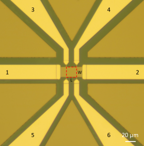
Sheet Resistance Measurements. Ultrathin silver films were etched into a Hall-bar structure by argon plasma using an Oxford Plasmalab 100 reaction-ion etching (RIE) system. A Poly (methyl methacrylate) (PMMA) layer was used as the etch mask. Contact electrodes were formed by depositing a Cr/Au/Al (3/60/190 nm) layer followed by lift-off. All structures were patterned by a Raith EBPG 5000+ e-beam lithography system. A four-probe scheme Smits (1958) (Fig. 7) was used to extract the sheet resistance. The electrical characterization was performed in a Lakeshore probe station operating at mbar. An Agilent B1500A semiconductor parameter analyzer was used for all electrical measurements.
Electron-Beam Nanolithography. Passivated silver-film chips were uniformly spin-coated with nm ZEP520A resist for 1 min at 6000 rpm. Ribbons were then written using a RAITH150-Two e-beam lithography system, followed by development in amyl acetate and reactive-ion etching for min with an Ar and CHF3 mixture in a RIE Oxford Plasmalab 80 Plus system. Periodic arrays of 50-1000 nm-wide ribbons were fabricated with a footpring of m2 per sample and period-to-width ratio. Importantly, although standard procedures usually involve baking at 150-180∘C after spin-coating to induced a phase transition to glass in the resist, we skipped this step to avoid Ag film damage, at the expense of having a more fragile resist that required careful calibration of the RIE gas mixture and etching time to preserve the etching mask.
Optical Characterization. We used a SOPRA GES-5E system to perform ellipsometry (Fig. 8) for incidence angles in the 60-75∘ range over the UV-NIR photon energy region (1.5-5 eV). Optical transmission/reflectance spectra (Figs. 9 and 10) were collected using a BRUKER HYPERION fourier-transform infrared (FTIR) spectrometer operating in the 1.3-m range.
Analytical Simulations. The plasmon dispersion relation (parallel wave vector as a function of frequency ) of a homogeneous thin film is given in the quasistatic limit by García de Abajo (2014)
where and are the permittivities of the media on either side of the film, while is the 2D conductivity. Assuming local response, we write the latter as
which is proportional to the film thickness , and where stands for the metal permittivity; this is an excellent approximation for the materials and film thicknesses under consideration even when compared with quantum-mechanical simulations (see Fig. 14). Adopting the Drude model Ashcroft and Mermin (1976), we approximate in terms of the bulk plasma frequency and the intrinsic damping rate (assuming ), which leads to the dispersion relation , and this in turn allows us to write the in-plane plasmon wavelength defined by as (i.e., Eq. (1) in the main text), where
and is the free-space light wavelength. For Ag films (eV Johnson and Christy (1972)) deposited on silicon () and coated with ZEP502A resist (), we find nm, which renders at light wavelengths below m when spans a few atomic layers (below ML), thereby justifying our using the quasistatic limit, although retardation effects can become apparent for longer wavelengths and thicker films. Incidentally, the resist is not removed from the samples before plasmon measurements, but the penetration depth is smaller than the resist thickness (100 nm), thus justifying the use of the resist permittivity in the above expression for .
We remark that the above results assume a small film thickness compared with the plasmon wavelength , while the reduction of the metal film response to a surface conductivity is valid if is also small compared with the skin depth nm in Ag. Additionally, in the quasistatic limit, the electric field is longitudinal () and divergenceless (), therefore displaying a symmetric pattern relative to the negligibly-thick film (we refer to a recent study Dias and García de Abajo (2019) for more details). In particular, the electric field associated with the plasmon has symmetric (antisymmetric) in-plane (out-of-plane) components with respect to the normal coordinate and admits the expression Dias and García de Abajo (2019) for propagation along the in-plane direction , from which an exponential decay away from the film is predicted with a fall in intensity at a distance from the film (see Fig. 1a in the main text). We note that the field is however asymmetric if the film thickness is not small compared with both the plasmon wavelength and the metal skin depth. The above expression for the field also allows us to write the in-plane plasmon propagation distance (for decay in intensity) as . Using the dispersion relation noted above, we find , where (e.g., taking meV for Ag, as obtained from optical data Johnson and Christy (1972), we have m); the propagation distance is then (independent of metal thickness) times the plasmon wavelength (proportional to metal thickness). Incidentally, a plasmon lifetime is directly inherited from the Drude model in the absence of radiative losses (a good approximation for ) and substrate absorption (Si losses are negligible in the studied spectral range within the plasmon penetration depth), leading to a plasmon quality factor (frequency-to-width ratio) . This relation is used in Fig. 4c of the main text with various estimates for (see below as wel). We also find useful to write the propagation distance as .
For ribbon arrays, plasmons are excited under transverse polarization (i.e., with the electric field oriented across the width of the ribbons, see Fig. 1b in the main text), whereas a featureless weak absorption is produced when the incident light field is parallel to the ribbons. Consequently, we concentrate on the former in what follows and adopt a previously reported model García de Abajo (2014) to calculate the normal-incidence transverse-polarization transmission coefficient as
| (3) |
where is the average refractive index of the media above (air, neglecting the resist layer in the coupling to radiation) and below (Si) the metal layer, is the ribbon polarizability per unit length, describes radiative coupling, is the lattice period, accounts for inter-ribbon interactions in the dipolar approximation, and is the average permittivity of the surrounding media. We express the polarizability
in terms of the 2D conductivity of the metal and only consider the dominant contribution of the dipolar plasmon resonance corresponding to parameters Yu et al. (2017b) and , which depend on the ribbon thickness-to-width aspect ratio . Finally, the 2D conductivity is related to the metal permittivity as , where we approximate the capping layer of thickness nm as an additional term in with . We use tabulated optical data for silver Johnson and Christy (1972) () and crystalline silicon Aspnes and Studna (1983) (). Reassuringly, the analytical theory just presented produces spectra in nearly full agreement with numerical electromagnetic simulations (see Figs. 12 and 13). Incidentally, this analysis of ribbon arrays ignores the resist, which our numerical simulations (not shown) predict to only cause minor plasmon redshifts.
The transverse dipolar plasmon of a single ribbon is signaled by a divergence in (i.e., ), which combined with the dispersion relation of the extended film leads to the condition
for . Adopting this expression and neglecting inter-ribbon interactions, we can use Eq. (1) to readily obtain Eq. (2) in the main text. It should be noted that inter-ribbon interaction can produce a small redshift correction in the plasmon position (see Fig. 12).
We find it convenient to arrange the above expressions above expressions by neglecting the capping layer and ap- proximating the silver permittivity as in order to express the transmission coefficient of the array (Eq. (3)) as
where
| (4) |
is the resulting plasmon resonance of the array under normal incidence, whereas
is the total plasmon damping rate, contributed by the intrinsic component and a radiative component
| (5) |
The first term inside the square root of Eq. (4) describes the plasmon frequency of the isolated ribbon, while the second term accounts for a redshift due to inter-ribbon interaction. We note that radiative damping (Eq. (5)) decreases with increasing array period , so sharper plasmons are expected in the limit of large separations, for which (see Fig. 1c); incidentally, we have neglected radiative contributions to the damping of individual ribbons under the assumption . When we specify Eq. (5) to Ag(111) ribbons on silicon, we find , where meV/nm.
Drude Damping Estimated from the Electrical Resistance. We use the expression
to convert DC resistivities from SI to CGS units. Then, we use the Drude model to write the damping rate as
Damping rates in Fig. 4c are obtained by applying these formulas to the SI resistivities for bulk silver () and for silver films consisiting of Ag(111) atomic layers (), where nm is the atomic layer spacing and is the average sheet resistance (for each value of ) obtained from the data points presented in Fig. 2m.
Acknowledgements.
We thank Marta Autore, Josep Canet-Ferrer, Rainer Hillenbrand, Johan Osmond, and Frederik Schiller for technical support and helpful discussions. V.M. and F.J.G.A. gratefully acknowledge generous help and hospitality from Luis Hueso and Ralph Gay at CIC nanoGUNE, where nanolithography and FTIR were performed. This work has been supported in part by ERC (Advanced Grant 789104-eNANO), the Spanish MINECO (MAT2017-88492-R, SEV2015-0522, and PCIN-2015-155, and MAT2016-78293-C6-6-R), the Catalan CERCA Program, the Basque Government (IT-1255-19), Fundació Privada Cellex, and the US National Science Foundation CAREER Award (1552461).ADDITIONAL FIGURES
References
- Anker et al. (2008) J. N. Anker, W. P. Hall, O. Lyandres, N. C. Shah, J. Zhao, and R. P. Van Duyne, Nat. Mater. 7, 442 (2008).
- Rodrigo et al. (2015) D. Rodrigo, O. Limaj, D. Janner, D. Etezadi, F. J. García de Abajo, V. Pruneri, and H. Altug, Science 349, 165 (2015).
- Mak and Shan (2016) K. F. Mak and J. Shan, Nat. Photon. 10, 216 (2016).
- Danckwerts and Novotny (2007) M. Danckwerts and L. Novotny, Phys. Rev. Lett. 98, 026104 (2007).
- Smirnova and Kivshar (2016) D. Smirnova and Y. S. Kivshar, Optica 3, 1241 (2016).
- Chang et al. (2006) D. E. Chang, A. S. Sörensen, P. R. Hemmer, and M. D. Lukin, Phys. Rev. Lett. 97, 053002 (2006).
- Fakonas et al. (2014) J. S. Fakonas, H. Lee, Y. A. Kelaita, and H. A. Atwater, Nat. Photon. 8, 317 (2014).
- Zhou et al. (2015) C. Zhou, X. Duan, and N. Liu, Nat. Commun. 6, 8102 (2015).
- Li et al. (2003) K. R. Li, M. I. Stockman, and D. J. Bergman, Phys. Rev. Lett. 91, 227402 (2003).
- Nagpal et al. (2009) P. Nagpal, N. C. Lindquist, S.-H. Oh, and D. J. Norris, Science 325, 594 (2009).
- Fan et al. (2010) J. A. Fan, C. H. Wu, K. Bao, J. M. Bao, R. Bardhan, N. J. Halas, V. N. Manoharan, P. Nordlander, G. Shvets, and F. Capasso, Science 328, 1135 (2010).
- Keller and Coplan (1992) J. W. Keller and M. A. Coplan, Chem. Phys. Lett. 193, 89 (1992).
- Stéphan et al. (2002) O. Stéphan, D. Taverna, M. Kociak, K. Suenaga, L. Henrard, and C. Colliex, Phys. Rev. B 66, 155422 (2002).
- Arenal et al. (2005) R. Arenal, O. Stéphan, M. Kociak, D. Taverna, A. Loiseau, and C. Colliex, Phys. Rev. Lett. 95, 127601 (2005).
- Nagao et al. (2006) T. Nagao, S. Yaginuma, T. Inaoka, and T. Sakurai, Phys. Rev. Lett. 97, 116802 (2006).
- Moresco et al. (1999) F. Moresco, M. Rocca, T. Hildebrandt, and M. Henzler, Phys. Rev. Lett. 83, 2238 (1999).
- Rugeramigabo et al. (2008) E. P. Rugeramigabo, T. Nagao, and H. Pfnür, Phys. Rev. B 78, 155402 (2008).
- Chung et al. (2010) H. V. Chung, C. J. Kubber, G. Han, S. Rigamonti, D. Sánchez-Portal, D. Enders, A. Pucci, and T. Nagao, Appl. Phys. Lett. 96, 243101 (2010).
- Rugeramigabo et al. (2010) E. P. Rugeramigabo, C. Tegenkamp, H. Pfnür, T. Inaoka, and T. Nagao, Phys. Rev. B 81, 165407 (2010).
- Zhou et al. (2012) W. Zhou, J. Lee, J. Nanda, S. T. Pantelides, S. J. Pennycook, and J. C. Idrobo, Nat. Nanotech. 7, 161 (2012).
- Guler et al. (2014) U. Guler, A. Boltasseva, and V. M. Shalaev, Science 344, 263 (2014).
- Shah et al. (2017) D. Shah, H. Reddy, N. Kinsey, V. M. Shalaev, and A. Boltasseva, Adv. Mater. 5, 2816 (2017).
- Boltasseva and Shalaev (2019) A. Boltasseva and V. M. Shalaev, ACS Photon. 6, 1 (2019).
- Fei et al. (2012) Z. Fei, A. S. Rodin, G. O. Andreev, W. Bao, A. S. McLeod, M. Wagner, L. M. Zhang, Z. Zhao, M. Thiemens, G. Dominguez, et al., Nature 487, 82 (2012).
- Chen et al. (2012) J. Chen, M. Badioli, P. Alonso-González, S. Thongrattanasiri, F. Huth, J. Osmond, M. Spasenović, A. Centeno, A. Pesquera, P. Godignon, et al., Nature 487, 77 (2012).
- Ni et al. (2018) G. X. Ni, A. S. McLeod, Z. Sun, L. Wang, L. Xiong, K. W. Post, S. S. Sunku, B.-Y. Jiang, J. Hone, C. R. Dean, et al., Nature 557, 530 (2018).
- Basov et al. (2016) D. N. Basov, M. M. Fogler, and F. J. García de Abajo, Science 354, aag1992 (2016).
- Alcaraz Iranzo et al. (2018) D. Alcaraz Iranzo, S. Nanot, E. J. C. Dias, I. Epstein, C. Peng, D. K. Efetov, M. B. Lundeberg, R. Parret, J. Osmond, J.-Y. Hong, et al., Science 360, 291 (2018).
- Di Pietro et al. (2013) P. Di Pietro, M. Ortolani, O. Limaj, A. Di Gaspare, V. Giliberti, F. Giorgianni, M. Brahlek, N. Bansal, N. Koirala, S. Oh, et al., Nat. Nanotech. 8, 556 (2013).
- Huber et al. (2017) M. A. Huber, F. Mooshammer, M. Plankl, L. Viti, F. Sandner, L. Z. Kastner, T. Frank, J. Fabian, M. S. Vitiello, T. L. Cocker, et al., Nat. Nanotech. 12, 207 (2017).
- Manjavacas et al. (2013) A. Manjavacas, F. Marchesin, S. Thongrattanasiri, P. Koval, P. Nordlander, D. Sánchez-Portal, and F. J. García de Abajo, ACS Nano 7, 3635 (2013).
- Lauchner et al. (2015) A. Lauchner, A. Schlather, A. Manjavacas, Y. Cui, M. J. McClain, G. J. Stec, F. J. García de Abajo, P. Nordlander, and N. J. Halas, Nano Lett. 15, 6208 (2015).
- Manjavacas and García de Abajo (2014) A. Manjavacas and F. J. García de Abajo, Nat. Commun. 5, 3548 (2014).
- Yu et al. (2016) R. Yu, V. Pruneri, and F. J. García de Abajo, Sci. Rep. 6, 32144 (2016).
- Kreibig and Vollmer (1995) U. Kreibig and M. Vollmer, Optical Properties of Metal Clusters (Springer-Verlag, Berlin, 1995).
- Scholl et al. (2012) J. A. Scholl, A. L. Koh, and J. A. Dionne, Nature 483, 421 (2012).
- Maniyara et al. (2019) R. A. Maniyara, D. Rodrigo, R. Yu, J. Canet-Ferrer, D. S. Ghosh, R. Yongsunthon, D. E. Baker, A. Rezikyan, F. J. García de Abajo, and V. Pruneri, Nat. Photon. 13, 328 (2019).
- García de Abajo (2014) F. J. García de Abajo, ACS Photon. 1, 135 (2014).
- Neuhold and Horn (1997) G. Neuhold and K. Horn, Phys. Rev. Lett. 78, 1327 (1997).
- Chiang (2000) T.-C. Chiang, Surf. Sci. Rep. 39, 181 (2000).
- Speer et al. (2006) N. J. Speer, S.-J. Tang, T. Miller, and T.-C. Chiang, Science 314, 804 (2006).
- Schiller et al. (2014) F. Schiller, Z. M. Abd El-Fattah, S. Schirone, J. Lobo-Checa, M. Urdanpilleta, M. Ruiz-Oses, J. Cordon, M. Corso, D. Sánchez-Portal, A. Mugarza, et al., New J. Phys. 16, 123025 (2014).
- Bao et al. (1993) X. Bao, J. V. Barth, G. Lehmpfuhl, R. Schuster, Y. Uchida, R.Schlögl, and G. Ertl, Surf. Sci. 284, 14 (1993).
- Sanders et al. (2014) C. E. Sanders, C. Zhang, G. L. Kellogg, and C.-K. Shih, Surf. Sci. 630, 168 (2014).
- Namba (1970) Y. Namba, Jpn. J. Appl. Phys. 9, 1326 (1970).
- Luo et al. (1994) E. Z. Luo, S. Heun, M. Kennedy, J. Wollschläger, and M. Henzler, Phys. Rev. B 49, 4858 (1994).
- Brandt et al. (2008) T. Brandt, M. Hövel, B. Gompf, and M. Dressel, Phys. Rev. B 78, 205409 (2008).
- Hövel et al. (2010) M. Hövel, B. Gompf, and M. Dressel, Phys. Rev. B 81, 035402 (2010).
- Daghero et al. (2012) D. Daghero, F. Paolucci, A. Sola, M. Tortello, G. A. Ummarino, M. Agosto, R. S. Gonnelli, J. R. Nair, and C. Gerbaldi, Phys. Rev. Lett. 108, 066807 (2012).
- Bondarev and Shalaev (2017) I. V. Bondarev and V. M. Shalaev, Opt. Mater. Express 7, 3731 (2017).
- Yu et al. (2017a) R. Yu, L. M. Liz-Marzán, and F. J. García de Abajo, Chem. Soc. Rev. 46, 6710 (2017a).
- Johnson and Christy (1972) P. B. Johnson and R. W. Christy, Phys. Rev. B 6, 4370 (1972).
- McPeak et al. (2015) K. M. McPeak, S. V. Jayanti, S. J. P. Kress, S. Meyer, A. R. Stelio Iotti, , and D. J. Norris, ACS Photon. 2, 326 (2015).
- He et al. (2014) J.-H. He, L.-Q. Jiang, J.-L. Qiu, L. Chen, and K.-H. Wu, Chin. Phys. Lett. 31, 128102 (2014).
- Starfelt et al. (2018) S. Starfelt, H. M. Zhang, and L. S. O. Johansson, Phys. Rev. B 97, 195430 (2018).
- Schiller et al. (2005) F. Schiller, J. Cordón, D. V. A. Rubio, and J. E. Ortega, Phys. Rev. Lett. 94, 016103 (2005).
- Miyazaki and Hirayama (2008) M. Miyazaki and H. Hirayama, Surf. Sci. 602, 276 (2008).
- Smits (1958) F. M. Smits, Bell System Tech. J. 37, 711 (1958).
- Ashcroft and Mermin (1976) N. W. Ashcroft and N. D. Mermin, Solid State Physics (Harcourt College Publishers, Philadelphia, 1976).
- Dias and García de Abajo (2019) E. J. C. Dias and F. J. García de Abajo, ACS Nano 13, 5184 (2019).
- Yu et al. (2017b) R. Yu, J. D. Cox, J. R. M. Saavedra, and F. J. García de Abajo, ACS Photon. 4, 3106 (2017b).
- Aspnes and Studna (1983) D. E. Aspnes and A. A. Studna, Phys. Rev. B 27, 985 (1983).
- (63) See Optical Data from Sopra SA at http://www.sspectra.com/sopra.html (accessed on February 28, 2019).
- Echarri et al. (2019) A. R. Echarri, J. D. Cox, and F. J. García de Abajo, Optica 6, 630 (2019).
- Chulkov et al. (1999) E. Chulkov, V. Silkin, and P. Echenique, Surf. Sci. 437, 330 (1999).