Quantum Effects in the Acoustic Plasmons of Atomically-Thin Heterostructures
Abstract
Recent advances in nanofabrication technology now enable unprecedented control over 2D heterostructures, in which single- or few-atom thick materials with synergetic opto-electronic properties can be combined to develop next-generation nanophotonic devices. Precise control of light can be achieved at the interface between 2D metal and dielectric layers, where surface plasmon polaritons strongly confine electromagnetic energy. Here we reveal quantum and finite-size effects in hybrid systems consisting of graphene and few-atomic-layer noble metals, based on a quantum description that captures the electronic band structure of these materials. These phenomena are found to play an important role in the metal screening of the plasmonic fields, determining the extent to which they propagate in the graphene layer. In particular, we find that a monoatomic metal layer is capable of pushing graphene plasmons toward the intraband transition region, rendering them acoustic, while the addition of more metal layers only produces minor changes in the dispersion but strongly affects the lifetime. We further find that a quantum approach is required to correctly account for the sizable Landau damping associated with single-particle excitations in the metal. We anticipate that these results will aid in the design of future platforms for extreme light-matter interaction on the nanoscale.
I Introduction
The isolation of monolayer graphene Novoselov et al. (2004) has stimulated extensive research efforts in two-dimensional (2D) materials, due in part to their unique electronic and optical properties, which are well-suited for use in compact, ultra-efficient photonic and opto-electronic devices Xia et al. (2014). Polaritons in 2D materials are particularly appealing in the field of nano-optics because they can confine external electromagnetic fields into extremely small volumes Alcaraz Iranzo et al. (2018), enabling control of quantum and nonlinear optical phenomena on the nanoscale Cox and García de Abajo (2014). Additionally, 2D polaritons are extremely sensitive to their surrounding environment, a property that renders them as good candidates for optical sensing Lee and El-Sayed (2006), but also as enablers of new electro-optical functionalities when different atomically-thin materials are combined to form heterostructures Geim and Grigorieva (2013); Basov et al. (2016).
Surface-plasmon polaritons (SPPs) are formed when light hybridizes with the collective oscillations of charge carriers at the interface between dielectric and conducting media Economou (1969), offering particularly strong confinement of electromagnetic energy down to truly nanometer length scales Barnes et al. (2003). Noble metals are the traditional material platform used in plasmonics research, although they are difficult to actively tune and suffer from large ohmic losses Mulvaney et al. (2006); Khurgin (2015). Graphene can help circumvent these limitations, as it supports highly-confined and long-lived plasmonic resonances that can be electrically modulated Fei et al. (2011); Chen et al. (2012); Fei et al. (2012). In particular, the encapsulation of exfoliated monolayer graphene (MG) in hexagonal boron nitride (hBN) has been shown to dramatically improve the quality factor of plasmon resonances, with measured lifetimes of propagating modes ps at room temperature Woessner et al. (2015), and even beyond 1 ps at lower temperatures Ni et al. (2018). However, graphene plasmon studies have been so far limited to the terahertz and mid-infrared (mid-IR) spectral domains because the resonance energies of these excitations are severely constrained by the doping densities that can be sustained by the carbon layer, although some prospects have been formulated to extend their range of operation into the near-IR region García de Abajo (2014).
Hybrid systems comprising noble metal layers and graphene potentially alleviate the limitations of plasmons in both of these materials by capitalizing on the appealing electrical tunability of graphene combined with the visible and near-IR plasmon resonances of noble metals. For example, tuning the damping of metal plasmons with electrostatically-gated graphene has been shown to enable a small degree of electrical tunability Emani et al. (2012), while this approach has been predicted to reach order-unity active modulation if a graphene layer is deposited on a thin metallic film Yu et al. (2016). Still in the mid-IR, the proximity of a metal film in a heterostructure comprising hBN-encapsulated graphene and optically-thick metal surfaces has been recently demonstrated to push plasmon confinement down to a few atomic lengths outside the graphene sheet by rendering the plasmon dispersion acoustic, running close to the continuum of graphene intraband excitations Lundeberg et al. (2017); Iranzo et al. (2018). Indeed, acoustic plasmons can result from the hybridization of modes in two neighboring metal surfaces Dionne et al. (2006), or also in graphene and a metal surface, emerging as a low-energy branch in the energy-momentum dispersion diagram Principi et al. (2011). In contrast to the intuition that metal screening quenches the graphene response, an acoustic plasmon branch has been predicted to manifest itself even when graphene is directly deposited on the metal without a spacer Principi et al. (2018). For atomic-scale graphene-metal separations, the nonlocal nature of the optical response in both the metal and graphene layers plays an important role, demanding a rigorous theoretical treatment to accurately describe the dispersion and lifetime of acoustic plasmons Dias et al. (2018). The hydrodynamic model Bloch (1933); Ritchie (1957); David and García de Abajo (2014); Mortensen et al. (2014) has been extensively employed in this context, consisting in describing thin metal films within the framework of classical electrodynamics and introducing conduction electrons as a classical plasma Raza et al. (2013a); Moreau et al. (2013); David et al. (2013); Ciraci et al. (2013); David and Christensen (2017). However, the hydrodynamical model neglects effects associated with the electronic band structure that can become important when optical confinement reaches the atomic length scale Jaklevic and Lambe (1975); Hövel et al. (2010); Qian et al. (2015); Raza et al. (2013b); Bondarev and Shalaev (2017). First principles simulations have also been employed based on time-dependent density-functional theory to characterize the plasmons of metal films Runge and Gross (1984); Pitarke et al. (2007); Yan et al. (2011); Laref et al. (2013); Schiller et al. (2014); Sundararaman et al. (2018); Shah et al. (2018), but they involve computationally expensive simulations that are difficult to extend to systems comprising heterostructures and lacking a single overall atomic periodicity. Nevertheless, a more rigorous study is still pending on the nonlocal effects that affect the plasmons supported by thin metal films and their hybridization with graphene modes.
Here, we explore the role played by quantum and finite-size effects in the acoustic plasmons resulting from hybridization of MG with few-atom-thick metallic films. We simulate the graphene and the metal within the random-phase approximation (RPA), incorporating in the metal phenomenological information on the main characteristics of the conduction electronic band structure, such as surface states, electron spill out, and a directional band gap associated with bulk atomic-layer corrugation. Comparison among different levels of approximation to the electron confinement potential, as well as to classical electromagnetic approaches, reveals that quantum and finite-size effects produce dramatic changes in the plasmon lifetime, which require a quantum description of the system to be properly accounted for. Remarkably, we find that a single metal monolayer can render the graphene plasmon dispersion acoustic, while the addition of more monolayers hardly modifies the dispersion but does change the lifetime. Also, the plasmon lifetime is strongly affected by Landau damping in the metal, which is automatically incorporated in the RPA description. Our study and methodology are of general use for the description of plasmons in thin metal films and their interaction with nearby 2D materials.
II Results and discussion
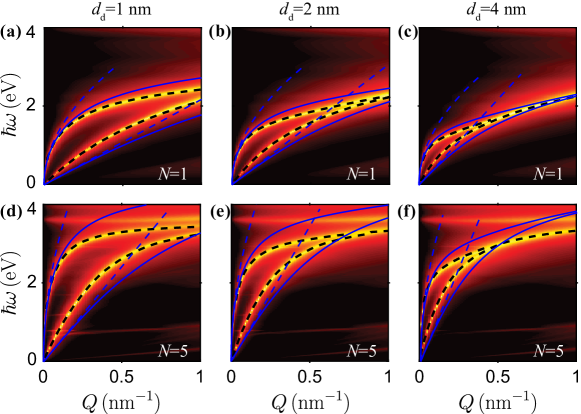
Acoustic plasmons result from the repulsion between modes in closely spaced metallic films Economou (1969) and their name derives from the linear relation between their frequency and in-plane wave vector , similar to acoustic waves. A tutorial description of this concept is provided by considering metal films of small thickness and local permittivity , the response of which can be approximated as that of a zero-thickness layer of 2D conductivity Jackson (1999); García de Abajo and Manjavacas (2015) . When deposited on the planar surface of a dielectric of permittivity , the reflection coefficient for p polarization (i.e., the one associated with surface plasmons) reduces to (see Appendix), where . Now, the plasmons of two films separated by a dielectric of thickness and permittivity are determined by the Fabry-Perot condition , where the exponential represents the round trip for signal propagation across the dielectric spacer. Putting these elements together, we obtain two plasmon branches described to the expression , where . In the Drude model for the metal conduction electrons, we can further approximate the metal permittivity as , where is the bulk metal plasma frequency and is a background permittivity accounting for polarization of inner electrons. This leads to a dispersion relation , which we plot in Fig. 1 (blue-solid curves) for silver films (i.e., and eV, as obtained by fitting optical data Johnson and Christy (1972)) of small thickness ( and 5 Ag(111) atomic layers, with 0.236 nm per layer) separated by a silica film () of varying thickness . We find an upper plasmon branch and an acoustic plasmon at lower energies. In the small limit, the above expressions can be further approximated as for the upper branch (i.e., with a characteristic dependence) and for the acoustic plasmon branch (Fig. 1, blue-dashed curves). This simple tutorial model is in reasonable agreement with a local dielectric description of the system (Fig. 1, black-dashed curves) and it correctly captures the increasing degree of mode repulsion as is reduced. In this work, we produce a more realistic quantum-mechanical simulation (see below), which we anticipate to yield a dispersion relation in remarkably excellent agreement with the above picture (Fig. 1, color density plots, representing the loss function , where is the reflection coefficient of the metal-dielectric-metal structure for p polarization). The above discussion can be readily extended to metal-graphene and double-layer-graphene structures, yielding equally good agreement for the dispersion relations Principi et al. (2011); Profumo et al. (2012). Nevertheless, as we show below, an accurate calculation of the acoustic plasmon lifetimes is not possible without incorporating quantum-mechanical elements in the description of the system.
We are interested in studying the plasmons supported by hybrid planar films comprising an atomically thin metal layer and MG. Due to translational symmetry along the plane of the structures, each plasmon oscillating at an optical frequency can be characterized by a well-defined in-plane wave vector , so that its associated electromagnetic field depends on time and in-plane coordinates just through an overall factor , which is implicitly understood in what follows. We express the response of the hybrid film in terms of reflection and transmission coefficients for each of its constituting layers in a Fabry-Perot fashion (see Appendix). The calculation is simplified by the fact that the wavelengths of the plasmons under consideration are small compared with the light wavelength at the same frequency, therefore allowing us to work in the quasistatic limit, in which s-polarization components do not contribute.
We describe graphene through its RPA conductivity Wunsch et al. (2006); Hwang and Das Sarma (2007) (see Appendix), which, in virtue of the van der Waals nature of its binding to the surrounding materials, should not be affected by the electronic properties of the latter, apart from some possible doping associated with carrier transfer. This level of description has been shown to excellently describe the optical response of graphene down to atomic length scales Silveiro et al. (2015). In the main text we present results for graphene directly deposited on metal, while in the Appendix we provide additional calculations assuming a hBN intermediate layer, which is treated as a local, anisotropic dielectric film (see Appendix); this approach should capture the main modifications produced by the hBN layer on the response of the structure, which mainly consist of a featureless dielectric screening, accompanied by the signatures imprinted by its mid-IR phonon polaritons.
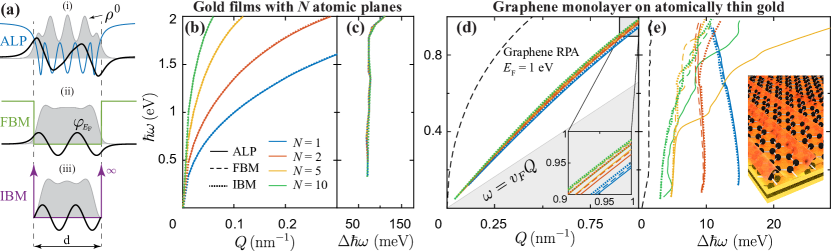
The response of the metal layer is however sensitive to the proximity of the graphene. As we show below, this demands an accurate description of its nonlocal response. To this end, we adopt a QM model for the metal layer consisting in calculating its transmission and reflection coefficients within the RPA. Full details of the formalism are provided in the Appendix. In brief, the response of valence electrons is incorporated by calculating the non-interacting RPA susceptibility from the one-electron wave functions, while polarization of inner bands is accounted for through a local screened interaction. We further assume in-plane translational symmetry, so that the valence electron wave functions can be written as , labeled by the 2D in-plane electron wave vector and the out-of-plane band index . The wave function component is obtained upon solution of the one-dimensional (1D) Schrödinger equation along the out-of-plane direction, specified for a confining potential . We focus on gold and silver, for which a choice of effective mass is appropriate, and more precisely, we apply this procedure to films consisting of a finite number of either Au(111) or Ag(111) atomic layers (metal thickness , with interlayer spacing nm). The results of this procedure depend on the specific choice of potential , for which we use three different levels of approximation:
-
•
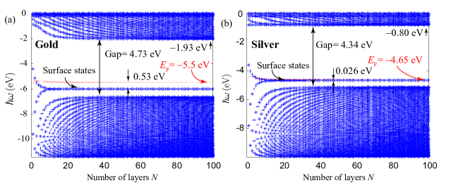
Atomic-layer potential (ALP). We adopt from Ref. Chulkov et al. (1999) a model potential that incorporates a harmonic corrugation in the bulk region and a smooth density profile at the surface, with parameters such that several important features of the electronic structure are correctly reproduced in the semi-infinite metal limit: the work function, the surface-projected bulk gap, and the position of the surface states relative to the Fermi level (see Fig. 6 in the Appendix, where the semi-infinite limit is approached for ). This potential therefore incorporates phenomenological information in a realistic fashion on (1) the out-of-plane quantization of electronic states, (2) the spill out of the electron wave functions beyond the metal film edges, and (3) the surface-projected electronic band gap produced by the bulk atomic-plane periodicity. Actually, this potential also describes surface and image states Chulkov et al. (1999), and therefore should realistically account for electron spill out effects. In practice, we designate the positions of the thin film surfaces as and , so that the first and last atomic planes are located at and , respectively (see panel (i) in Fig. 2a).
-
•
Finite-barrier model (FBM). Neglecting the atomic periodicity of the metal, we assign the potential () within the film () and otherwise (see panel (ii) in Fig. 2a), extracting the potential barrier depth from the ALP for each metal. This choice of should provide the correct offset for the obtained electron energies. The FBM describes (1) 1D quantization of electronic states and (2) electron spill out beyond the metal film edges.
-
•
Infinite-barrier model (IBM). To further simplify the model, we consider an infinite potential well such that when and elsewhere. The IBM accounts only for the quantization of electronic states along the film confinement direction.
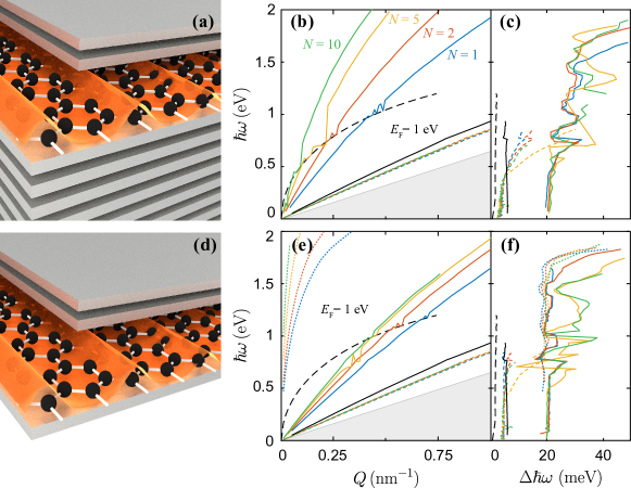
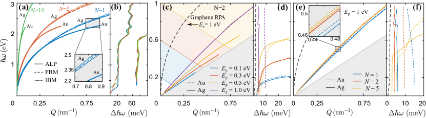
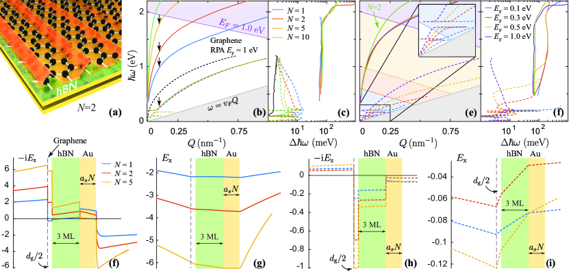
In Fig. 2b we show the SPP dispersion of self-standing gold films as predicted in the IBM, FBM, and ALP models, indicated by dotted, dashed, and solid curves, respectively, for gold films consisting of -10 atomic layers. In each case we plot the frequency corresponding to the maximum of the loss function , where is the reflection coefficient for p polarization (see Appendix) at a given in-plane optical momentum . We obtain excellent agreement among the plasmon dispersions described by each choice of binding potential within the QM model, even down to atomic-monolayer gold. We note that the dispersion curves predicted in the ALP are slightly redshifted with respect to those of the FBM, which in turn are redshifted relative to the dispersion of the IBM. Presumably, this redshift is related to electron spill out Esteban et al. (2012); David and García de Abajo (2014), although an interplay between spill out and interband polarization is known to control the actual sign of the plasmon shift for small wave vectors Liebsch (1993). The plasmon lifetime in the gold film is characterized by its spectral full width at half maximum (FWHM) plotted in Fig. 2c, as determined from the linewidth of the spectral curves; the results, which are rather independent of the choice of potential model, lie near the intrinsic phenomenological width meV introduced in the RPA formalism for gold, a value taken from a Drude model fit of optical data Johnson and Christy (1972). We find a qualitatively similar behavior in silver films, but with smaller than in gold (see Fig. 7a in the Appendix).
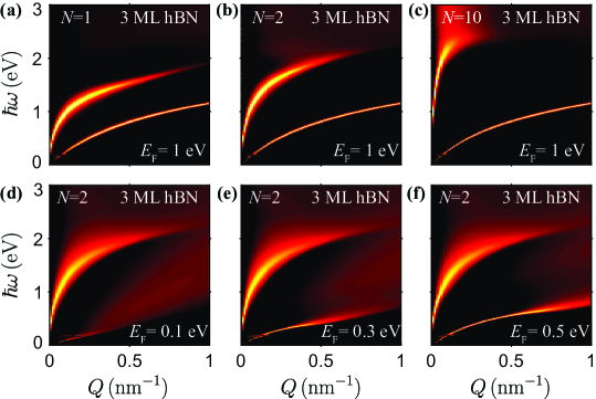
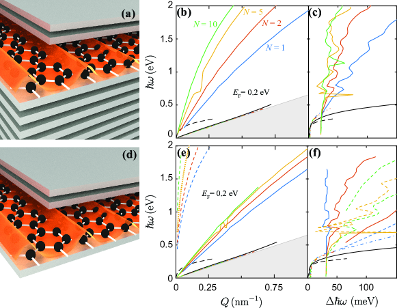
By depositing doped MG on the thin metal films, we introduce low-energy acoustic plasmon modes in the dispersion relation, for which metal screening confines light in the region between the graphene and the metal Alonso-González et al. (2017). In Fig. 2d we plot the calculated acoustic-plasmon dispersion relations for a graphene Fermi energy eV obtained by using the three QM models considered in Fig. 2b to account for the metal. Interestingly the acoustic plasmons show a dispersion that is rather independent of metal thickness down to , apart from a minor shift towards the graphene intraband region (, where m/s is the Fermi velocity in graphene) with increasing . A single atomic metal layer is thus capable of pushing the graphene plasmon dispersion (dashed curve) toward this region and render it acoustic. The associated FWHM (Fig. 2e) of the acoustic plasmon is considerably reduced compared to its higher-energy bulk counterpart (Fig. 2c) at similar wave vectors although (unlike the bulk branch the acoustic plasmon linewidth) it strongly depends on the metal thickness and the model used for the potential . It is remarkable that acoustic plasmons exist even by directly depositing the graphene on the metal without spacing, which confirms a recent prediction of this effect Principi et al. (2018), defying the intuition that metal screening can quench the graphene response. At low mid-IR frequencies, the acoustic plasmons are predicted to exhibit smaller lifetimes as the film thickness increases; thicker metal films are thus providing more efficient screening and less relative weight of the field inside the metal, where the intrinsic inelastic rate is larger than in the graphene alone (cf. dashed curve, corresponding to the assumed intrinsic lifetime fs in graphene). At higher energies, the results become more involved, as metal screening is less effective, and the FWHM depends more strongly on the model used for the potential. We remark that the ALP model, which is expected to provide the most accurate description because it incorporates several phenomenological features of the electronic band structure, leads to generally higher damping than the other models.
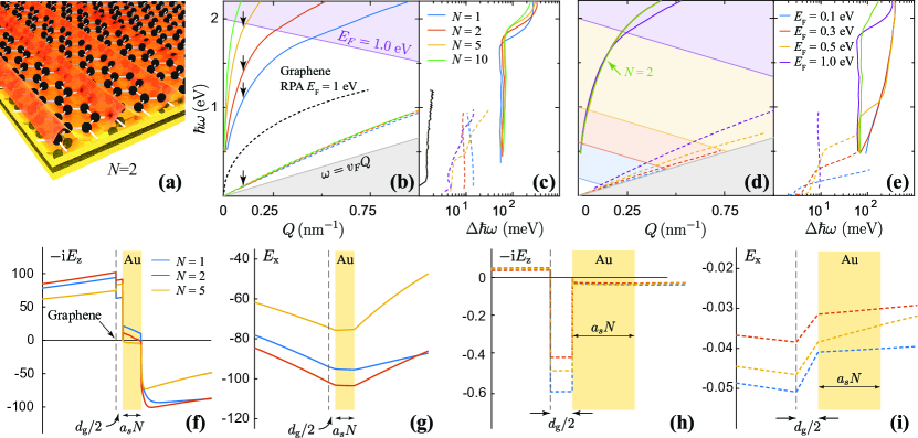
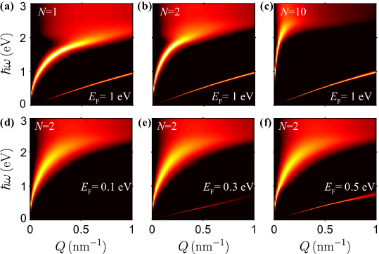
In Fig. 3 we study the full plasmon dispersion of the MG-gold film heterostructure, which is schematically illustrated in Fig. 3a for a system comprised of only two atomic gold layers (see also Fig. 8 in the Appendix for contour plots of the loss function ). Fig. 3b indicates that, while the dispersion of the acoustic plasmon is only marginally influenced by the film thickness, the higher-energy plasmon retains a similar dependence as that of the isolated film considered in Fig. 2b. At high energies approaching the interband damping regime in graphene (), the high-energy plasmon dispersion undergoes a slight redshift, accompanied by an increase in the effective plasmon damping (see Fig. 3c).
It is remarkable that the presence of a single atomic metal layer () is sufficient to support plasmons (see Figs. 2d and 3b), with a group velocity at low frequencies m/s for eV that is nearly unchanged by the addition of further atomic metal layers. These modes can be modulated by varying the Fermi energy in MG, with relatively small damping in the region, while strong attenuation is produced by interband transitions at higher energies (Fig. 3d,e).
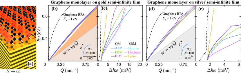
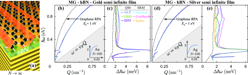
Examination of the effective damping rates in Figs. 2e and 3c indicates that an increase in film thickness can reduce the plasmon linewidth, owing to more effective screening by the metal layer. We are thus prompted to consider acoustic plasmons in the MG-gold film heterostructure in the limit of a semi-infinite metal layer, which is schematically illustrated in Fig. 4a. Our QM treatment of a thin film can also describe the response of a semi-infinite film if we approach the limit, which in practice is reached for atomic layers (see Fig. 6 in the Appendix).
We find it instructive to compare the above QM descriptions of the metal to classical approaches that are extensively used in recent literature. In particular, we consider the so-called specular-reflection model Ritchie and Marusak (1966) (SRM), also known as semiclassical infinite barrier model Ford and Weber (1984), which allows us to express the response of a semi-infinite material in terms of the nonlocal dielectric function of the bulk, while a straightforward generalization can deal with arbitrary shapes García de Abajo (2008). Following the detailed prescription presented in the Appendix, we apply this model to three different choices for the bulk dielectric response function: the hydrodynamical model Bloch (1933); Ritchie (1957), the Lindhard dielectric function Lindhard (1954); Hedin and Lundqvist (1970), and the Mermin prescription Mermin (1970). The bulk hydrodynamic model combined with the SRM coincides with the hydrodynamic model for finite geometries, which has been extensively used to discuss nonlocal effects in nanostructured metals García de Abajo (2008); McMahon et al. (2010); Mortensen et al. (2014); it incorporates nonlocal effects though the hydrodynamic pressure, as well as a phenomenological damping rate . The Lindhard dielectric function is used here with a correction intended to account for d-band screening García de Abajo (2008) (see Appendix), as well as a damping rate effectively introduced by replacing by in the Lindhard formula. The Mermin prescription corrects the Lindhard formula in order to preserve local conservation of electron density during damping processes Mermin (1970).
In Fig. 4b,c we compare the performance of the classical (i.e., SRM using hydrodynamic, Lindhard, and Mermin dielectric functions) and QM (i.e., RPA with ALP, FBM, and IBM potentials) approaches for MG deposited on an optically-thick gold surface. The dispersion relation is very similar in both cases. In contrast, we find significant discrepancies in the linewidth: the classical approach overestimates plasmon broadening when using the Lindhard and Mermin dielectric functions, but it produces a severe underestimate in the hydrodynamical model, presumably because the latter does not account for the efficient mechanism of Landau damping associated with decay into metal electron-hole pair (e-h) excitations; indeed, the bulk e-h region in gold (orange area in Fig. 4b, defined by , where the gold Fermi velocity m/s exceeds by 40% that of graphene) overlaps the plasmon dispersion for eV, where takes relatively large values. In addition to this, the finite damping introduced in the model and the lack of translational symmetry along the surface normal direction effectively extend coupling to the e-h region toward low in-plane wave vectors, thus increasing its overlap with the plasmon. Remarkably, the plasmon damping predicted by the QM approach using the IBM potential agrees well with the SRM approach using the Lindard and Mermin dielectric functions; the main difference between them lies in the neglect of quantum interference between outgoing and surface-reflected electron components in the SRM (see Appendix), which seems to play a minor role. Finally, in Fig. 4c,d we consider optically-thick silver surfaces, which exhibit qualitatively similar behavior as gold, although the reduced intrinsic inelastic damping of the argent metal ( meV) results in smaller plasmon linewidths.
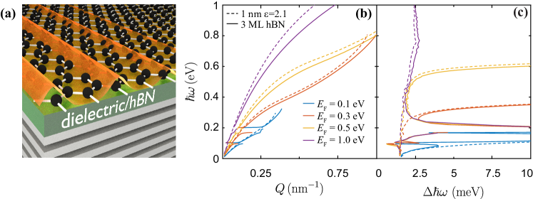
We obtain qualitatively similar results when MG is separated from the metal by a thin layer of hBN (see Figs. 9 and 10 in the Appendix). The latter introduces sharp spectral features characterized by avoided crossing between the plasmons and the mid-IR photons of the insulator. Additionally, the MG-metal interaction is reduced relative to the structures without hBN because of their larger separation, therefore yielding low-energy plasmon bands with a less acoustic character. This effect is clearly observed when comparing contour plots of the loss function in both types of structures (cf. Figs. 8 and 11 in the Appendix). Interestingly, although the acoustic plasmon dispersion depends strongly on the spacer thickness and level of graphene doping, it is not so sensitive to the permittivity of the dielectric spacer (Fig. 12 in the Appendix).
An interesting scenario arises when graphene is fully embedded in metal. We can easily simulate this type of structure through a trivial extension of the Fabry-Perot approach discussed in the Appendix. The results (Fig. 5, for graphene doped to eV and embedded in silver) reveal an interplay between three different plasmon modes provided by the graphene and each of the two metal regions. In particular, we find again an acoustic plasmon that is mainly localized in the graphene, now pushed even further toward the intraband transition region. Additionally, a higher-energy acoustic plamon emerges, and this mode becomes more acoustic and confined when one of the lower metal region is a single atomic layer (cf. Figs. 5b and 5c) because the plasmons in the two metal films are then closer in energy, so they undergo stronger interaction, similar to what we observed in Fig. 1. This second acoustic plasmon exhibits larger tunability with the number of metal atomic layers, although it is more lossy than the one dominated by graphene, as it has more weight in the metal, which is taken to have a lower intrinsic inelastic lifetime (31 fs for silver Johnson and Christy (1972)) than graphene (500 fs). Similar conclusions are observed for lower graphene doping (see Fig. 13 in the Appendix, where we consider eV).
III Conclusion
The acoustic plasmons supported by monolayer graphene when it is deposited on noble metal surfaces are strongly influenced by the metal optical response. We have identified quantum finite-size effects in the optical response of ultrathin films and semi-infinite metal layers that impact the acoustic plasmons formed by interaction with doped graphene. Remarkably, a single atomic metal layer is capable of rendering the graphene plasmons acoustic, displaying a group velocity for a doping eV that is nearly insensitive to the addition of more metal layers. The level of metal screening, which influences the plasmon lifetimes, is however strongly dependent on metal thickness. We further reveal the important contribution of electron-hole pairs in the metal to the plasmon damping, a fair description of which can only be achieved by incorporating details of the metal electronic band structure, electron spill out, and surface-projected bulk gaps, such as we do in this work using a computationally efficient quantum approach. The present study could be improved by using a first principles estimate of the internuclear distance in the MG-metal interface, as well as by introducing the effect of in-plane atomic corrugation, although these are computationally demanding calculations that we expect to produce only minor corrections. We anticipate that the results presented here can elucidate the role of quantum and finite-size effects in acoustic plasmons, enabling a fundamental understanding of the damping and extreme spatial confinement associated with these excitations.
Acknowledgements.
This work has been supported in part by the Spanish MINECO (MAT2017-88492-R and SEV2015-0522), the ERC (Advanced Grant 789104-eNANO), the European Commission (Graphene Flagship 696656), AGAUR (2017 SGR 1651), the Catalan CERCA Program, and Fundació Privada Cellex. A.R.E. acknowledges a grant cofounded by the Generalitat de Catalunya and the European Social Fund FEDER.Appendix A Optical response of a thin film heterostructure
We consider a multilayer hybrid film consisting of MG deposited on a metal film, from which it is separated by a thin dielectric layer. The optical response is expressed in terms of the reflection () and transmission () coefficients of the graphene layer ( g), the dielectric spacer ( d), and the metal film ( m) by describing the heterostructure as a Fabry-Perot resonator characterized by the total reflection and transmission coefficients Lin et al. (2017)
where the doubly-indexed coefficients combining graphene and the dielectric layer are defined as
| (1) | ||||
This prescription is convenient because we can use coefficients calculated for a surrounding vacuum by just taking the graphene-dielectric and dielectric-metal spacings as consisting of a zero-thickness vacuum layer. In the quasistatic limit here considered (see below), only p-polarization coefficients make a nonzero contribution. Explicit values of these coefficients are given below for graphene and hBN, accompanied by a quantum-mechanical approach to deal with the metal film, which we compare with a nonlocal classical solution in the thick-metal limit. While in the main text we disregard the dielectric spacer by imposing and , we provide in the Appendix complementary simulations including the effect of a thin hBN spacing layer between the graphene and the metal.
Appendix B Quantum-mechanical description of the metallic film
We study the linear optical response of a self-sustained metal film of thickness contained in the region within the RPA Pines and Nozières (1966), for which we construct the non-interacting susceptibility in terms of one-electron wave functions, which are in turn calculated as the solutions of an effective potential . For simplicity, we assume translational invariance along the in-plane directions (coordinates ) and adopt different models for the out-of-plane potential profile (see Fig. 2a). This allows us to express the optical response in terms of components of well-defined in-plane parallel wave vector and frequency , so we assume an implicit dependence on these variables, as well as a multiplicative factor . For example, the potential in real space-time has the form . Additionally, we ignore retardation effects because the wavelengths of the plasmons under investigation are much smaller than the light wavelength, and consequently, we study the response using electrostatic potentials. Specifically, we consider an external (incident) potential representing a source located below the film at (in practice we take ). The reflection coefficient is defined as the ratio of induced to external potentials , where an overall minus sign is introduced to make this definition coincide with the quasistatic limit of the Fresnel coefficient for p polarization. Likewise, the transmission coefficient is defined as , where the transmitted potential is evaluated at a position right above the film (we take ).
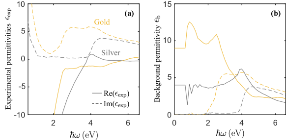
The response of inner shells is accounted for by introducing a homogeneous film of local background permittivity contained in the region, so that it extends half an atomic-layer spacing beyond each of the two outermost atomic planes (see ALP below). We note that can take relatively large values in noble metals within the visible and near-IR spectral ranges (e.g., in Au) due to d-band polarization. In practice, we obtain by subtracting from the experimentally measured metal dielectric function Johnson and Christy (1972) a Drude term, such that , where eV, eV for gold and eV, eV for silver (see Fig. 14 in the Appendix for plots of and ).
We express the total potential as
where the term accounts for the potential created by in the presence of the background slab of permittivity (i.e., including the background response, but not the response of the conduction electrons), while the integral gives the contribution due to the induced-charge density associated with disturbances in the conduction electrons. The latter is mediated by the screened interaction (i.e., the Coulomb potential created at by a point charge at oscillating with frequency in space, including the effect of background polarization). In the absence of background polarization (i.e., for ) we have , while in the presence of an film we still find a closed-form expression by direct solution of Poisson’s equation de Vega and García de Abajo (2017):
where
| (5) |
is the direct Coulomb interaction in each homogeneous region of space,
| (15) |
accounts for the effect of reflections at the film surfaces, and we define
The term captures the charge singularity in the interaction potential within each homogeneous region of space, whereas the addition of the term guarantees the continuity of the potential and the normal displacement at the interfaces. Using this expression, and noticing that the external potential originates in a source at , we can readily write the external potential including the interaction with the background film as .
Assuming linear response, we can express in terms of the susceptibility according to
where the external potential driving the free electrons has been corrected by the direct background contribution as explained above. Using matrix notation with acting as an index and a dot indicating integration over this coordinate, we can write
| (16) |
where is the non-interacting RPA susceptibility Pines and Nozières (1966). We use the well-known result Hedin and Lundqvist (1970)
| (17) |
for the full spatial dependence of this quantity in terms of the one-electron metal wave functions , where the factor of 2 accounts for spin degeneracy, is the occupation of state with energy , and denotes a phenomenological inelastic damping rate Hedin and Lundqvist (1970); Pines and Nozières (1966). In order to exploit translational invariance in the film, we multiplex the state index as , where labels eigenstates of the -dependent out-of-plane 1D Schrödinger equation defined by the noted binding potential with an effective mass (see below), while runs over 2D in-plane electron wave vectors. The electron wave functions have therefore the form , where is the film normalization area and are eigenstates of the 1D problem. Using these wave functions, we can recast Eq. (17) as , where
is the quantity actually used in Eq. (16). Here, we define occupation numbers that follow the Fermi-Dirac distribution at zero temperature for a Fermi energy , where the rightmost term inside the step function describes a parabolic dispersion along in-plane directions with effective mass as well. We evaluate these expressions by expanding all quantities in sine-Fourier transform within an embedding infinite-potential box spanning a nm vacuum region on each side of the film. The quantities , , and then become square matrices in this representation, so we operate with them using linear algebra techniques. We have further corroborated the accuracy of our numerical results by comparing with a real-space discretization in the coordinate, which further reduces spurious Gibbs’ oscillations in the calculation of the near fields, although the sine basis generally converges with a smaller number of elements.
The average volumetric electron density in the film is , where the factor of 2 is again due to spin degeneracy. Using the customary transformation , we obtain the self-consistent expression for the Fermi energy
where denotes the highest band index for which . To correctly define for arbitrary thickness, we fit the charge density in the bulk limit () by imposing experimentally-measured values of relative to vacuum in gold ( eV) and silver ( eV). The choice of potential parameters Chulkov et al. (1999) in the ALP further ensures that the binding energies of surface states agree with available experimental measurements Paniago et al. (1995) (see thickness-dependent band structure in Fig. 6 in the Appendix). Under these conditions we obtain effective charge densities nm-3 for gold and nm-3 for silver. For the sake of consistency, we use these values of in the calculations of presented in this work for all models of (see Fig. 2a), and we also assume the same density per layer for finite-thickness films.
Appendix C Nonlocal classical electromagnetic description of a semi-infinite metal film
For the sake of comparison in the thick-film limit, we adopt the SRM Ritchie and Marusak (1966); García de Abajo (2008); Pitarke et al. (2007) to compute a nonlocal reflection coefficient for a semi-infinite metal in the framework of classical electrodynamics. This model allows us to relate the surface response to the momentum- and frequency-dependent dielectric function of the metal under the assumption that conduction electrons undergo specular reflection at the surface without quantum interference between outgoing and reflected components. In practical terms, we calculate the reflection coefficient in the SRM as Ritchie and Marusak (1966); García de Abajo (2008)
where
plays the role of a surface response function. We further decompose the bulk metal permittivity as García de Abajo (2008) , where is the local background response defined above (see Fig. S9 in the Appendix) and describes the nonlocal contribution of free conduction electrons. We adopt three different levels of approximation for the latter in the calculations presented in Fig. 4:
where the subscripts refer to the hydrodynamic Bloch (1933); Ritchie (1957), Lindhard Lindhard (1954); Hedin and Lundqvist (1970), and Mermin Mermin (1970) models (see main text). Here, is the bulk plasma frequency of the metal, is the Fermi energy, is the Fermi wave vector expressed in terms of the one-electron radius , and we use the function
Incidentally, the reflection coefficient derived from the SRM combined with the choice coincides with the solution of the classical hydrodynamic equations García de Abajo (2010), where the term accounts for the hydrodynamic pressure. We apply these models to gold and silver by taking and Bohr-radius (i.e., nm), as well as values for and as specified above.
Appendix D Reflection and transmission coefficients of monolayer graphene
We adopt the well-known expressions for the reflection and transmission coefficients of a zero-thickness 2D graphene monolayer in the quasistatic limit García de Abajo (2014)
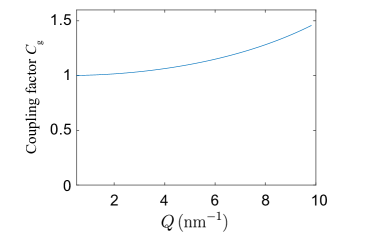
where is the wave-vector- and frequency-dependent nonlocal conductivity of graphene, which we evaluate in the RPA Wunsch et al. (2006); Hwang and Sarma (2007), further introducing an inelastic lifetime fs via Mermin’s prescription Mermin (1970). Incidentally, applying Eq. (1) to the above graphene transmission and reflection coefficients, combined with the coefficients and for the planar surface of a dielectric of permittivity , we readily obtain the coefficient with for internal reflection from graphene supported by the dielectric, used in the tutorial model presented in the discussion of Fig. 1. In order to account for the finite extension of the carbon 2p orbitals outward from the plane of the graphene monolayer, we introduce effective graphene reflection and transmission coefficients and , where nm is the interlayer spacing of graphite and is a coupling factor defined as
We approximate by using a tabulated 2p orbital for an isolated carbon atom Clementi and Roetti (1974). More precisely, , where , , , , , , , and , all in atomic units. The result is plotted in Fig. 15, where we find at in virtue of orbital normalization. The assumption of an effective thickness implies that classically there is always a finite separation between the carbon nuclei plane in graphene and the surrounding media.
Appendix E Optical response of a hBN film
Motivated by recent experimental studies, we present in the Appendix calculations for systems in which the MG and the metal film are separated by a thin layer of hBN (see Figs. 9 and 10). The hBN region is taken to have a thickness corresponding to an integer number of atomic-layer spacings along the out-of-plane c(1111) direction. We describe this layer through a local anisotropic permittivity with tensor components Geick et al. (1966)
for parallel () or perpendicular () directions relative to the atomic layers. Here, runs over oscillators (Lorentzians) with resonance energies , , , ; transition strengths , , , ; and dampings , , , (all of them in meV). Following the methods of Ref. de Vega and García de Abajo (2017), we readily obtain the reflection and transmission coefficients
where (with ) and (with ). In the calculations presented in the Appendix, we assume a thickness nm, corresponding to 3 MLs of hBN Golla et al. (2013).
Appendix F Atomic layer potential (ALP)
In the ALP model we use the parametrized potential of Ref. Chulkov et al. (1999) to obtain the one-electron states of a metal film including ad hoc band-structure information. Specifically, this potential consists of a harmonic bulk component, a differentiated region describing each outermost layer, and a long-range image tail, constructed in such a way that it reproduces several experimentally observed electronic structure features, namely: the work function, the surface-projected bulk gap, and the position of the surface states relative to the Fermi level, all of which depend on material and crystallographic orientation. For simplicity and to a good approximation, we take the effective electron mass as in all directions. For a semi-infinite metal placed in the region, the potential referred to the vacuum level can be written as Chulkov et al. (1999)
| (22) |
where the normal coordinate is given relative to the position of the outermost atomic plane (); is the inter-atomic layer spacing; the coefficients and are chosen to reproduce the width and position of the noted energy gap, respectively; the space between and represents the transition from the solid bulk to free-space, where electron spill out takes place; and the parameters and determine the positions of the Fermi level and the surface states relative to the vacuum level. We list the values of these parameters for Au(111) and Ag(111) in Table 1. Five of the remaining six parameters are determined by imposing the continuity of the potential and its first derivative, so that , , , , and , while the intermediate point is fixed with respect to the surface atomic layer in such a way that corresponds to the image plane position, which is important for describing image states Chulkov et al. (1999). The potential for a film with outermost atomic planes at and can be expressed using Eq. (22) as
| (25) |
which is continuous at by construction. Obviously, must be taken to be a multiple of the atomic-layer spacing .
Appendix G Additional figures
References
- Novoselov et al. (2004) K. S. Novoselov, A. K. Geim, S. V. Morozov, D. Jiang, Y. Zhang, S. V. Dubonos, I. V. Grigorieva, and A. A. Firsov, Science 306, 666 (2004).
- Xia et al. (2014) F. Xia, H. Wang, D. Xiao, M. Dubey, and A. Ramasubramaniam, Nat. Photon. 8, 899 (2014).
- Alcaraz Iranzo et al. (2018) D. Alcaraz Iranzo, S. Nanot, E. J. C. Dias, I. Epstein, C. Peng, D. K. Efetov, M. B. Lundeberg, R. Parret, J. Osmond, J.-Y. Hong, et al., Science 360, 291 (2018).
- Cox and García de Abajo (2014) J. D. Cox and F. J. García de Abajo, Nat. Commun. 5, 5725 (2014).
- Lee and El-Sayed (2006) K.-S. Lee and M. A. El-Sayed, J. Phys. Chem. B 110, 19220 (2006).
- Geim and Grigorieva (2013) A. K. Geim and I. V. Grigorieva, Nature p. 419 (2013).
- Basov et al. (2016) D. N. Basov, M. M. Fogler, and F. J. García de Abajo, Science 354, aag1992 (2016).
- Economou (1969) E. N. Economou, Phys. Rev. 182, 539 (1969).
- Barnes et al. (2003) W. L. Barnes, A. Dereux, and T. W. Ebbesen, Nature 424, 824 (2003).
- Mulvaney et al. (2006) P. Mulvaney, J. Pérez-Juste, M. Giersig, L. M. Liz-Marzán, and C. Pecharromán, Plasmonics 1, 61 (2006).
- Khurgin (2015) J. B. Khurgin, Nat. Nanotech. 10, 2 (2015).
- Fei et al. (2011) Z. Fei, G. O. Andreev, W. Bao, L. M. Zhang, A. S. McLeod, C. Wang, M. K. Stewart, Z. Zhao, G. Dominguez, M. Thiemens, et al., Nano Lett. 11, 4701 (2011).
- Chen et al. (2012) J. Chen, M. Badioli, P. Alonso-González, S. Thongrattanasiri, F. Huth, J. Osmond, M. Spasenović, A. Centeno, A. Pesquera, P. Godignon, et al., Nature 487, 77 (2012).
- Fei et al. (2012) Z. Fei, A. S. Rodin, G. O. Andreev, W. Bao, A. S. McLeod, M. Wagner, L. M. Zhang, Z. Zhao, M. Thiemens, G. Dominguez, et al., Nature 487, 82 (2012).
- Woessner et al. (2015) A. Woessner, M. B. Lundeberg, Y. Gao, A. Principi, P. Alonso-González, M. Carrega, K. Watanabe, T. Taniguchi, G. Vignale, M. Polini, et al., Nat. Mater. 14, 421 (2015).
- Ni et al. (2018) G. X. Ni, A. S. McLeod, Z. Sun, L. Wang, L. Xiong, K. W. Post, S. S. Sunku, B.-Y. Jiang, J. Hone, C. R. Dean, et al., Nature 557, 530 (2018).
- García de Abajo (2014) F. J. García de Abajo, ACS Photon. 1, 135 (2014).
- Emani et al. (2012) N. K. Emani, T.-F. Chung, X. Ni, A. V. Kildishev, Y. P. Chen, and A. Boltasseva, Nano Lett. 12, 5202 (2012).
- Yu et al. (2016) R. Yu, V. Pruneri, and F. J. García de Abajo, Sci. Rep. 6, 32144 (2016).
- Lundeberg et al. (2017) M. B. Lundeberg, Y. Gao, R. Asgari, C. Tan, B. V. Duppen, M. Autore, P. Alonso-González, A. Woessner, K. Watanabe, T. Taniguchi, et al., Science 89, 035004 (2017).
- Iranzo et al. (2018) D. A. Iranzo, S. Nanot, E. J. C. Dias, I. Epstein, C. Peng, D. K. Efetov, M. B. Lundeberg, R. Parret, J. Osmond, J.-Y. Hong, et al., Science 360, 291 (2018).
- Dionne et al. (2006) J. A. Dionne, L. A. Sweatlock, H. A. Atwater, and A. Polman, Phys. Rev. B 73, 035407 (2006).
- Principi et al. (2011) A. Principi, R. Asgari, and M. Polini, Solid State Commun. 151, 1627 (2011).
- Principi et al. (2018) A. Principi, E. van Loon, M. Polini, and M. I. Katsnelson, Phys. Rev. B 98, 035427 (2018).
- Dias et al. (2018) E. J. C. Dias, D. A. Iranzo, P. A. D. Gonçalves, Y. Hajati, Y. V. Bludov, A.-P. Jauho, N. A. Mortensen, F. H. L. Koppens, and N. M. R. Peres, Phys. Rev. B 97, 245405 (2018).
- Bloch (1933) F. Bloch, Z. Phys. 81, 363 (1933).
- Ritchie (1957) R. H. Ritchie, Phys. Rev. 106, 874 (1957).
- David and García de Abajo (2014) C. David and F. J. García de Abajo, ACS Nano 8, 9558 (2014).
- Mortensen et al. (2014) N. A. Mortensen, S. Raza, M. Wubs, T. Søndergaard, and S. I. Bozhevolnyi, Nat. Commun. 5, 3809 (2014).
- Raza et al. (2013a) S. Raza, T. Christensen, M. Wubs, S. I. Bozhevolnyi, and N. A. Mortensen, Phys. Rev. B 88, 115401 (2013a).
- Moreau et al. (2013) A. Moreau, C. Ciracì, and D. R. Smith, Phys. Rev. B 87, 045401 (2013).
- David et al. (2013) C. David, N. A. Mortensen, and J. Christensen, Sci. Rep. 3, 2526 (2013).
- Ciraci et al. (2013) C. Ciraci, J. B. Pendry, and D. R. Smith, Chem. Phys. Chem 14, 1109 (2013).
- David and Christensen (2017) C. David and J. Christensen, Appl. Phys. Lett. 110, 261110 (2017).
- Jaklevic and Lambe (1975) R. C. Jaklevic and J. Lambe, Phys. Rev. B 12, 4146 (1975).
- Hövel et al. (2010) M. Hövel, B. Gompf, and M. Dressel, Phys. Rev. B 81, 035402 (2010).
- Qian et al. (2015) H. Qian, Y. Xiao, D. Lepage, L. Chen, and Z. Liu, Nanophotonics 4, 413 (2015).
- Raza et al. (2013b) S. Raza, T. Christensen, M. Wubs, S. I. Bozhevolnyi, and N. A. Mortensen, Phys. Rev. B 88, 115401 (2013b).
- Bondarev and Shalaev (2017) I. V. Bondarev and V. M. Shalaev, Opt. Mater. Express 7, 3731 (2017).
- Runge and Gross (1984) E. Runge and E. K. U. Gross, Phys. Rev. Lett. 52, 997 (1984).
- Pitarke et al. (2007) J. M. Pitarke, V. M. Silkin, E. V. Chulkov, and P. M. Echenique, Rep. Prog. Phys. 70, 1 (2007).
- Yan et al. (2011) J. Yan, K. W. Jacobsen, and K. S. Thygesen, Phys. Rev. B 84, 235430 (2011).
- Laref et al. (2013) S. Laref, J. Cao, A. Asaduzzaman, K. Runge, P. Deymier, R. W. Ziolkowski, M. Miyawaki, , and K. Muralidharan, Opt. Express 21, 11827 (2013).
- Schiller et al. (2014) F. Schiller, Z. M. A. El-Fattah, S. Schirone, J. Lobo-Checa, M. Urdanpilleta, M. Ruiz-Osés, J. Cordón, M. Corso, D. Sánchez-Portal, A. Mugarza, et al., New J. Phys. 16, 123025 (2014).
- Sundararaman et al. (2018) R. Sundararaman, T. Christensen, Y. Ping, N. Rivera, J. D. Joannopoulos, M. Soljačić, and P. Narang, p. arXiv:1806.02672 (2018).
- Shah et al. (2018) D. Shah, A. Catellani, H. Reddy, N. Kinsey, V. Shalaev, A. Boltasseva, and A. Calzolari, ACS Photon. 5, 2816 (2018).
- Johnson and Christy (1972) P. B. Johnson and R. W. Christy, Phys. Rev. B 6, 4370 (1972).
- Jackson (1999) J. D. Jackson, Classical Electrodynamics (Wiley, New York, 1999).
- García de Abajo and Manjavacas (2015) F. J. García de Abajo and A. Manjavacas, Faraday Discuss. 178, 87 (2015).
- Profumo et al. (2012) R. E. V. Profumo, R. Asgari, M. Polini, and A. H. MacDonald, Phys. Rev. B 85, 085443 (2012).
- Wunsch et al. (2006) B. Wunsch, T. Stauber, F. Sols, and F. Guinea, New J. Phys. 8, 318 (2006).
- Hwang and Das Sarma (2007) E. H. Hwang and S. Das Sarma, Phys. Rev. B 75, 205418 (2007).
- Silveiro et al. (2015) I. Silveiro, J. M. Plaza Ortega, and F. J. García de Abajo, Light Sci. Appl. 4, e241 (2015).
- Chulkov et al. (1999) E. Chulkov, V. Silkin, and P. Echenique, Surf. Sci. 437, 330 (1999).
- Esteban et al. (2012) R. Esteban, A. G. Borisov, P. Nordlander, and J. Aizpurua, Nat. Commun. 3, 825 (2012).
- Liebsch (1993) A. Liebsch, Phys. Rev. B 48, 11317 (1993).
- Alonso-González et al. (2017) P. Alonso-González, A. Y. Nikitin, Y. Gao, A. Woessner, M. B. Lundeberg, A. Principi, N. Forcellini, W. Yan, Saül, A. J. Huber, et al., Nat. Nanotech. 12, 31 (2017).
- Ritchie and Marusak (1966) R. H. Ritchie and A. L. Marusak, Surf. Sci. 4, 234 (1966).
- Ford and Weber (1984) G. W. Ford and W. H. Weber, Phys. Rep. 113, 195 (1984).
- García de Abajo (2008) F. J. García de Abajo, J. Phys. Chem. C 112, 17983 (2008).
- Lindhard (1954) J. Lindhard, K. Dan. Vidensk. Selsk. Mat. Fys. Medd. 28, 1 (1954).
- Hedin and Lundqvist (1970) L. Hedin and S. Lundqvist, in Solid State Physics, edited by D. T. Frederick Seitz and H. Ehrenreich (Academic Press, 1970), vol. 23 of Solid State Physics, pp. 1 – 181.
- Mermin (1970) N. D. Mermin, Phys. Rev. B 1, 2362 (1970).
- McMahon et al. (2010) J. M. McMahon, S. K. Gray, and G. C. Schatz, Nano Lett. 10, 3473 (2010).
- Lin et al. (2017) I.-T. Lin, C. Fan, and J.-M. Liu, IEEE J. Sel. Top. Quant. Electr. 23, 144 (2017).
- Pines and Nozières (1966) D. Pines and P. Nozières, The Theory of quantum liquids (W. A. Benjamin, Inc., New York, 1966).
- de Vega and García de Abajo (2017) S. de Vega and F. J. García de Abajo, ACS Photon. 4, 2367 (2017).
- Paniago et al. (1995) R. Paniago, R. Matzdorf, G. Meister, and A. Goldmann, Surf. Sci. 336, 113 (1995).
- García de Abajo (2010) F. J. García de Abajo, Rev. Mod. Phys. 82, 209 (2010).
- Hwang and Sarma (2007) E. H. Hwang and S. D. Sarma, Phys. Rev. B 75, 205418 (2007).
- Clementi and Roetti (1974) E. Clementi and C. Roetti, At. Data Nucl. Data Tables 14, 177 (1974).
- Geick et al. (1966) R. Geick, C. H. Perry, and G. Rupprecht, Phys. Rev. 146, 543 (1966).
- Golla et al. (2013) D. Golla, K. Chattrakun, K. Watanabe, T. Taniguchi, B. J. LeRoy, and A. Sandhu, Appl. Phys. Lett. 102, 161906 (2013).
- Kevan and Gaylord (1987) S. D. Kevan and R. H. Gaylord, Phys. Rev. B 36, 5809 (1987).
- Zeman and Schatz (1987) E. J. Zeman and G. C. Schatz, J. Phys. Chem. 91, 634 (1987).