Tomonaga-Luttinger liquid in the edge channels of a quantum spin Hall insulator
Topological quantum matter is characterized by non-trivial global invariants of the bulk which induce gapless electronic states at its boundaries. A case in point are two-dimensional topological insulators (2D-TI) which host one-dimensional (1D) conducting helical edge states protected by time-reversal symmetry (TRS) against single-particle backscattering (SPB). However, as two-particle scattering is not forbidden by TRS Xu and Moore (2006), the existence of electronic interactions at the edge and their notoriously strong impact on 1D states may lead to an intriguing interplay between topology and electronic correlations. In particular, it is directly relevant to the question in which parameter regime the quantum spin Hall effect (QSHE) expected for 2D-TIs becomes obscured by these correlation effects that prevail at low temperatures Li et al. (2015). Here we study the problem on bismuthene on SiC(0001) which has recently been synthesized and proposed to be a candidate material for a room-temperature QSHE Reis et al. (2017). By utilizing the accessibility of this monolayer-substrate system on atomic length scales by scanning tunneling microscopy/spectroscopy (STM/STS) we observe metallic edge channels which display 1D electronic correlation effects. Specifically, we prove the correspondence with a Tomonaga-Luttinger liquid (TLL), and, based on the observed universal scaling of the differential tunneling conductivity (), we derive a TLL parameter reflecting intermediate electronic interaction strength in the edge states of bismuthene. This establishes the first spectroscopic identification of 1D electronic correlation effects in the topological edge states of a 2D-TI.
The topological protection of the 1D metallic edge channels in 2D-TIs against elastic SPB by TRS Kane and Mele (2005a, b) leads to quantized, i.e. dissipationless transport which is reflected in the QSHE. Moreover, the property of spin-momentum locking renders 2D-TIs promising candidate materials for applications in spintronics. To date, the QSHE has only been measured in three material systems that are all characterized by small bandgaps () of which the quantum well (QW) structures of three-dimensional semiconductors, such as HgTe/CdTe König et al. (2007) and InAs/GaSb Knez et al. (2011), constitute the most prominent realizations. Recently, the QSHE effect has been reported to be observed up 100 K in monolayer crystals of WTe2 Wu et al. (2018); Tang et al. (2017). While most of these experiments can be well-understood within topological band theory of non-interacting electrons, the deviations from a sharply quantized conductance () seen at very low temperatures in InAs/GaSb QW transport measurements have been attributed to the relevance of electronic interactions Li et al. (2015). In fact, in any real 2D-TI such interactions are inevitably present and will play a non-negligible role for the 1D edge states which are consequently expected to constitute a helical TLL. Wu et al. (2006); Xu and Moore (2006) A direct spectroscopic identification of this correlated many-body state in the edge states of a 2D-TI, however, has remained lacking so far.
Bismuthene, i.e. a 2D monolayer of Bi atoms epitaxially grown on a semiconducting SiC(0001) substrate, turns out to be a particularly well-suited system for such studies. Here the strong atomic spin-orbit coupling in the Bi atoms conspires with their honeycomb arrangement and covalent coupling to the substrate to drive the system into a non-trivial topology Reis et al. (2017); Li et al. (2018). Angle-resolved photoelectron spectroscopy as well as STM/STS found excellent agreement with the calculated non-trivial topological band structure Reis et al. (2017) and confirmed a sizable fundamental band gap (), potentially allowing the persistence of the QSHE up to room-temperature and beyond. Moreover, STM/STS measurements clearly indicate the existence of conducting edge channels which due to the large bulk band gap display an extremely small exponential decay length into the insulating 2D bulk of only Reis et al. (2017).
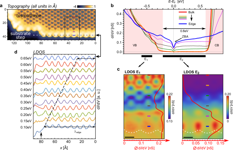
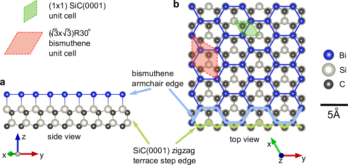
The near-to-perfect spatial 1D confinement of the metallic edge states is ideally matched to the atomic resolution of STM/STS, as illustrated Fig. 1. While with constant current STM we are able to explore the surface topography, STS allows us to spatially map the local electronic density of states (LDOS). Accordingly, the STM topography map in Fig. 1(a) demonstrates the successful synthesis of bismuthene with its planar atomic honeycomb structure. While bismuthene covers SiC smoothly within substrate terraces, the monolayer film is truncated at SiC zigzag terrace steps. Due to the superstructure of the Bi honeycomb lattice with respect to the substrate, this translates into well-ordered armchair edges of the bismuthene layer (see Fig. 1(a) and Fig. S1). We note that the periodic spacing between the bright white, oval edge features in Fig. 1(a) is in agreement with theoretical expectations for armchair edges and indicates the accumulation of charge density at the edge.
This assumption is supported by the STS LDOS data. While the differential conductivity measured well inside the bulk material (Fig. 1(b), red curve) is dominated by the bulk bismuthene band gap, it becomes continuously filled as the tunneling tip moves towards the film edge (thin curves in Fig. 1(b)). Eventually, directly at the edge (blue curve in Fig.1(b)) the differential conductivity indicates a nearly constant LDOS, except for the apparent dip around indicated by ’ZBA’ and discussed further below. Spatially resolved -maps taken parallel to the bismuthene edge (Fig. 1(c)) further elucidate the 1D character of the edge LDOS. Within the occupied states, e.g., in the energy range , the bismuthene bulk LDOS can be seen clearly. Evidently the edge LDOS has already set in. In contrast, inside the bulk energy gap the LDOS is confined solely to the geometrical edge, defining a highly constricted 1D metallic channel spreading along the entire extent of the SiC terrace step edge ( – ). (See movie in supplementary information for full evolution of the edge LDOS with energy.)
We notice that the edge in Fig. 1(a) encompasses a kink in the substrate step. For an ordinary 1D electron wave one would expect a partial reflection off the kink causing a quasi-particle interference with the incident wave. Such emerging Friedel oscillations would scale with the energy-dependent electron wavelength defined by the band dispersion. Reis et al. (2017) Eventually, the electrons in an ordinary 1D conductor may even become localized depending on the strength of the potential scatterer Meyer et al. (2003). However, in our case the periodicity seen in the edge LDOS is exclusively caused by the topographic, i.e. atomic modulation of the armchair edge, irrespective of electron energy as can clearly be seen in Fig. 1(d). Most importantly, no energy-dependent Friedel oscillations are observed, consistent with the topological protection of the helical edge states in a 2D-TI against SPB. Consequently, the effective mean free path of the edge channels is extraordinarily large, as kinks and (non-magnetic) impurity potentials do not act as scattering centers Pauly et al. (2015).
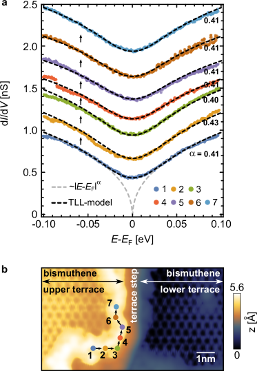
The LDOS of a (metallic) Fermi liquid is expected to be finite and nearly constant around the Fermi level. In contrast, our edge state spectra display a clearly detectable dip at which in the following will be referred to as zero-bias anomaly (ZBA). In an energy window of around it displays particle-hole symmetric behavior following (not too close to ) a power-law with as high-resolution single-point STS reveals in Fig. 2(a). Interestingly, spectral shape and power law exponent of the ZBA persist along the entire length of the 1D edge channel and do not even change as one follows the LDOS around a strongly kinky section of the edge (see Fig. 2(b) for measurement path), reminiscent of the absence of SPB at the edge kinks.
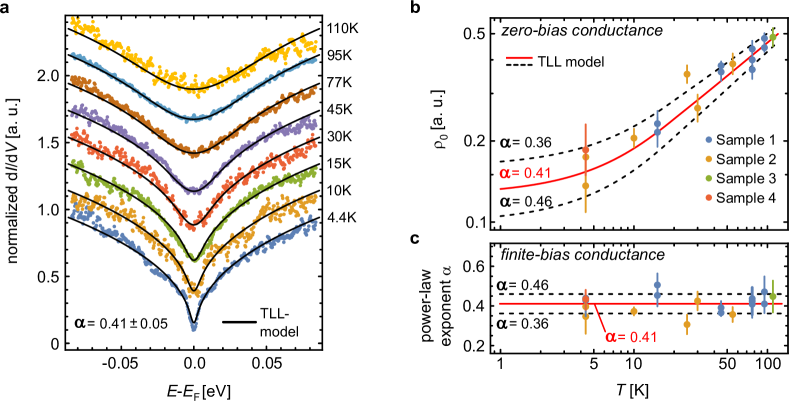
The ZBA also features a pronounced temperature dependence, see Fig. 3(a). As the temperature increases from to the zero energy dip gets continuously filled. For further quantitative analysis Fig. 3(b) shows the normalized zero-bias differential conductivity as a function of temperature on a double logarithmic scale. It is apparent that for the zero-bias differential conductivity again follows a power-law , with the same exponent already observed in the energy dependence. For deviations from the bare power-law are due to instrumental broadening. The finite bias differential conductivity, on the other hand, and especially the energy power law remains constant as a function of temperature (see Fig.3(c)).
It is well-established that electronic interactions play a crucial role in 1D metallic systems. As described by TLL theory, the Fermi liquid description breaks down in 1D and the physics is dominated by collective bosonic excitations Voit (1993); Haldane (1981). Signatures of ordinary (spinful) TLLs have been observed, e.g., in semiconducting GaAs quantum wires Jompol et al. (2009), metallic single wall carbon nanotubes Bockrath et al. (1999), in polymer nanofibers Aleshin et al. (2004), and atomic chains of gold atoms on Ge surfaces Blumenstein et al. (2011). TLL behavior has also been identified in the chiral edge states of fractional quantum Hall systems Chang et al. (1996). A special case are the spin-momentum-locked edge states in a 2D-TI which form a helical TLL as long as the electronic interaction is weaker than the band gap that protects them from the 2D bulk states Hohenadler and Assaad (2012). However, one common characteristic inherent to all (spinful and helical) TLLs is a power-law behavior of their single-particle spectrum, for Braunecker et al. (2012), directly accessible by experimental electron removal and addition spectroscopies, such as STS Eggert (2000). In fact, the energy dependence emerges from an even more fundamental property of TLLs, namely the universal scaling in both energy and temperature which is captured by the expression Bockrath et al. (1999):
| (1) |
This inherently generates also a temperature power-law dependence of the zero energy spectral weight with the same exponent as in energy. Comparing with our experimental STS data we find excellent agreement with the theoretical over the entire energy and temperature range as seen in Fig. 2(a) and Fig. 3(a)(black curves), suggesting that the ZBA observed in the edge states is indeed due to strong 1D electron corrrelations.
However, the TLL interpretation has to be discriminated against other possible origins of a ZBA. One scenario is the Efros-Shklovskii pseudogap which can arise from the interplay of disorder and Coulomb interaction in low-dimensional metallic systems. It is characterized by an exponential suppression of the LDOS Bartosch and Kopietz (2002). As the observed ZBA in bismuthene follows a power-law instead, the disorder-induced pseudogap can be safely excluded (see also Fig. S5 for a direct comparison). Another mechanism that can lead to a suppression of the low-energy tunneling is the dynamical Coulomb blockade (DCB) Hanna and Tinkham (1991); Devoret et al. (1990) caused by the interplay between charge storage energy in and charge dissipation from a nanostructure (here the 1D edge). Within environment-quantum fluctuation or -theory this can be treated by modeling the STS tunneling junction as a capacitance parallel to a resistance . For and at zero temperature a power-law behavior is predicted according to with the exponent Devoret et al. (1990), being the resistance quantum. We have measured the ZBA on four different samples, on bismuthene domains with differing sizes, and with widely varied set-point parameters and (see Fig. S4), where the local tunnel junction parameters and should widely differ accordingly. Yet, in all cases we observe the same power law exponent , at variance with the DCB picture. Finally, universal scaling would not be observed in the DCB scenario for the same locality reasons Ming et al. (2018).
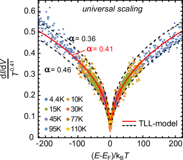
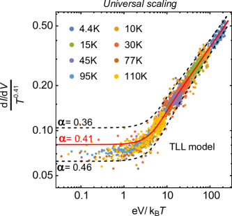
On the other hand, universal scaling can be directly tested for our tunneling spectra. In Fig. 4 the experimental data are normalized to and plotted versus . Unambiguously all spectra collapse onto a single universal curve (red curve) as predicted for a TLL according to Eq. (1) Bockrath et al. (1999); Blumenstein et al. (2011). Our observation leads to the conclusion that the ZBA is a result of intrinsic properties of the 1D edge channel and cannot arise from the DCB scenario. Ultimately, our observations provide critical proof to render bismuthene the first 2D-TI system for which a TLL behavior has been established and studied on the atomic scale. Moreover, the absence of Friedel oscillations is in agreement with the TLL in bismuthene being helical.
Within TLL theory the strength of the Coulomb interaction between the electrons in the 1D edge channel can be expressed by the parameter , where is the Fermi velocity. For non-interacting electrons . Moderate to strong electronic interactions result in two-particle scattering in the edge channels of the 2D-TI (see Ref. Xu and Moore (2006); Wu et al. (2006)), rendering essential for the interpretation of transport measurements on 2D-TIs. To date, only few experimental studies have addressed the effect of electronic correlations in the edge channels. A notable exception is a recent transport study of InAs/GaSb QWs which reported experimental evidence for a helical TLL Li et al. (2015). However, the extraction of from transport data is ambiguous, because the resulting values vary widely depending on the underlying theory ( Li et al. (2015) vs. Väyrynen et al. (2016)). Many authors propose a more direct determination of by local spectroscopy (i.e. STS) of the electronic spectral function Eggert (2000); Blumenstein et al. (2011); Bockrath et al. (1999). Accordingly, for a helical TLL the characteristic power-law exponent of the generic spectrum (1) is directly related to via (note the prefactor which for a spinful TLL would be Braunecker et al. (2012)). The experimentally determined exponent thus translates into the helical TLL parameter for the bismuthene armchair edge channels.
Qualitatively, the effective electronic interaction strength is expected to be enhanced (reduced) with decreasing (increasing) Fermi velocity and confinement length of the 1D edge channels. For example, for HgTe/CdTe QWs (m/s, nm) theoretical estimates yield (Ref. Teo and Kane (2009)), placing this system in the weakly to nearly non-interacting regime. In contrast, for bismuthene the key parameters are and Reis et al. (2017). Such exceptionally narrow confinement length (2 orders of magnitude less than in HgTe/CdTe QWs) is driven by the large bulk gap of in bismuthene (). This suggests a substantially stronger interaction, which is nicely confirmed by our experimental value . It is further underpinned by a theoretical model for bismuthene which results in (see supplementary information).
Bismuthene on SiC is thus the first 2D-TI candidate in which
the spectral properties of a (helical) TLL have been verified
in its 1D edge states. The experimentally determined
helical TLL parameter indicates that the edge channels – while
topologically protected against SPB –
display pronounced two-particle scattering. With regard to the QSHE, bismuthene
is thus a model system to study in which way the conductance quantization is affected by these
correlation effects.
Methods
Bismuthene was grown on n-doped 4H-SiC(0001) substrates with a resistivity of at room-temperature. The dopant concentration of the substrate is . The STM/STS measurements have been performed with a commercial low-temperature
STM from Scienta Omicron GmbH under UHV conditions (). Topographic STM images are recorded as constant current
images. After stabilizing the tip at a voltage and current set-point
and , respectively, the feedback loop is opened and
STS spectra are obtained making additional use of a standard lock-in technique
with a modulation frequency of and modulation amplitude
. Because of external modulation the
instrumental resolution results in an gaussian energy broadening (FWHM: ) in addition to the thermal broadening caused by
the Fermi-Dirac function (FWHM ). We only show single-point spectra
and avoid averaging over various STS spectra of a finite sample area.
Prior to every measurement on bismuthene we assured that the
tip LDOS is metallic and to a good approximation can be considered constant in
the energy range by a reference measurement on a silver surface.
As a result, curves measured with this tip are a good measure of the
sample LDOS.
Acknowledgements
We thank B. Trauzettel, A. Kowalewski and J. Maciejko for useful
discussions. This work was supported by the Deutsche Forschungsgemeinschaft
(DFG) through the Collaborative Research Center SFB 1170
”ToCoTronics” in Würzburg, the SPP 1666 Priority Program
”Topological Insulators”, and by the European Research Council (ERC) through starting
grant ERC-StG-Thomale-336012 ”Topolectrics”.
Author contributions R.S. and F.R. carried out the measurements, R.S. analysed the data and made the figures. T.M., T.H., T.S, and R.T. developed the theory for the helical edge with dielectric screening. J.S. conceived the experiment. R.S. and R.C. wrote the text with input from J.S. and F.R., and all authors contributed to critical discussion of the data.
References
- Xu and Moore (2006) C. Xu and J. E. Moore, Phys. Rev. B 73, 045322 (2006).
- Li et al. (2015) T. Li, P. Wang, H. Fu, L. Du, K. A. Schreiber, X. Mu, X. Liu, G. Sullivan, G. A. Csáthy, X. Lin, and R.-R. Du, Phys. Rev. Lett. 115, 136804 (2015).
- Reis et al. (2017) F. Reis, G. Li, L. Dudy, M. Bauernfeind, S. Glass, W. Hanke, R. Thomale, J. Schäfer, and R. Claessen, Science 357 (2017).
- Kane and Mele (2005a) C. L. Kane and E. J. Mele, Phys. Rev. Lett. 95, 226801 (2005a).
- Kane and Mele (2005b) C. L. Kane and E. J. Mele, Phys. Rev. Lett. 95, 146802 (2005b).
- König et al. (2007) M. König, S. Wiedmann, C. Brüne, A. Roth, H. Buhmann, L. W. Molenkamp, X.-L. Qi, and S.-C. Zhang, Science 318, 766 (2007).
- Knez et al. (2011) I. Knez, R.-R. Du, and G. Sullivan, Phys. Rev. Lett. 107, 136603 (2011).
- Wu et al. (2018) S. Wu, V. Fatemi, Q. D. Gibson, K. Watanabe, T. Taniguchi, R. J. Cava, and P. Jarillo-Herrero, Science 359, 76 (2018).
- Tang et al. (2017) S. Tang, C. Zhang, D. Wong, Z. Pedramrazi, H.-Z. Tsai, C. Jia, B. Moritz, M. Claassen, H. Ryu, S. Kahn, J. Jiang, H. Yan, M. Hashimoto, D. Lu, R. G. Moore, C.-C. Hwang, C. Hwang, Z. Hussain, Y. Chen, M. M. Ugeda, Z. Liu, X. Xie, T. P. Devereaux, M. F. Crommie, S.-K. Mo, and Z.-X. Shen, Nat Phys 13, 683 (2017).
- Wu et al. (2006) C. Wu, B. A. Bernevig, and S.-C. Zhang, Phys. Rev. Lett. 96, 106401 (2006).
- Li et al. (2018) G. Li, W. Hanke, E. M. Hankiewicz, F. Reis, J. Schäfer, R. Claessen, C. Wu, and R. Thomale, Phys. Rev. B 98, 165146 (2018).
- Meyer et al. (2003) C. Meyer, J. Klijn, M. Morgenstern, and R. Wiesendanger, Phys. Rev. Lett. 91, 076803 (2003).
- Pauly et al. (2015) C. Pauly, B. Rasche, K. Koepernik, M. Liebmann, M. Pratzer, M. Richter, J. Kellner, M. Eschbach, B. Kaufmann, L. Plucinski, C. M. Schneider, M. Ruck, J. van den Brink, and M. Morgenstern, Nat Phys 11, 338 (2015).
- Voit (1993) J. Voit, Phys. Rev. B 47, 6740 (1993).
- Haldane (1981) F. D. M. Haldane, Journal of Physics C: Solid State Physics 14, 2585 (1981).
- Jompol et al. (2009) Y. Jompol, C. J. B. Ford, J. P. Griffiths, I. Farrer, G. A. C. Jones, D. Anderson, D. A. Ritchie, T. W. Silk, and A. J. Schofield, Science 325, 597 (2009).
- Bockrath et al. (1999) M. Bockrath, D. H. Cobden, J. Lu, A. G. Rinzler, R. E. Smalley, L. Balents, and P. L. McEuen, Nature 397, 598 (1999).
- Aleshin et al. (2004) A. N. Aleshin, H. J. Lee, Y. W. Park, and K. Akagi, Phys. Rev. Lett. 93, 196601 (2004).
- Blumenstein et al. (2011) C. Blumenstein, J. Schäfer, S. Mietke, S. Meyer, A. Dollinger, M. Lochner, X. Y. Cui, L. Patthey, R. Matzdorf, and R. Claessen, Nat Phys 7, 776 (2011).
- Chang et al. (1996) A. M. Chang, L. N. Pfeiffer, and K. W. West, Phys. Rev. Lett. 77, 2538 (1996).
- Hohenadler and Assaad (2012) M. Hohenadler and F. F. Assaad, Phys. Rev. B 85, 081106 (2012).
- Braunecker et al. (2012) B. Braunecker, C. Bena, and P. Simon, Phys. Rev. B 85, 035136 (2012).
- Eggert (2000) S. Eggert, Phys. Rev. Lett. 84, 4413 (2000).
- Bartosch and Kopietz (2002) L. Bartosch and P. Kopietz, The European Physical Journal B - Condensed Matter and Complex Systems 28, 29 (2002).
- Hanna and Tinkham (1991) A. E. Hanna and M. Tinkham, Phys. Rev. B 44, 5919 (1991).
- Devoret et al. (1990) M. H. Devoret, D. Esteve, H. Grabert, G.-L. Ingold, H. Pothier, and C. Urbina, Phys. Rev. Lett. 64, 1824 (1990).
- Ming et al. (2018) F. Ming, T. S. Smith, S. Johnston, P. C. Snijders, and H. H. Weitering, PRB 97, 075403 (2018).
- Väyrynen et al. (2016) J. I. Väyrynen, F. Geissler, and L. I. Glazman, Phys. Rev. B 93, 241301 (2016).
- Teo and Kane (2009) J. C. Y. Teo and C. L. Kane, Phys. Rev. B 79, 235321 (2009).
Supplementary Information
—
Tomonaga-Luttinger liquid in the edge channels of a quantum spin Hall insulator
R. Stühler,1 F. Reis,1 T. Müller,2 T. Helbig,2 T. Schwemmer,2 R. Thomale,2 J. Schäfer,1,∗ and R. Claessen1
1Physikalisches Institut and Röntgen Research Center for Complex Material Systems,
Universität Würzburg, D-97074 Würzburg, Germany
2Institut für Theoretische Physik und Astrophysik,
Universität Würzburg, D-97074 Würzburg, Germany
∗e-mail: joerg.schaefer@physik.uni-wuerzburg.de
(Dated: )
.1 Structural considerations for an bismuthene armchair edge at a SiC zigzag terrace step
Bismuthene is synthesized on a hydrogen-etched SiC(0001) substrate on which it forms a superstructure of Bi atoms in honeycomb geometry with a lattice constant of . The tensile stress of compared to a buckled Bi(111) monolayer causes a fully planar configuration which can be seen in the scanning tunneling microscopy (STM) constant current image by the absence of intensity corrugation between Bi atoms on honeycomb sub-lattice sites and . The bismuthene film covers the entire substrate smoothly and is naturally terminated by SiC terrace steps. The SiC edges which form a zigzag configuration typically have a length of several . Because of bismuthene forming a superstructure on SiC the experimentally rare situation of armchair edges is realized in this material system (Fig. S1).
.2 Estimate of the Luttinger parameter
Helical edge states of a 2D-TI, in principle, resemble a prototypical 1D system, as their direction of motion is limited to the direction along the edge (in our case the SiC terrace step). Topologically protected edge states decay exponentially into the bulk and are confined to the edge, where the strength of the confinement, and hence the effective width of the channel, depends on the bulk band gap and the Fermi velocity. Immediate experimental evidence for helical TLLs has so far been limited to InAs/GaSb QWs Li et al. (2015). Determining the interaction parameter of the Luttinger theory, which manifests itself in observable quantities (such as velocity renormalization and the power-law dependence of the LDOS upon approaching ) is challenging: Values on transport measurements crucially depend on the employed theoretical phenomenology, as it is the case for InAs/GaSb QWs Li et al. (2015); Väyrynen et al. (2016). Table 1 provides an overview of theoretical estimates and measurements of in realizable experimental systems.
| HgTe/CdTe QWs | InAs/GaSb QWs | bismuthene | |
|---|---|---|---|
| (Transport measurements) | (Spectroscopic measurements) | ||
| Experiment | no data | Väyrynen et al. (2016) | |
| Theoretical estimate | Teo and Kane (2009) |
The more immediate approach to measure from temperature scaling behavior relies on probing the electronic spectral function via STS Eggert (2000); Blumenstein et al. (2011); Bockrath et al. (1999), as pursued in our work. This requires the 2D-TI system’s surface to be accessible for local tunneling measurements. The characteristic spin-charge-separation which is inherent to spinful TLLs Calzona et al. (2015) is absent for helical TLLs because spinon and holon velocities are equal as a result of spin-momentum locking. Therefore, the characteristic fingerprint of a helical TLL is the universal scaling behaviour of the LDOS as a function of energy and temperature. Inspired by Teo and Kane Teo and Kane (2009), we derive an estimate of for the one-dimensional TI channel. We start from a low energy (long wavelength) description of the system and model the interaction by a momentum independent long-ranged Coulomb interaction.
In the low-energy limit, the Luttinger Parameter is found to be Giamarchi (2003)
| (S1) |
Here, () denote forward scattering amplitudes for electrons at the same (opposite) Fermi points. For the isotropic Coulomb interaction they are equal to the long wavelength component of the potential given by
| (S2) |
Elastic backscattering is prohibited via spin-momentum locking and preserved time-reversal symmetry. Furthermore, Umklapp processes are assumed to be negligible at generic incommensurate filling.
We model the bismuthene edge state as a three-dimensional charge distribution (see Fig. S2), which be homogeneous over the edge length in -direction and the width in -direction perpendicular to the bismuthene surface. The charge distribution is exponentially decaying into the bulk in -direction with a localization length and given by
| (S3) |
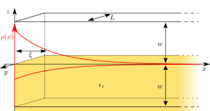
Placing this charge distribution on top of a substrate with relative permittivity induces a mirror charge , scaled by the factor . The electrostatic energy of the system is composed of two parts. The first component is given by the unscreened self interaction of the charge in the edge channel. It is reduced by the second component which models the screening of the dielectric through an interaction between the channel and . The electrostatic Coulomb energy therefore amounts to
| (S4) |
As the integral in Eq. (S4) cannot be solved analytically, we will focus on two tractable limiting cases. First, we assume , i. e. a negligible decay length. This reduces the dimensionality of the problem and results in the integral expression
| (S5) |
We can simplify the integrated expression by expanding in and find
| (S6) |
Second, we assume the perpendicular width of the channel to be negligible, , where Eq. (S4) reduces to
| (S7) |
Here, we can expand in and find
| (S8) |
where denotes Euler’s constant. Combining both limits from Eqs. (S6) and (S8) through a logarithmic interpolation yields
| (S9) |
This final result only deviates negligibly from a numerical evaluation of the full expression (S4). A theoretical estimate of in HgTe/CdTe QWs was performed in the work by Teo and Kane Teo and Kane (2009), who employ screening by a metallic gate in the vicinity of the edge channel and obtain a similar logarithmic interpolation formula. Using the experimental parameters and , they estimate the Luttinger parameter as , which indicates rather weak interactions. In contrast, we restrict ourselves to a dielectric screening by the SiC substrate, that keeps the long range character of the Coulomb interaction intact. The logarithmic divergence of the electrostatic energy of the edge channel in the limit of reflects the incomplete screening of the long-ranged Coulomb interaction. Our result is consistent with the observation that vanishes for infinitely long systems if metallic screening is neglected. Schulz (1994) Eq. (S9) is therefore only valid if is small compared to the distance between metallic gates and the edge channel. The explicit estimate for the bismuthene edge mode is obtained using , , as experimental parameters. By assuming a range of for the edge channel length and for the relative permittivity of the SiC substrate Patrick and Choyke (1970), we obtain a Luttinger parameter of . This places the 1D edge channel of bismuthene beyond the regime of weak interactions. It should be noted that for undoped SiC is an estimate in this simple modeling, as is known to increase for heavily doped semiconductors Dhar and Marshak (1985), which would result in enhanced screening. Notwithstanding further possible refinements of the current theoretical analysis, our approximation puts the theoretical prediction within the range of the Luttinger parameter extracted from STS scaling in experiment (see Tab. 1). Overall, the central parameter that governs the strong decrease in K from HgTe/CdTe QWs to bismuthene is the reduced channel width , which implies stronger Coulomb interactions induced by a substantially increased confinement of the quasi-1D DOS of the helical edge mode.
.3 STS spectra in close-up analysis
a) Logarithmic plot
b) Set-point variation
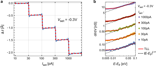
It is known that the electric field of the tunneling tip can induce band bending effects if the tunneling current is too high and the tip-to-sample distance becomes to small. We excluded possible tip induced effects on the power-law scaling of the ZBA by measuring spectra for different set-point voltages and currents ranging from and which apart from an overall scaling factor had no significant influence, see Fig. S4.
.4 Alternative Models for a Zero Bias Anomaly
The characteristic feature of a TLL is the power-law decay of the LDOS at low-energies. Moreover, spectra for different temperatures collapse onto an universal scaling curve as in Fig. 4 and S3. Yet, there are also alternative mechanisms that could potentially lead to a ZBA.
a) Efros-Schklovskii like Coulomb Pseudogap
In a low-dimensional metallic system the presence of disorder can lead to a suppression of spectral weight around zero energy. The phenomenon is an example for an Efros-Shklovskii like Coulomb pseudogap. The expected LDOS can be found to exhibit an exponential suppression according to Bartosch and Kopietz (2002)
| (S11) |
where depends on intrinsic properties of the system only, i.e., the electron-electron interaction and the diffusion coefficient , which reflects the strength of disorder in the system. The parameter will serve as a fitting parameter to our experimental data.
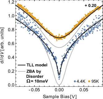
In contrast to the TLL model, however, the functional form of the arising ZBA in this scenario is described by an exponential decrease of the for low-energies. The functional form of the Coulomb pseudogap model according to Eq. (.4) with the interaction strength as the only free parameter is shown in Fig. S5. Whereas a coarse approximation to the data can be achieved for higher sample bias, only poor accordance is given for lower sample bias around . Particularly, matching of the exponential form according to Eq. (.4) with the data can not be achieved over the entire bias range of the ZBA. This evidences that a disorder induced Efros-Schklovskii-like Coulomb pseudogap cannot explain the observed spectral behavior.
b) Dynamical Coulomb Blockade
In case that the applied bias voltage is smaller than the resulting charging energy of the system, i.e., where is the total capacitance (described in the following), charging effects can in principle induce a ZBA in STS measurements. As an important example, one may consider an electrical circuit that contains an electromagnetic environment (e.g., the substrate) modeled by external impedances in the tunneling circuit. This type of models are usually referred to as dynamical Coulomb blockade (DCB) models.
In the framework of the DCB scenario, the STS tunneling experiment can conveniently be regarded as a double junction as in Fig. S6 Brun et al. (2012); Ming et al. (2018). Electrons tunnel from a metallic tip onto an ’island’ on the sample surface and subsequently into the substrate. Part of this double junction is a first tunneling junction (T-junction) which models the tunneling between tip and island with an effective capacitance in parallel with a resistance . The tunneling resistance can be inferred from the set-point current and voltage as , and is typically in our experiments. The tunneling capacitance is usually not known, but typically on the order of . Brun et al. (2012); Ming et al. (2018) The second junction which models a tunneling process of electrons from the sample surface into the substrate is a second -junction (S-junction) in series with the T-junction. The resistance and capacitance of the S-junction are usually unknown and form fit parameters in the DCB model.

The following model in terms of the DCB scenario is valid, if in an experimental STS measurement the complete bias voltage drops over the T-junction, i.e., , and as long as is comparable to the resistance quantum . Then tunneling in the DCB regime along with an excitation of the dissipative environment can be treated quantum mechanically by the so-called environment-quantum fluctuation or -theory Devoret et al. (1990), within which the tip to sample (sample to tip) tunneling probability () at temperature can be calculated as
| (S11a) | ||||
| (S11b) | ||||
where is the bias voltage, is the Fermi function and () are the energy levels at the tip (sample), respectively. and are the tip and sample LDOS, respectively. describes the probability that the electron looses the energy to the dissipative environment during the tunneling process. In the case of elastic tunneling where energy is conserved within the double junction during the tunneling event the probability factor reduces to a delta function .
In principle, the function can be calculated as Devoret et al. (1990):
| (S12) |
with
| (S13) |
where is the frequency dependent complex impedance as seen from the tunnel junction Brun et al. (2012). The frequency dependent complex impedance of the dissipative environment , on the other hand, depends solely on and of the S-junction. Consequently, the total impedance can be written as , with . The total tunneling current is calculated as the sum of the tunneling current in both directions .
In the following calculations, and are both taken to be constant in the bias range , which is reasonable since the tip has been ensured to be metallic and it has been seen that the bismuthene edge LDOS inside the bulk gap, despite the ZBA, is approximately constant. The functional form of the differential conductivity can be calculated as:
| (S14) |
In the case of and the -characteristic and the differential conductance become Devoret et al. (1990)
| (S15a) | ||||
| (S15b) | ||||
It is apparent that in this limit the is also characterized by a power-law (with a power-law exponent ), as is the case for tunneling into a TLL. This fact was pointed out by Safi et al. Safi and Saleur (2004).
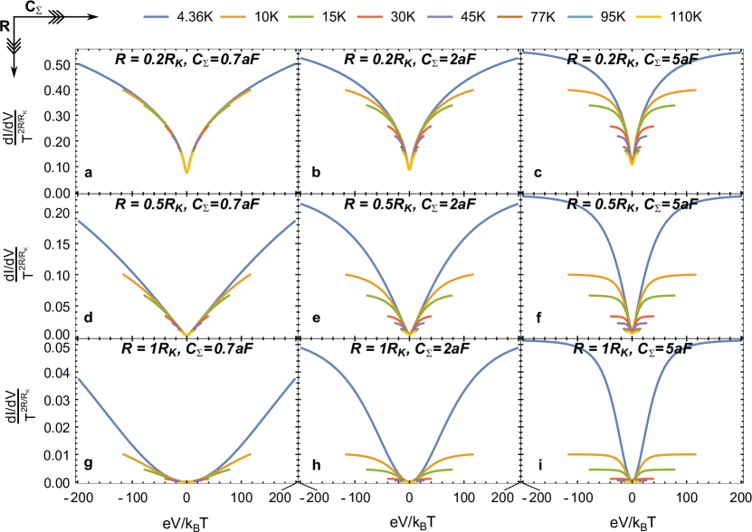
For arbitrary temperatures, however, it is not possible to give an analytic solution of the . One has to calculate it numerically by solving Eq. (S14). In Fig. S7 we present the result for different values of and and plot it on a rescaled conductivity and energy scale in order to detect coincidental universal scaling behavior in the bias voltage range (the voltage range where we observed the ZBA in bismuthene measurements). In the DCB model all ZBAs collapse onto a universal scaling curve only for parameters and and for spectra in the temperature range . In general, whereas mainly determines the depth and width of the ZBA, the main effect of is to determine the steepness of the ZBA.
We now want to discuss implications for our ZBA measurements that follow from the DCB model. First, we want to note that within the DCB model the metallic bismuthene edge channels form the capacitive island and are thought to have poor electrical contact to the SiC substrate modeled by the S-junction. A crude estimate is that bismuthene edge channels which cover a smaller area on the SiC substrate will affect the charging of the S-junction and consequently enlarge and reduce according to: and for a straight metallic edge with length and width (typically , see Fig. 1(c)). Therefore, and are local properties of the system Ming et al. (2018). Local deviations should therefore manifest in local differences of the power-law exponent and more importantly impede universal scaling. We measured the ZBA on four different samples and on various positions on each sample. The observation that we did not measure any significant deviations of the power-law exponent, not even for local variations of (), the size of the bismuthene domain nor variations of the set-point parameters and (Fig. S4), together with universal scaling (Fig. 4 and S3), strongly points towards the ZBA being a result of intrinsic properties of the 1D edge channel and hence the exclusion of the DCB scenario.
References
- Li et al. (2015) T. Li, P. Wang, H. Fu, L. Du, K. A. Schreiber, X. Mu, X. Liu, G. Sullivan, G. A. Csáthy, X. Lin, and R.-R. Du, Phys. Rev. Lett. 115, 136804 (2015).
- Väyrynen et al. (2016) J. I. Väyrynen, F. Geissler, and L. I. Glazman, Phys. Rev. B 93, 241301 (2016).
- Teo and Kane (2009) J. C. Y. Teo and C. L. Kane, Phys. Rev. B 79, 235321 (2009).
- Eggert (2000) S. Eggert, Phys. Rev. Lett. 84, 4413 (2000).
- Blumenstein et al. (2011) C. Blumenstein, J. Schäfer, S. Mietke, S. Meyer, A. Dollinger, M. Lochner, X. Y. Cui, L. Patthey, R. Matzdorf, and R. Claessen, Nat Phys 7, 776 (2011).
- Bockrath et al. (1999) M. Bockrath, D. H. Cobden, J. Lu, A. G. Rinzler, R. E. Smalley, L. Balents, and P. L. McEuen, Nature 397, 598 (1999).
- Calzona et al. (2015) A. Calzona, M. Carrega, G. Dolcetto, and M. Sassetti, Phys. Rev. B 92, 195414 (2015).
- Giamarchi (2003) T. Giamarchi, Quantum Physics in One Dimension, Clarendon Press Oxford (2003).
- Schulz (1994) H. J. Schulz, Mesoscopic Quantum Physics, Proceedings of the Les Houches Summer School, Session LXI, Elsevier Publishers (1994).
- Patrick and Choyke (1970) L. Patrick and W. J. Choyke, Phys. Rev. B 2, 2255 (1970).
- Dhar and Marshak (1985) S. Dhar and A. H. Marshak, Solid-state Electronics 28, 763 (1985).
- Bartosch and Kopietz (2002) L. Bartosch and P. Kopietz, The European Physical Journal B - Condensed Matter and Complex Systems 28, 29 (2002).
- Brun et al. (2012) C. Brun, K. H. Müller, I.-P. Hong, F. Patthey, C. Flindt, and W.-D. Schneider, Phys. Rev. Lett. 108, 126802 (2012).
- Ming et al. (2018) F. Ming, T. S. Smith, S. Johnston, P. C. Snijders, and H. H. Weitering, PRB 97, 075403 (2018).
- Devoret et al. (1990) M. H. Devoret, D. Esteve, H. Grabert, G.-L. Ingold, H. Pothier, and C. Urbina, Phys. Rev. Lett. 64, 1824 (1990).
- Safi and Saleur (2004) I. Safi and H. Saleur, Phys. Rev. Lett. 93, 126602 (2004).