Zero-bias Shapiro steps in asymmetric pinning nanolandscapes
Abstract
The coherent nonlinear dynamics of Abrikosov vortices in asymmetric pinning nanolandscapes is studied by theoretical modeling and combined microwave and dc electrical resistance measurements. The problem is considered on the basis of a single-vortex Langevin equation within the framework of a stochastic model of anisotropic pinning. When the distance over which Abrikosov vortices are driven during one half ac cycle coincides with one or a multiple of the nanostructure period, Shapiro steps appear in the current-voltage curves (CVCs) as a general feature of systems whose evolution in time can be described in terms of a particle moving in a periodic potential under combined dc and ac stimuli. While a dc voltage appears in response to the ac drive, the addition of a dc bias allows one to diminish the rectified voltage and eventually to change its sign when the extrinsic dc bias-induced asymmetry of the pinning potential starts to dominate the intrinsic one. This rectified negative voltage in the CVCs becomes apparent as zero-bias Shapiro steps, which are theoretically predicted and experimentally observed for the first time.
I Introduction
Periodic arrays of pinning sites are known to be effective for reducing the dissipation by Abrikosov vortices in type-II superconductors. In the presence of periodic pinning structures, the dynamics of vortices can be described as their motion in some periodic pinning potential Bra95rpp . In the most simple case such a potential is constant in one direction and periodic in the other, i. e. it is a pinning potential of the washboard type Dob17pcs . This type of pinning potential allows one to derive analytical expressions for the experimentally measurable quantities (dc voltage and absorbed ac power) for arbitrary values of the driving parameters (dc bias, ac amplitude and frequency) and temperature.
An intriguing effect in the vortex dynamics appears when the pinning potential is asymmetric Lee99nat ; Vil03sci ; Sil06nat ; Zap96prl ; Ust04prl ; Miz06jap . In this case the reflection symmetry of the pinning force is broken and thus, the depinning currents measured under current reversal are not equal. This is known as the ratchet effect, which in the context of the vortex dynamics is associated with systems Plo09tas where the vortex can acquire a motion whose direction is determined only by the pinning potential asymmetry with respect to the current direction reversal. In general, depending on the way to bring asymmetry into a system, one can distinguish between a fixed intrinsic asymmetry caused by the spatial asymmetry of the potential, and a tunable extrinsic asymmetry invoked by a dc bias. A vortex ratchet with internal pinning asymmetry is called a rocking ratchet, while a vortex ratchet with external pinning asymmetry is known as a tilted-potential or tilting ratchet. A tilting ratchet was theoretically considered in Shk11prb for a cosine washboard pinning potential (WPP) where its tilt is caused by a dc bias. In Ref. Shk11prb exact expressions for the experimentally accessible quantities (electrical voltage and absorbed ac power) were derived by using the matrix continued fractions technique Shk08prb . This method was recently extended Shk14pcm to an asymmetric potential of the washboard type. In this work, the theoretical results of Ref. Shk14pcm will be used for analysing the current-voltage curves (CVC) of superconductors with ratchet WPPs.
Another important effect consists in switching between the direct and the reversed net motion of the vortices and is termed the ratchet reversal effect Shk14pcm . This effect manifests itself as a sign change in the rectified voltage as a function of the driving force. Though a dozen of mechanisms for ratchet reversals are discussed in literature, as briefly outlined in the introductory part of Ref. Shk14pcm , one of the simplest mechanisms relies upon competition of the intrinsic and the extrinsic asymmetries of the pinning potential. It is this mechanism which will be discussed in this work for the vortex dynamics under combined dc and ac drives in a ratchet WPP.
On the experimental side, our previous work was concerned with investigations of the guided vortex motion in Nb films Dob12tsf with symmetric nanogrooves Dob12njp , the interplay of vortex guiding with the Hall effect Dob16sst and the dynamics of vortices at microwave frequencies Dob15mst ; Dob15snm ; Dob15apl ; Dob15met ; Sil17inb . On the one hand, Shapiro steps were revealed in the CVCs of Nb films with periodically arranged symmetric nanogrooves Dob15mst ; Dob15snm . That provided evidence that when the location of vortices geometrically matches the location of the pinning sites, the vortex dynamics is coherent, so that the dynamics of the whole vortex ensemble can be analyzed in terms of the single-vortex dynamics Luq07prb . In general, Shapiro steps appear in the current-voltage curves (CVCs) as a general feature of systems whose evolution in time can be described in terms of a particle moving in a periodic potential under combined dc and ac stimuli. The observation of Shapiro Sha63prl steps in different systems dates back to the works of Fiory Fio71prl ; Fio73prb , Martinoli Mar75ssc ; Mar76prl and others Day67prv ; Ben90prl ; Loo99prb ; Mat09prb ; Siv03prl ; Naw13prl ; Rei00prb ; Rei15prbS .
On the other hand, the dc current polarity has been revealed to be crucial for the reduction of the so-called depinning frequency Git66prl ; Cof91prl ; Pom08prb ; Sil17inb in Nb films with asymmetric grooves, thus allowing for the design of microwave cutoff filters Dob15apl and fluxonic metamaterials Dob15met . In addition, an analysis of experimental data on the microwave power absorption using the approach outlined in Refs. Shk08mmt ; Shk12inb ; Shk13ltp has allowed us to deduce the coordinate dependences of the pinning potentials in these samples Dob15vor . Since the deduced coordinate dependences turned out asymmetric Dob15vor , this motivated us to theoretically analyze the CVCs for the films with asymmetric WPPs and to examine the predicted effects experimentally.
Here, we theoretically analyze the appearance of zero-bias Shapiro steps in the CVCs of superconductors with asymmetric washboard pinning landscapes as functions of the asymmetry strength parameter and the ac amplitude. On the experimental side, studying the voltage response by combined microwave ( MHz – GHz) and dc electrical resistance measurements, we reveal the theoretically predicted zero-bias Shapiro steps which are absent in the CVCs of superconducting films with symmetric WPPs. These zero-bias Shapiro steps originate from the negative ratchet effect which is caused by the different groove slopes’ steepnesses in the studied Nb films.
II Theoretical model
The geometry of the problem is sketched in Fig. 1. Its theoretical treatment relies upon the Langevin equation for a vortex moving with velocity in a magnetic field , where , , is the unit vector in the direction and , which in neglect of the Hall effect reads Shk08prb
| (1) |
where is the Lorentz force, is the magnetic flux quantum, and is the speed of light. In Eq. (1) , where and are the dc and ac current density amplitudes and is the angular frequency. is the anisotropic pinning force, where is a ratchet WPP. is the thermal fluctuation force represented by Gaussian white noise and is the vortex viscosity.
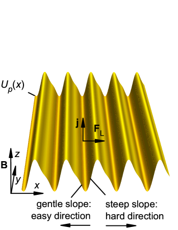
The ratchet WPP is modeled by
| (2) |
where . Here is the period and is the depth of the WPP. In Eq. (2) is the asymmetry parameter allowing for tuning the asymmetry strength. In particular, Eq. (2) yields a symmetric WPP when and a double-well WPP when , refer to the inset of Fig. 2. In what follows, we will focus on the case , as representative for the most commonly Bar94epl ; Han96inc ; Zap96prl ; Mat00prl ; Pop00prl ; Zar09pre ; Arz11prl used ratchet potential. Evidently, the left and right barriers of the ratchet WPP have different steepnesses. For definiteness, the positive current polarity corresponds to the vortex motion in the positive direction of the -axis direction against the steep slope of the WPP in Fig. 1.
The Langevin equation (1) can be solved in terms of the matrix continued fractions Shk14pcm . For this one introduces dimensionless parameters, namely, the dc density and the ac density amplitude . Here and is the depinning current density corresponding to the WPP barrier vanishment. Further dimensionless parameters are the frequency , where is the depinning frequency with being the relaxation time for the vortex, the coordinate and the inverse temperature . The experimentally deducible quantities are the microwave power absorbed by vortices and the dc electric field strength. It is the dc electric field strength on which we focus in this work. Namely, in units of the flux-flow resistivity, , the time-independent average dc electric field reads Shk14pcm
| (3) |
Here is the -dependent effective nonlinear mobility of the vortex under the influence of the dimensionless generalized moving force in the direction and it is expressed in terms of the matrix continued fractions Shk14pcm .
In what follows we discuss the modification of the CVCs calculated by Eq. (3) for a series of values of the asymmetry parameter and the ac amplitude at the reduced temperature . Note, this corresponds to the experimental situation, e. g. Nb thin films with nanogrooves, where the pinning activation energy is of the order of K Dob12njp and the measurements are conducted in the vicinity of the superconducting transition temperature K. The computing procedure with the matrix continued fractions is detailed in Ref. Shk14pcm .
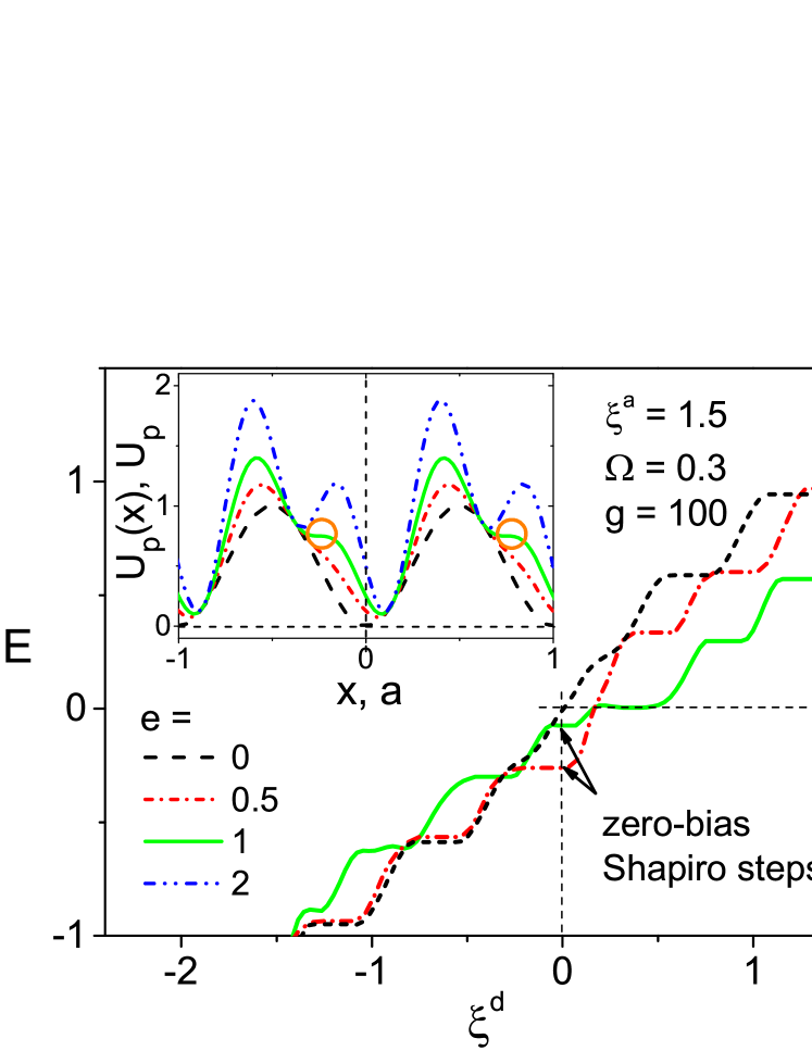
Figure 2 presents the CVCs calculated for a series of at the frequency and the overcritical ac amplitude . The meaning of the critical amplitude is explained in Fig. 4. In Fig. 3 all CVCs demonstrate Shapiro-like steps regardless of the associated value. This synchronization effect is generic to systems with a periodic potential subjected to combined dc and ac stimuli. The presence of steps in the CVC for a cosine WPP was reported in Shk08prb referring back to an analysis Van85prb of the overall shape and positions of steps in the Josephson junction problem, as observed first by Shapiro Sha63prl . In contrast to the cosine potential for in Fig. 2, several new features appear in the CVCs thanks to the asymmetry of the WPP. First, whereas the regime of viscous flux flow is realized for over the entire range of dc biases, the CVC for has a zero plateau on the right-hand branch as long as the critical dc bias for the steep-slope direction of the WPP is not reached. Second, due to the asymmetry of the WPP, the positive (steep-slope) critical current value is greater than the negative (gentle-slope) one . Since , the threshold in the left branch of the CVC is absent. Finally, the curves for and demonstrate a negative voltage at small positive biases. This is a clear indication for the ratchet reversal effect, which is most pronounced at .
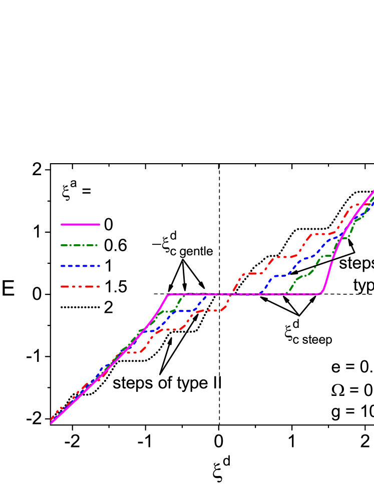
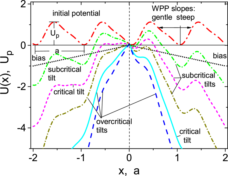
Turning to the influence of the ac amplitude on the shape of the CVCs shown in Fig. 3, the curve for should be discussed first. This curve has two unequal-arm branches each having a zero plateau as long as the corresponding critical tilt of the WPP is not reached. In the limit of very strong dc biases the curve tends to the Ohmic behavior whose slope is determined by the flux-flow resistivity . If one defines the critical dc bias as that corresponding to the vanishing WPP barrier in Fig. 4, then it is evident that for the gentle-slope (left) WPP barrier the critical dc density is less than for the steep-slope (right) WPP barrier. This feature allows for the rectification of ac signals (the diode effect), provided the ac amplitude satisfies the condition .
With increasing ac amplitude several changes in the CVC in Fig. 3 should be emphasized. First, for both branches the absolute value of the dc critical density is reduced. Accordingly, is a decreasing function of the ac drive. The physical reason for this lies in the replacement of the dc critical density by the total (dc+ac) critical amplitude with one additional contribution originating from the asymmetry parameter . This contribution is negative for the steep-slope direction and it is positive for the gentle-slope one Shk14pcm .
The second feature is the development of Shapiro-like steps in the CVCs with increasing . Depending on the relative strength of the ac current amplitude with respect to its critical value , two different types of steps in the CVC ensue. The steps of type I appear at (overcritical ac amplitudes) and distort the CVC like a ripple with a downward shift from the Ohmic line. The stronger the broader is the range of for these steps to appear. The steps of type II ensue for (subcritical ac amplitudes) and oscillate closely around the Ohmic line. With increasing the size of the steps of both types increases, whereas their number decreases. In the opposite limiting case of very low frequencies , i. e. in the quasistatic regime, all steps reduce their size along with increasing their number. All steps saturate to the conventional smooth CVC with decreasing ac amplitude.
The third feature consists in the appearance of a negative voltage at small positive dc biases. This ratchet reversal ensues for overcritical ac amplitudes with respect to both, the gentle-slope and the steep-slope WPP barriers. The physical reason for the negative voltage to appear is the rectifying effect due to the internal anisotropy of the WPP. An increase of the dc bias superimposes the external tilt-induced asymmetry onto the original intrinsic asymmetry of the WPP, see Fig. 4. This is why the direct net transport starts to prevail over the reversed one.
An examination of the main theoretical predictions for superconducting Nb thin films with an asymmetric washboard pinning nanostructure is reported next.
III Experiment
The sample is a nm-thick epitaxial Nb (110) film prepared by dc magnetron sputtering onto an a-cut () sapphire substrate Dob12tsf . The film was pre-patterned by standard photolithography followed by Ar ion-beam etching in order to define a impedance-matched microstrip with a width of m and a length of m. A washboard pinning nanolandscape was then fabricated on the microstrip surface by focused ion beam (FIB) milling. The nanopattern is an array of uniaxial straight grooves with a groove-to-groove distance of nm, a depth of nm, and a full width at half depth of nm. The grooves are aligned parallel to the long side of the microstrip, that is parallel to the transport current direction. They have an asymmetric profile in the cross-section that has been achieved in the patterning process by defining a step-wise increasing number of FIB beam passes to each groove screened as a 5-step “staircase”. In Fig. 5, one sees that due to blurring effects, smooth slopes resulted instead of the “stairs” in the nanopattern. It is worth noting that the microstrip width is an integer multiple number () of the nanopattern period and the accuracy of FIB milling in conjunction with the large microstrip dimensions ensure that possible ratchet effects due to the edge barrier asymmetry Ali09njp are insignificant to the highest attainable degree. The film is characterized by a critical temperature of K and by an upper critical field at zero temperature of about T, as deduced from fitting the dependence to the phenomenological law .
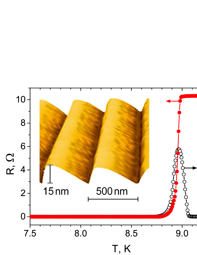
Combined microwave and dc electrical resistance measurements were done with magnetic field directed perpendicular to the film surface, using a custom-made sample probe equipped with coaxial cables Dob15mst . The microwave signal was generated by an Agilent E5071C vector network analyzer, while the dc signal was added by using two bias-tees mounted at the ports of the analyzer. The CVCs were measured in the fixed-current upsweep mode Dob15apl ; Dob15met . The complementary measurements of the microwave power absorbed by vortices Dob15apl ; Dob15met allowed us to deduce the coordinate dependence of the mean pinning potential in a series of samples with different grooves’ asymmetry degrees, using the procedure outlined in Shk12inb ; Shk13ltp . Accordingly, for the sample used in this work the coordinate dependence of the pinning potential has been approximated by Eq. (2) with which is very close to used for the simulation results presented in Sec. II.
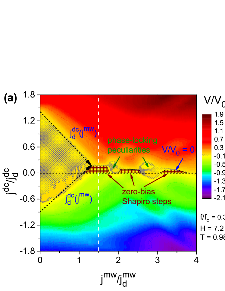
Figure 6 displays the dc electrical voltage as a function of the normalized dc density and the ac amplitude for the ac frequency MHz. The measurements are done at the temperature and the fundamental matching field mT. The arrangement of vortices at mT with respect to the pinning nanolandscape is shown in the inset of Fig. 6(b) for the assumed triangular vortex lattice with lattice parameter and the matching condition . In the absence of microwave excitation, the CVC in Fig. 6(b) demonstrates two different absolute values of the depinning current density for the positive and the negative branch. The depinning current density is determined by the V voltage criterion, while we use the mean-square parameter for the presentation of the data in dimensionless form allowing for a direct comparison of experiment with theory. At and mT the depinning current densities for the gentle-slope and the strong-slope directions of the nanostructure amount to MA/cm2 and MA/cm2, respectively. Accordingly, this yields the mean-square depinning current mA.
The addition of the microwave stimulus leads to the appearance of Shapiro steps in the CVC. The steps occur at voltages Fio71prl
| (4) |
where is an integer, is the number of vortex rows between the voltage leads, is the microwave frequency, and Vs is the magnetic flux quantum. The steps in the CVCs arise when one or a multiple of the hopping period of Abrikosov vortices coincides with the period of the ac drive. One can distinguish up to five lowest-order Shapiro steps and from the step voltage one can infer -. This is similar to the Nb films with symmetric grooves dealt with previously Dob15snm . Given the geometrical dimensions of the microstrip and the fundamental matching field configuration for a triangular vortex lattice [see the inset to Fig. 6(b)], the expected number of vortex rows between the voltage leads is equal to . The fact that the number of vortex rows deduced from fitting the experimental data to Eq. (4) is very close to suggests that all vortices move coherently. This strongly coherent motion is caused by both, the high periodicity of the nanogroove array and a relatively weak contribution of the background isotropic pinning due to structural imperfectness as compared to the dominating strong pinning owing to the nanopatterning. This conclusion is in line with our previous observations Dob12njp ; Dob15snm that the focused ion beam-milled grooves provide a strong pinning potential for vortices forced to move across them. When tuning the field value away from the matching configuration the steps disappear.
Turning to the general description of the contour plot in Fig. 6(a), several features should be noted. First, the dc depinning current value nearly linearly decreases with increasing microwave amplitude, i. e. the experimental data confirm the theoretical prediction that the microwave current density contributes to the depinning of vortices. Second, at the dc depinning values turn out to be zero and this leads to the effective “symmetrization” of the CVC, but with the origin shifted by towards the positive bias values. The theory suggests that at this dc bias the internal asymmetry of the pinning potential is effectively compensated by the extrinsic asymmetry of the WPP caused by the dc bias. This allows one to interpret this dc value as that characterizing the loading capability of the ratchet Knu12pre . Third, at relatively small positive dc values for the microwave amplitudes a small negative voltage is revealed. With further increasing dc value the voltage tends to zero and changes its sign, that is the ratchet reversal is observed. Finally, at some microwave amplitudes an enhancement of the dc voltage is observed, as designated by “phase-locking peculiarities” in Fig. 6(a). Similar peculiarities were theoretically predicted earlier for a symmetric Shk11prb and an asymmetric Shk14pcm WPPs so that we believe that the features observed experimentally correspond to the three lowest-order mode-locking fringes discussed in Shk14pcm .
IV Conclusion
In the presence of combined dc and microwave drives the vortex dynamics in asymmetric pinning potentials exhibits several dynamical regimes which are determined not only by the magnitude of the applied current, but also by its polarity. These different regimes in the vortex dynamics have been analyzed in the framework of a stochastic single-vortex model on the basis of the Langevin equation. This allows for a direct comparison of the coherent vortex dynamics of the vortex ensemble in Nb films with asymmetric grooves at the fundamental matching field with the theoretical predictions derived in the single-vortex approach. This early experiment has revealed the main features of the current-voltage curves predicted theoretically, namely:
-
•
The CVC of a superconductor with an asymmetric WPP is characterized by two different depinning current values in the positive and the negative branch.
-
•
The dc depinning current density values for both dc polarities decrease linearly with increasing microwave amplitude. The microwave amplitude corresponding to the intersection of the -dependences for both dc polarities allows one to infer the dc value at which the internal asymmetry of the pinning potential is compensated by its external asymmetry induced by the tilt due to the dc bias.
-
•
A switching between the positive and the negative ratchet effect (ratchet reversal) takes place depending on the balance between the fixed internal and the dc-bias tunable asymmetry of the pinning potential.
-
•
A negative voltage at zero dc bias becomes apparent as zero-bias Shapiro steps which can be explained as a synchronization effect in the current-voltage curve shifted from its origin due to the asymmetry of the pinning potential.
This work was financially supported by the German Research Foundation (DFG) through grant DO 1511 and conducted within the framework of the NanoSC-COST Action MP1201 of the European Cooperation in Science and Technology. This research has received funding from the European Union s Horizon 2020 research and innovation program under Marie Sklodowska-Curie Grant Agreement No. 644348 (MagIC).
References
- (1) E. H. Brandt, Rep. Progr. Phys. 58 (1995) 1465–1594.
- (2) O. V. Dobrovolskiy, Physica C 533 (2017) 80–90.
- (3) C.-S. Lee, B. Janko, I. Derenyi, A.-L. Barabasi, Nature 400 (1999) 337–340.
- (4) J. E. Villegas, S. Savel’ev, F. Nori, E. M. Gonzalez, J. V. Anguita, R. Garcia, J. L. Vicent, Science 302 (2003) 1188–1191.
- (5) C. C. de Souza Silva, J. Van de Vondel, M. Morelle, V. V. Moshchalkov, Nature 440 (2006) 651–654.
- (6) I. Zapata, R. Bartussek, F. Sols, P. Hänggi, Phys. Rev. Lett. 77 (1996) 2292–2295.
- (7) A. V. Ustinov, C. Coqui, A. Kemp, Y. Zolotaryuk, M. Salerno, Phys. Rev. Lett. 93 (2004) 087001.
- (8) Y. Mizugaki, K. Katoh, J. Appl. Phys. 100.
- (9) B. L. T. Plourde, IEEE Trans. Appl. Supercond. 19 (2009) 3698–3714.
- (10) V. A. Shklovskij, O. V. Dobrovolskiy, Phys. Rev. B 84 (2011) 054515–1–12.
- (11) V. A. Shklovskij, O. V. Dobrovolskiy, Phys. Rev. B 78 (2008) 104526–1–12.
- (12) V. A. Shklovskij, V. V. Sosedkin, O. V. Dobrovolskiy, J. Phys.: Cond. Matt. 26 (2014) 025703.
- (13) O. V. Dobrovolskiy, M. Huth, Thin Solid Films 520 (2012) 5985–5990.
- (14) O. V. Dobrovolskiy, E. Begun, M. Huth, V. A. Shklovskij, New J. Phys. 14 (2012) 113027–1–27.
- (15) O. V. Dobrovolskiy, M. Hanefeld, M. Zörb, M. Huth, V. A. Shklovskij, Superond. Sci. Technol. 29 (2016) 065009–1–7.
- (16) O. V. Dobrovolskiy, J. Franke, M. Huth, Meas. Sci. Technol. 26 (2015) 035502.
- (17) O. V. Dobrovolskiy, J. Supercond. Nov. Magnet. 28 (2015) 469–473.
- (18) O. V. Dobrovolskiy, M. Huth, Appl. Phys. Lett. 106 (2015) 142601–1–5.
- (19) O. V. Dobrovolskiy, M. Huth, V. A. Shklovskij, Appl. Phys. Lett. 107 (2015) 162603–1–5.
- (20) E. Silva, N. Pompeo, O. V. Dobrovolskiy, Vortices at microwave frequencies, Walter De Gruyter Inc., Berlin, 2017, Ch. 8.
- (21) Q. Lu, C. J. O. Reichhardt, C. Reichhardt, Phys. Rev. B 75 (2007) 054502.
- (22) S. Shapiro, Phys. Rev. Lett. 11 (1963) 80–82.
- (23) A. T. Fiory, Phys. Rev. Lett. 27 (1971) 501–503.
- (24) A. T. Fiory, Phys. Rev. B 7 (1973) 1881–1889.
- (25) P. Martinoli, O. Daldini, C. Leemann, E. Stocker, Solid State Commun. 17 (1975) 205–209.
- (26) P. Martinoli, O. Daldini, C. Leemann, B. Van den Brandt, Phys. Rev. Lett. 36 (1976) 382–385.
- (27) A. H. Dayem, J. J. Wiegand, Phys. Rev. 155 (1967) 419–428.
- (28) S. P. Benz, M. S. Rzchowski, M. Tinkham, C. J. Lobb, Phys. Rev. Lett. 64 (1990) 693–696.
- (29) L. Van Look, E. Rosseel, M. J. Van Bael, K. Temst, V. V. Moshchalkov, Y. Bruynseraede, Phys. Rev. B 60 (1999) R6998–R7000.
- (30) T. Matsuura, K. Inagaki, S. Tanda, Phys. Rev. B 79 (2009) 014304.
- (31) A. G. Sivakov, A. M. Glukhov, A. N. Omelyanchouk, Y. Koval, P. Müller, A. V. Ustinov, Phys. Rev. Lett. 91 (2003) 267001–1–4.
- (32) S. Nawaz, R. Arpaia, F. Lombardi, T. Bauch, Phys. Rev. Lett. 110 (2013) 167004.
- (33) C. Reichhardt, R. T. Scalettar, G. T. Zim’anyi, N. Gronbech-Jensen, Phys. Rev. B 61 (2000) R11914–R11917.
- (34) C. Reichhardt, C. J. O. Reichhardt, Phys. Rev. B 92 (2015) 224432.
- (35) J. I. Gittleman, B. Rosenblum, Phys. Rev. Lett. 16 (1966) 734–736.
- (36) M. W. Coffey, J. R. Clem, Phys. Rev. Lett. 67 (1991) 386–389.
- (37) N. Pompeo, E. Silva, Phys. Rev. B 78 (2008) 094503–1–10.
- (38) V. A. Shklovskij, Determination of coordinate dependence of the washboard pinning potential from the dynamic experiment with vortices, in: Procedings of the Fifth International Conference on Mathematical Modeling and Computer Simulation of Materials Technologies MMT-2008, Ariel, Israel, 2008.
- (39) V. A. Shklovskij, O. V. Dobrovolskiy, Microwave Absorption by Vortices in Superconductors with a Washboard Pinning Potential, InTech, Rijeka, 2012, Ch. 11, pp. 263–288.
- (40) V. A. Shklovskij, O. V. Dobrovolskiy, Low Temp. Phys. 39 (2013) 120–124.
- (41) a. O.? V.? Dobrovolskiy, ? M.? Huth, Assessment of periodic pinning in? superconductors? at? microwaves, in: Abstract book of the Ninth International? Conference? on? Vortex? Matter? in? Nanostructured Superconductors, Rhodes? (Greece)? , 12-17? September,? 2015? .
- (42) R. Bartussek, P. Hänggi, J. G. Kissner, Europhys. Lett. 28 (1994) 459.
-
(43)
P. Hänggi, R. Bartussek, Brownian
rectifiers: How to convert brownian motion into directed transport, in:
J. Parisi, S. Müller, W. Zimmermann (Eds.), Nonlinear Physics of Complex
Systems, Vol. 476 of Lecture Notes in Physics, Springer, Berlin Heidelberg,
1996, pp. 294–308.
URL http://dx.doi.org/10.1007/BFb0105447 - (44) J. L. Mateos, Phys. Rev. Lett. 84 (2000) 258–261.
- (45) M. N. Popescu, C. M. Arizmendi, A. L. Salas-Brito, F. Family, Phys. Rev. Lett. 85 (2000) 3321–3324.
- (46) D. G. Zarlenga, H. A. Larrondo, C. M. Arizmendi, F. Family, Phys. Rev. E 80 (2009) 011127.
- (47) A. V. Arzola, K. Volke-Sepúlveda, J. L. Mateos, Phys. Rev. Lett. 106 (2011) 168104.
- (48) C. Vanneste, C. C. Chi, K. H. Brown, A. C. Callegari, M. M. Chen, J. H. Greiner, H. C. Jones, K. K. Kim, A. W. Kleinsasser, H. A. Notarys, G. Proto, R. H. Wang, T. Yogi, Phys. Rev. B 31 (1985) 4230–4233.
- (49) F. G. Aliev, A. P. Levanyuk, R. Villar, J. F. Sierra, V. V. Pryadun, A. Awad, V. V. Moshchalkov, New J. Phys. 11 (2009) 063033.
- (50) M. Knufinke, K. Ilin, M. Siegel, D. Koelle, R. Kleiner, E. Goldobin, Phys. Rev. E 85 (2012) 011122–1–9.