Layered semiconductor EuTe4 with charge density wave order in square tellurium sheets
Abstract
We report a novel quasi-two dimensional compound of EuTe4 hosting charge density waves (CDW) instability. The compound has a crystallographic structure in a orthorhombic space group Pmmn (No.59) with cell parameters a = 4.6347(2)Å, b = 4.5119(2)Å, c = 15.6747(10)Å at room temperature. The pristine structure contains consecutive near-square Te sheets separated by corrugated Eu-Te slabs. Upon cooling, the compound experiences a phase transition near 255 K. X-ray crystallographic analysis and transmission electron microscopy (TEM) measurements reveal strong structural distortions in the low temperature phase, showing a 1a 3b 2c superstructure with a periodic formation of Te-trimers in the monolayer Te sheets, yielding evidence for the formation of CDW order. The charge transport properties show a semiconducting behavior in the CDW state. Density functional theory calculations reveals a Fermi surface nesting driven instability with a nesting vector in good agreement with the one observed experimentally. Our finding provides a promising system for the study of CDW driven 2D semiconducting mechanisms, which would shed a new light on exploring novel 2D semiconductors with collective electronic states.
pacs:
I Introduction
Charge density waves (CDWs) are collective electronic condensate arising from strong coupling of conduction electrons and the underlying lattice in low-dimensional metals Grüner (1988); Monceau (2012); Ajisaka et al. (2009). The subject has generated considerable interest in condensed matter physics due to its important insight into electron-phonon interaction and its potential role in the phase diagram of superconducting cuprates Wu et al. (2011); Kawasaki et al. (2017); Chang et al. (2012). Most CDW formations are driven by Fermi surface (FS) nesting effect, i.e., the matching of sections of FS to others by a wave vector q, which is favorable to lower the electronic energy of a system. In quasi-1D CDW systems, the perfect nesting condition can be easily realized and the FS would be fully gapped, resulting in a semiconducting or insulating phase, as manifested in most quasi-1D materials. While for higher dimensional systems, the FS nesting could hardly remove all parts of the FSs. In this circumstance, the CDW energy gap opens up only at the nested parts of FSs. Due to the residual ungapped regions of FSs, the CDW phase tends to keep metallic. Though a few examples exhibit semiconducting 2D CDW states, their semiconducting property is not truly driven by the FS nesting but by Mott interaction Colonna et al. (2005); Sipos et al. (2008) or by other physical mechanisms Kidd et al. (2002); Li et al. (2007).
The quasi-2D binary rare-earth pollytellurides RTen (where R is a lanthanide, n=2, 2.5, 3) are well-known systems with FS nesting-driven CDW states Malliakas et al. (2008); Hu et al. (2014); Gweon et al. (1998); Brouet et al. (2004); Patschke and Kanatzidis (2002); Papoian and Hoffmann (2000); Malliakas et al. (2005); Schmitt et al. (2008); Kim et al. (2006). The common structure of these compounds contain consecutive square Te sheets separated by isolated corrugated R-Te slabs. is normally trivalent in the compound, donating three electrons to the system. They completely fill the Te p orbitals in the R-Te slabs, but partially fill those Te p orbitals in the planar Te sheets. In their CDW state, these compounds remain metallic because of the imperfect FS nesting. Among RTen series, LaTe2 has been suggested to be a potential instance having semiconducting CDW state. However, the reported charge transport properties indicate that LaTe2 is a bad-metal rather than an insulator Min et al. (2002); Shin et al. (2005); Kwon and Min (2000). The detailed infrared spectroscopy studies on LaTe2 are also not consistent with the entirely gapped FS in its CDW stateHuang et al. (2012); Lavagnini et al. (2007).
Here we report a novel compound of quasi-2D divalent rare-earth telluride EuTe4 which exhibits a striking semiconducting behavior in CDW state. The prime structure of this compound can be considered as derived from the LaTe2-type structure by intercalating two more Te atomic sheets between the doublet Eu-Te corrugated slabs. Upon cooling, the x-ray crystallographic analysis and transmission electron microscopy (TEM) study reveal strong in-plane structural distortions, with a 1a 3b superstructure modulation, yielding evidence for the formation of CDW order. The temperature-dependent charge transport measurements confirm the transition occurring around temperature Tc = 255 K. After the transition, the state exhibits a narrow-gap semiconducting behavior, with the activation energy gap estimated to be 25 meV by the Arrhenius law. This semiconducting phase is further analyzed based on the Density Functional Theory (DFT) calculations. The modeling indicates that the FS topology favors a nesting vector along the b-axis direction with a value of q = b∗/3 (where b∗ = 2/b), which is quite well consistent with the experimental observations. Our result suggests a nesting driven CDW phase in EuTe4, which lowers the electronic energy of the system and is responsible for the semiconducting properties.
II Results and discussion
EuTe4 single crystals were grown via the Te flux approach. High-purity Eu lumps (99.999%) and Te granules (99.999%) were mixed with a ratio of 1 : 15. The total weighted starting materials were sealed in an evacuated fused silica tube in high vacuum (10-5 mbar) followed by heating at 850 ∘C for 2 days in a muffle furnace. Then the furnace was slowly cooled to 415 ∘C in 100 hours, and hold at this temperature for one weak then decanted using a centrifuge. The crystals are planar shaped with dark and mirror-like surfaces.
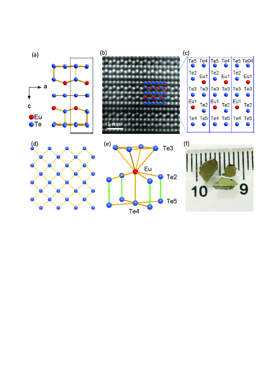
The crystallographic structure analysis of EuTe4 single crystals gives a symmetry of Pmmn (No.59) with cell parameters a = 4.5119(2)Å, b = 4.6347(2)Å, c = 15.6747(10) Å near room temperature (RT), as shown in Figure 1a. The structure can be considered as derived from the LaTe2-type structure by intercalating two more Te atomic sheets into the doublet Eu-Te slabs (Figure S1). The quantitative energy dispersive X-Ray spectroscopy (EDX) analysis of the compounds (Figure S2) gives the atomic ratio of Eu:Te close to a stoichiometric 1:4, consistent with the crystal refinement results (Table 1). Figure 1b is an atomic-resolution high angle annular dark field (HAADF) scanning transmission electron microscope (STEM) image of EuTe4, highlighting the structure of quintuple layer stacking. Between the adjacent quintuple layers, the nearest bond (Te-Te) is 3.37 Å, which is much larger than the normal covalent Te-Te bond of 2.8 Å, indicating weak inter-layer interactions.
A striking structural feature of EuTe4 is the appearance of the regular near-square nets made of the monolayer Te atoms. Figure 1c depicts the four different crystallographic positions of Te atoms, verifying two inequivalent Te sheets of Te(3) and Te(4)-Te(5) networks. Within these Te sheets (Figure 1d), the Te-Te bonding is 3.2341(1) Å- a typical hypervalent Te-Te bond lengthPapoian and Hoffmann (2000), suggesting high propensity for structural distortions. In the title compound, the Eu atom is 9-coordinate in an square antiprismatic geometry, as shown in Figure 1e. The near-neighbouring Eu-Te bond length, having the value between 3.3125(6)Å (Eu-Te(2) ) and 3.517(2) Å(Eu-Te(3)), are compatible with the global -Te distances observed in Ten families. Figure 1f shows the photograph of typical single crystals.
| Empirical formula | EuTe4 |
|---|---|
| Formula weight | 662.36 |
| Temperature | 289.98(11) K |
| Crystal system | orthorhombic |
| Space group | Pmmn |
| unit cell dimens | a = 4.5119(2)Å, = 90∘ |
| b = 4.6347(2)Å, = 90∘ | |
| c = 15.6747(10)Å, = 90∘ | |
| Volume, Z | 327.78(3) Å3, 2 |
| density(calcd) | 6.711 g/cm3 |
| absorp coeff | 26.872 mm-1 |
| F(000) | 542.0 |
| Crystal size ( mm3 ) | 0.15 0.1 0.02 |
| Radiation | Mok ( = 0.71073Å) |
| 2 range for data collection | 5.198∘ to 52.732∘ |
| Index ranges | -5 h 5, -3 k 5, -19 l 19 |
| Reflections collected | 2880 |
| Independent reflections | 429 [ Rint = 0.0481, Rsigma = 0.0286 ] |
| Data/restraints/parameters | 429/0/21 |
| Goodness-of-fit on F2 | 1.095 |
| Final R indexes [I =2 (I)] | R1 = 0.0456, wR2 = 0.1340 |
| Final R indexes [all data] | R1 = 0.0468, wR2 = 0.1347 |
| Largest diff. peak/hole / e ( Å3 ) | 4.28/-3.60 |
| Empirical formula | Eu3Te12 |
|---|---|
| Formula weight | 1987.08 |
| Temperature | 81(2) K |
| Crystal system | orthorhombic |
| Space group | P21cn |
| unit cell dimens | a = 4.4898(3)Å, = 90∘ |
| b = 13.8903(11)Å, = 90∘ | |
| c = 31.268(2)Å, = 90∘ | |
| Volume, Z | 1950.0(2) Å3, 4 |
| density(calcd) | 6.768 g/cm3 |
| absorp coeff | 27.101 mm-1 |
| F(000) | 3252.0 |
| Crystal size ( mm3 ) | 0.272 0.097 0.094 |
| Radiation | Mok ( = 0.71073Å) |
| 2 range for data collection | 3.922∘ to 52.738∘ |
| Index ranges | -5 h 5, -17 k 17, -39 l 39 |
| Reflections collected | 18379 |
| Independent reflections | 3908 [ Rint = 0.0660, Rsigma = 0.0530 ] |
| Data/restraints/parameters | 3908/85/131 |
| Goodness-of-fit on F2 | 1.073 |
| Final R indexes [I =2 (I)] | R1 = 0.0707, wR2 = 0.1953 |
| Final R indexes [all data] | R1 = 0.0827, wR2 = 0.2032 |
| Largest diff. peak/hole / e ( Å3 ) | 4.38/-4.41 |
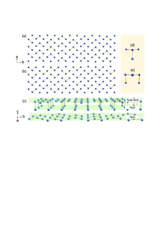
Hinted by the binary rare-earth polytellurides RTen (n=2, 2.5, 3), the presence of square Te sheets in the structure suggests that the compound is susceptible to Peierls instability, as the distorted structure is more energetically stable than the ideal square net structureTremel and Hoffmann (1987); Papoian and Hoffmann (2000). To reveal further characteristics of the structural distortions, the low temperature single-crystal X-ray diffraction analysis was employed. The result indicates that the system evolves into a modulated structural phase at cooling temperatures, showing a new structural symmetry Pna21 (Table 2). An in-plane commensurate supercell 1a 3b is constructed. Figure 2a and 2b depict such the fragments of the modulated structures of the Te sheets projected onto the ab plane at 81K. The modulated pattern can be seen as a sequence of V-shaped trimers in the planar Te nets. This converts a situation of all weak bonding in the undistorted monolayer Te sheets to a situation of some strong and some weak bondings in the distorted Te sheets. For instance, Te(3) monolayer sheets (Figure 2a), the minimum, maximum and average Te-Te distance after the distortion are 3.0064(4) Å, 3.4701(4) Å and 3.1824(7) Å, respectively. The similar distortions also exist in Te(4)-Te(5) networks (Figure 2b),with the minimum, maximum and average Te-Te distance of 2.8364(4) Å, 3.4919(5) Å and 3.2650(1) Å, respectively. Corresponding to the displacement distortions in the Te sheets, the in plane Te-Te bond angle are strongly deformed as well. For those Te-trimers, the bond angle is 99.89∘ in Te(3) sheets and 100.585∘ in Te(4)-Te(5) sheets, showing strong deviations from the right angle. In the distorted structure, the Te-trimers in Te(4)-Te(5) sheets combine with Te(2) atoms through the covalent Te-bonds give rise to the 3D structural formations of Te tetramers and pentamers, as displayed in Fig. 2c, 2d, and 2e.
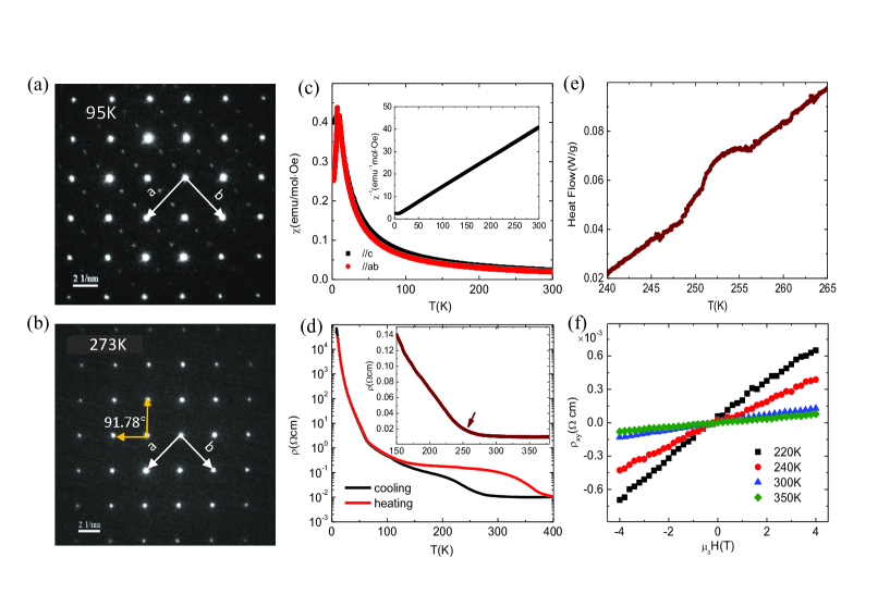
The low-temperature TEM study was employed to reveal further the morphologic distortions in EuTe4 system. Figure 3a shows the selected area electron diffraction (SAED) pattern of EuTe4 at 95 K along the [001] zone axis. The superlattice spots can be clearly differentiated only along [010] direction, showing a q-vector 0.33 b∗. The modulated lattice remains in an orthorhombic symmetry, consistent with the X-ray diffraction data. The TEM study also confirms that there is no superstructure existing for the pristine lattice at room temperature (Figure 3b).
The valence state of Eu in EuTe4 was analyzed by the magnetic property studies. Figure 3c shows the magnetic susceptibility of EuTe4, the data recognize an antiferromagnetic phase transition (TN = 7.1 K), arising from the in-plane correlation of magnetic moments of Eu ions. Above the Neel temperature, the susceptibility can be modeled using the Curie - Weiss law [ = 0 + C/(T - )] (Figure S3). The derived effective magnetic moment of 7.65 per Eu agrees well with the theoretical value of 7.9 for free Eu2+ ions. As will be discussed in the following DFT paragraph, the 4f electrons of Eu are strongly localized around -1.5 eV below the FS and the electronic bands near the FS are mainly from Te 5p orbitals. Therefore, the localized 4f electrons of Eu2+ are considered having no influence on the CDW order. Furthermore, owing to large magnetic moment, Eu2+ dominates the magnetic susceptibility in EuTe4 material. In our measurements, there is no anomaly observed in the measured magnetic susceptibility near the CDW transition, suggesting that the CDW's contribution of susceptibility is too small to be detected.
A well-defined semiconductive behavior was found for EuTe4. As is recognized from the temperature dependent in-plane electrical resistivity, for both cooling and heating process (Figure 3d). The large temperature hysteresis yields evidence for a first-order phase transition. The transition temperature Tc, defined from the resistivity kink of cooling process, is 255 K. Above Tc and as cooling, the resistivity shows a positive temperature-dependence and has a value 1.1 10-2 cm at RT, indicating a bad-metal characteristic. While below Tc, the resistivity manifests a thermally activated semiconductive behavior. The slope of the logarithm resistivity vs 1000/T plot at low temperatures gives an activation energy of 25 meV (see Figure S4). The resistivity also shows a kink at 50K, which might be related to a further structural change in the system beyond our experimental determination. Differential scanning calorimetry on a large number of crystals shows a kink around the same temperature, consistent with the existence of the first-order phase transition in the bulk (Figure 3e).
Hall effect measurements were conducted on the same single crystal from which the resistivity was measured (Figure 3f), which give rise to a p-type charge conduction with carrier concentrations estimated to be 3.1 1019 cm-3, 1.9 1019 cm-3, 6.2 1018 cm-3 and 3.7 1018 cm-3 at 350 K, 300 K, 240 K, 220 K respectively based on one-type carrier model. The calculated carriers mobility, for instance, is 36 cm2 V-1 s-1 at 300K and 42 cm2 V-1 s-1 at 220 K. These results imply that EuTe4 is a semiconductor having low carrier concentrations, in contrast to the common trivalent rare-earth species Ten which are metals with higher carriers densities Min et al. (2002); Ru and Fisher (2006).
In order to understand the origin of the structural phase transition, we have performed the electronic structures calculations based on the RT structure of EuTe4 by the density functional theory (DFT) method. The BSTATE (Beijing Simulation Tool of Atomic TEchnology) packageFang and Terakura (2002) with plane-wave pseudopotential method implemented was used for DFT calculations, all results are double-checked by the projector augmented wave methodBlöchl (1994); Kresse and Joubert (1999) implemented in VASP packageKresse and Furthmüller (1996). The calculated total and projected density of states (DOS and PDOS) for the nonmagnetic state are plotted in Figure 4a, which shows that the states between eV and eV are mostly contributed by the and orbitals of Te atoms. In order to figure out which kinds of Te atoms dominate near the Fermi level, the projected band structures for different kinds of Te atoms are plotted in Figure 4b, which indicate that the low-energy bands can be schematically separated into two parts. The narrow bands below eV are mostly from and orbitals of Te(2) atoms, while the dispersive bands near the Fermi level are mainly contributed by the and orbitals from Te(3), Te(4) and Te(5) atoms. Such results demonstrate a metallic and anisotropic electronic structures for the RT EuTe4, where the metallic electrons mainly come from the and orbitals of the Te square sheets, i.e., Te(3), Te(4) and Te(5) atoms.
Such anisotropy can also be reflected by the calculated two-dimensional like Fermi surfaces (FSs), as shown in Figure 4c. There are three types of FSs in Figure 4c, three concave-square hole FSs around the point (blue FSs surrounding ), six spindle-shape electron FSs around the X and Y points (three red FSs surrounding X and three red FSs surrounding Y), and three convex-square hole FSs around the S point (blue FSs surrounding the corner). It's obvious that there are two vectors that can induce large FSs nesting effect, i.e., by shifting the FSs of and , both can lead to the significant overlap of the FSs. In order to clarify which vector is favored, we calculated the Lindhard response functionDong et al. (2008); Johannes and Mazin (2008), and plotted the normalized two-dimensional Lindhard response function in Figure 4d, where the value of , i.e., the brightness in Figure 4d, can be used to quantitatively estimate the strength of the nesting effect. The calculated is more strongly peaked at than that at , which can also be demonstrated by the normalized one-dimensional as shown in Figure 4e. In Figure 4e, we have also plotted the normalized one-dimensional along different vectors, such as , and (whose corresponding to 132 reconstruction in the real space). We find that the biggest appears at or , which demonstrates two important facts. Firstly, the FSs of RT EuTe4 are quite two-dimensional. Secondly, the nesting effect induced by the shifting is responsible for the 13 reconstruction of the Te square sheets, which agrees well with the experimental observation of the in-plane supercell vector.
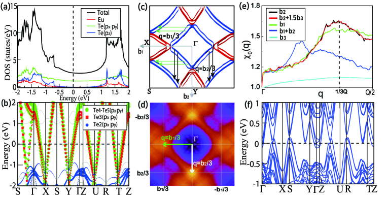
The good two-dimensional character of the FSs makes a nearly perfect nesting vector. In Figure S5b, we plot a schematic of FSs nesting by vector, where all the original FSs (solid curves in red and blue) in the reconstructed Brillouin zone (BZ, the area between the black dashes) are nested with the folded FSs (dashed curves in red and blue) almost perfectly. Such strong nesting effect by the vector suggests that most the FSs will be gapped after the () superlattice reconstruction, which is also confirmed by our electric structures calculations on the low-temperature structure (132). In Figure 4f, we plot the band structures calculated based on the experimental low-temperature structure and the generalized gradient approximation (GGA)Perdew et al. (1996) type of the exchange-correlation potential. Comparing with Figure 4a-4c, the FSs is much smaller for the low-temperature structure, and its DOS at the Fermi level is reduced to 0.63 states/(eV f.u.) (1.38 states/(eV f.u.) for the RT structure), indicating that most FSs are gapped by the (13) reconstruction. And the total energy of LT structure is about 4 meV/f.u. lower than that of the RT structure due to the FSs nesting. As we know, GGA usually overestimates the overlap of the conduction bands and the valence bands. The nonlocal Heyd-Scuseria-Ernzerhof (HSE06) hybrid functional calculations Heyd et al. (2003) can partially overcome this flaw. We have performed HSE06 calculations on the low-temperature structure of EuTe4. The DOS at the Fermi level, as shown in Figure S5c, is further reduced to 0.35 states/(eV f.u.). This may explain why the transport measurement of EuTe4 exhibits an insulating behavior at low temperature.
III conclusion
A new compound of binary rare-earth telluride EuTe4 is synthesized, which contains Te atomic quasi-square sheets. Eu is divalent, an only exceptional species among the layered RTen (n 2) polytellurides where R is normally trivalent, to the best of our knowledge. At RT, EuTe4 has a crystal structure containing two crystallographic inequivalent Te quasi-square sheets, each of them has strong CDW modulations after the Peierls transition. Unlike common 2D CDW systems which have metallic CDW state, EuTe4 has a semiconducting CDW phase. Detailed DFT calculations indicate that the FS topology of EuTe4 favors a nesting vector with a value of q = b∗/3 , corresponding closely with the experimental detected superstructure vector. Our results suggest a nesting driven CDW phase for EuTe4 material at cooling temperatures, which is responsible for the semiconducting state.
IV acknowledgement
This work was supported by the National Science Foundation of China (Nos. 11888101, 51502007 and 51672007), the National Key Research and Development Program of China (nos. 2017YFA0302904, 2016YA0300902, 2016YFA0300903, 2016YFA0300804 and 2018YFA0307000). We gratefully acknowledge Microscopy Laboratory in Peking University for the use of Cs corrected electron microscope and in situ TEM platform.
References
- Grüner (1988) G. Grüner, ``The dynamics of charge-density waves,'' Rev. Mod. Phys. 60, 1129–1181 (1988).
- Monceau (2012) Pierre Monceau, ``Electronic crystals: an experimental overview,'' Advances in Physics 61, 325–581 (2012).
- Ajisaka et al. (2009) Shigeru Ajisaka, Hisashi Nishimura, Shuichi Tasaki, and Ichiro Terasaki, ``Nonequilibrium peierls transition,'' Progress of Theoretical Physics 121, 1289–1319 (2009).
- Wu et al. (2011) Tao Wu, Hadrien Mayaffre, Steffen Krämer, Mladen Horvatić, Claude Berthierl, W. N. Hardy, Ruixing Liang, D. A. Bonn, and Marc Henri Julien, ``Magnetic-field-induced charge-stripe order in the high-temperature superconductor YBa2Cu3Oy,'' Nature 477, 191–194 (2011), 1109.2011 .
- Kawasaki et al. (2017) S. Kawasaki, Z. Li, M. Kitahashi, C. T. Lin, P. L. Kuhns, A. P. Reyes, and Guo Qing Zheng, ``Charge-density-wave order takes over antiferromagnetism in Bi2Sr2-xlaxCuO6superconductors,'' Nature Communications 8, 4–10 (2017), 1704.06169 .
- Chang et al. (2012) J. Chang, E. Blackburn, A. T. Holmes, N. B. Christensen, J. Larsen, J. Mesot, Ruixing Liang, D. A. Bonn, W. N. Hardy, A. Watenphul, M. V. Zimmermann, E. M. Forgan, and S. M. Hayden, ``Direct observation of competition between superconductivity and charge density wave order in YBa2Cu3O6.67,'' Nature Physics 8, 871–876 (2012).
- Colonna et al. (2005) Stefano Colonna, Fabio Ronci, Antonio Cricenti, Luca Perfetti, Helmuth Berger, and Marco Grioni, ``Mott Phase at the Surface of 1T-TaSe2 Observed by Scanning Tunneling Microscopy,'' Phys. Rev. Lett. 94, 036405 (2005).
- Sipos et al. (2008) B. Sipos, A. F. Kusmartseva, A. Akrap, H. Berger, L. Forró, and E. Tutǐ, ``From Mott state to superconductivity in 1T-TaS2,'' Nature Materials 7, 960–965 (2008).
- Kidd et al. (2002) T. E. Kidd, T. Miller, M. Y. Chou, and T.-C. Chiang, ``Electron-Hole Coupling and the Charge Density Wave Transition in TiSe2,'' Phys. Rev. Lett. 88, 226402 (2002).
- Li et al. (2007) G. Li, W. Z. Hu, D. Qian, D. Hsieh, M. Z. Hasan, E. Morosan, R. J. Cava, and N. L. Wang, ``Semimetal-to-Semimetal Charge Density Wave Transition in 1T-TiSe2,'' Phys. Rev. Lett. 99, 027404 (2007).
- Malliakas et al. (2008) Christos D. Malliakas, Maria Iavarone, Jan Fedor, and Mercouri G. Kanatzidis, ``Coexistence and Coupling of Two Distinct Charge Density Waves in Sm2Te5,'' Journal of the American Chemical Society 130, 3310–3312 (2008).
- Hu et al. (2014) B. F. Hu, B. Cheng, R. H. Yuan, T. Dong, and N. L. Wang, ``Coexistence and competition of multiple charge-density-wave orders in rare-earth tritellurides,'' Phys. Rev. B 90, 085105 (2014).
- Gweon et al. (1998) G.-H. Gweon, J. D. Denlinger, J. A. Clack, J. W. Allen, C. G. Olson, E. DiMasi, M. C. Aronson, B. Foran, and S. Lee, ``Direct Observation of Complete Fermi Surface, Imperfect Nesting, and Gap Anisotropy in the High-Temperature Incommensurate Charge-Density-Wave Compound SmTe3,'' Phys. Rev. Lett. 81, 886–889 (1998).
- Brouet et al. (2004) V. Brouet, W. L. Yang, X. J. Zhou, Z. Hussain, N. Ru, K. Y. Shin, I. R. Fisher, and Z. X. Shen, ``Fermi Surface Reconstruction in the CDW State of CeTe3 Observed by Photoemission,'' Phys. Rev. Lett. 93, 126405 (2004).
- Patschke and Kanatzidis (2002) Rhonda Patschke and Mercouri G. Kanatzidis, ``Polytelluride compounds containing distorted nets of tellurium,'' Phys. Chem. Chem. Phys. 4, 3266–3281 (2002).
- Papoian and Hoffmann (2000) Garegin A Papoian and Roald Hoffmann, ``Hypervalent bonding in one, two, and three dimensions- extending the zintl-klemm concept to nonclassical electron-rich networks,'' Angewandte Chemie International Edition 39, 2408–2448 (2000).
- Malliakas et al. (2005) Christos Malliakas, Simon J L Billinge, Jeong Kim Hyun, and Mercouri G. Kanatzidis, ``Square nets of tellurium: Rare-earth dependent variation in the charge-density wave of RETe3 (RE = Rare-Earth Element),'' Journal of the American Chemical Society 127, 6510–6511 (2005).
- Schmitt et al. (2008) F. Schmitt, P. S. Kirchmann, U. Bovensiepen, R. G. Moore, L. Rettig, M. Krenz, J.-H. Chu, N. Ru, L. Perfetti, D. H. Lu, M. Wolf, I. R. Fisher, and Z.-X. Shen, ``Transient Electronic Structure and Melting of a Charge Density Wave in TbTe3,'' Science 321, 1649–1652 (2008).
- Kim et al. (2006) H. J. Kim, C. D. Malliakas, A. T. Tomić, S. H. Tessmer, M. G. Kanatzidis, and S. J. L. Billinge, ``Local Atomic Structure and Discommensurations in the Charge Density Wave of CeTe3,'' Phys. Rev. Lett. 96, 226401 (2006).
- Min et al. (2002) B.H. Min, E.D. Moon, H.J. Im, S.O. Hong, Y.S. Kwon, D.L. Kim, and H.-C. Ri, ``Transport properties in low carrier system CeTe2,'' Physica B: Condensed Matter 312-313, 205 – 207 (2002).
- Shin et al. (2005) K. Y. Shin, V. Brouet, N. Ru, Z. X. Shen, and I. R. Fisher, ``Electronic structure and charge-density wave formation in LaTe1.95 and CeTe2.00,'' Phys. Rev. B 72, 085132 (2005).
- Kwon and Min (2000) Y S Kwon and B H Min, ``Anisotropic transport properties in RTe2 ( R : La , Ce , Pr , Sm and Gd ),'' Physica B 282, 281–282 (2000).
- Huang et al. (2012) Y. Huang, B. F. Hu, T. Dong, A. F. Fang, P. Zheng, and N. L. Wang, ``Effect of disorder in the charge-density-wave compounds LaTe 1.95 and CeTe 1.95-xSe x (x=0 and 0.16) as revealed by optical spectroscopy,'' Physical Review B - Condensed Matter and Materials Physics 86, 1–6 (2012).
- Lavagnini et al. (2007) M. Lavagnini, A. Sacchetti, L. Degiorgi, K. Y. Shin, and I. R. Fisher, ``Optical properties of the Ce and La ditelluride charge density wave compounds,'' Phys. Rev. B 75, 205133 (2007).
- Tremel and Hoffmann (1987) Wolfgang Tremel and Roald Hoffmann, ``Square nets of main-group elements in solid-state materials,'' Journal of the American Chemical Society 109, 124–140 (1987).
- Ru and Fisher (2006) N. Ru and I. R. Fisher, ``Thermodynamic and transport properties of YTe3, LaTe3, and CeTe3,'' Phys. Rev. B 73, 033101 (2006).
- Fang and Terakura (2002) Zhong Fang and Kiyoyuki Terakura, ``Structural distortion and magnetism in transition metal oxides: crucial roles of orbital degrees of freedom,'' Journal of Physics: Condensed Matter 14, 3001 (2002).
- Blöchl (1994) P. E. Blöchl, ``Projector augmented-wave method,'' Phys. Rev. B 50, 17953–17979 (1994).
- Kresse and Joubert (1999) G. Kresse and D. Joubert, ``From ultrasoft pseudopotentials to the projector augmented-wave method,'' Phys. Rev. B 59, 1758–1775 (1999).
- Kresse and Furthmüller (1996) G. Kresse and J. Furthmüller, ``Efficiency of ab-initio total energy calculations for metals and semiconductors using a plane-wave basis set,'' Computational Materials Science 6, 15 – 50 (1996).
- Dong et al. (2008) J. Dong, H. J. Zhang, G. Xu, Z. Li, G. Li, W..Z. Hu, D. Wu, G. F. Chen, X. Dai, J. L. Luo, Z. Fang, and N. L. Wang, ``Competing orders and spin-density-wave instability in La (O1- xFx) FeAs,'' EPL (Europhysics Letters) 83, 27006 (2008).
- Johannes and Mazin (2008) M. D. Johannes and I. I. Mazin, ``Fermi surface nesting and the origin of charge density waves in metals,'' Phys. Rev. B 77, 165135 (2008).
- Perdew et al. (1996) John P. Perdew, Kieron Burke, and Matthias Ernzerhof, ``Generalized gradient approximation made simple,'' Phys. Rev. Lett. 77, 3865–3868 (1996).
- Heyd et al. (2003) Jochen Heyd, Gustavo E. Scuseria, and Matthias Ernzerhof, ``Hybrid functionals based on a screened Coulomb potential,'' Journal of Chemical Physics 118, 8207–8215 (2003).