Full control of quantum Hall supercurrent in a side gated graphene Josephson junction
Abstract
We present a study of a graphene-based Josephson junction with dedicated side gates carved from the same sheet of graphene as the junction itself. These side gates are highly efficient, and allow us to modulate carrier density along either edge of the junction in a wide range. In particular, in magnetic fields in the Tesla range, we are able to populate the next Landau level, resulting in Hall plateaus with conductance that differs from the bulk filling factor. When counter-propagating quantum Hall edge states are introduced along either edge, we observe supercurrent localized along that edge of the junction. Here we study these supercurrents as a function of magnetic field and carrier density.
The interplay of spin-helical states and superconductivity is predicted to enable access to non-Abelian excitations such as Majorana zero modes (MZM) Alicea ; Fu2 ; Lutchyn ; Oreg . Through braiding operations which reveal nontrivial exchange statistics, these states may form the basis for quantum computing architectures which take advantage of topological protections to achieve fault-tolerance Nayak . Several technologies to this end are in development, including hybrid superconductor-semiconducting nanowire and superconductor-topological insulator structures Lutchyn2 ; Aguado . Interest in topological superconductivity has also spurred a flurry of activity at the interface of superconductivity and the quantum Hall (QH) effect Amet ; Shalom ; Draelos ; Seredinski ; Calado ; Wan ; Lee ; Park ; Sahu . It has been predicted that quasi-1D superconducting contacts to a QH structure could enable MZM and parafermions Clarke1 ; Clarke2 ; Mong .
Heterostructures of graphene and hexagonal boron nitride with one-dimensional superconducting contacts Calado can demonstrate a remarkable contact transparency, allowing us to observe supercurrent in the quantum Hall regime Amet . However, the microscopic details of the supercurrent in the QH regime remain an open subject Draelos . In particular, the nature of the superconducting coupling to the edge states could depend e.g. on the vacuum edges of the graphene mesa, the drift velocity of the QH edge states, or the presence of incompressible strips. Yet, the electrostatic potential along the mesa edge is typically poorly controlled; it is known to be influenced by charge accumulation effects Silvestrov , and may be strongly affected by the disorder resulting from physical etching. Here, we examine a graphene Josephson junction with two side gates that allow us to directly manipulate the QH edge states. By tuning either gate, we can change the Landau level (LL) filling factor along the edges in a wide range. We controllably induce counter-propagating states along either edge and observe supercurrent localized solely along one edge. This technique holds promise for making future devices which would allow one to create and manipulate MZM and parafermions along the lines proposed in Clarke1 ; Clarke2 .
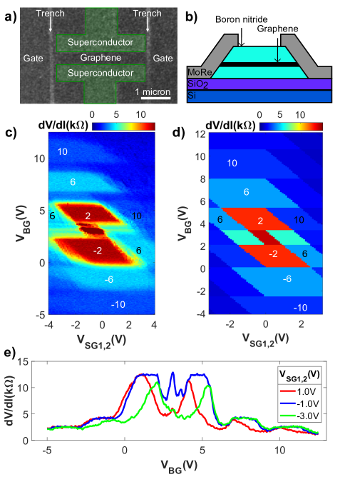
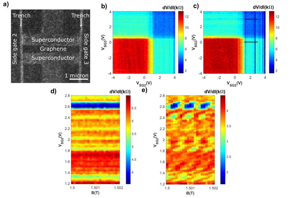
Our samples are made from graphene encapsulated in hexagonal boron nitride (BN), which protects devices from processing contamination and can yield ballistic transport over micron scales Mayorov . The graphene-BN stack is then etched, and quasi-one dimensional contacts to the exposed regions are fabricated Dean . We use molybdenum rhenium (MoRe), a type-II superconductor with an upper critical field of at least 9 T and critical temperature of K. The m wide contacts are separated by 500 nm and are initially made to an extended region of graphene. At the next stage, both the junction and the side gates are formed by etching narrow trenches on each side of the contacts (Figure 1a). Applying voltage to the graphene regions that form the side gates allows us to efficiently control the electron density along the edges of the junction. It is important that the etched trenches do not overlap with the contacts, and are instead spaced from them by a graphene strip 100 nm wide. This strip separates the contacts from any atomic-scale spurious states that may exist along the etched edge. For consistency, we present results from one Josephson junction; additional measurements of a second device are shown in the supplementary.
I Side gate influence in the quantum Hall regime
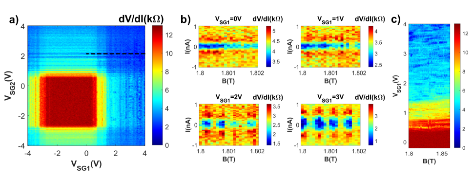
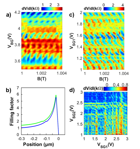
As a magnetic field is applied perpendicular to the sample, the junction enters the quantum Hall regime. By 1.8 T, the quantum Hall effect is very well developed and we stay at that field in Figures 1-3. The influence of the side gates is significant in this regime, since the edges of the device dominate the transport properties. Figure 1c maps the influence of the back gate and the two side gates, applied symmetrically, . This and subsequent measurements in this section are performed with a DC bias current of 10 nA, enough to suppress any supercurrent that may be flowing between the contacts in the QH regime. An additional, negligibly small AC current of 50 pA is applied in order to measure the differential resistance with a lock-in amplifier. The large central red (high resistance) features in Figure 1c mark the quantum Hall plateaus. Above and below these are the standard states. Only the sequence of filling factors is visible at this field.
The regions of quantized conductance have a diamond shape, whose boundaries in the back gate direction are flat (horizontal), which means that they are not affected by the side gates. The inclined side boundaries of the red diamonds indicate that they depend both on the side gates and the back gate. These boundaries are interpreted as a line of constant carrier density along the edges of the device, where is a constant determined by the relative gate efficiencies. The overall shape of the map in Figure 1c is well reproduced by a simple electrostatic simulation, as shown in Figure 1d.
Finally, the centers of diamond-shaped plateaus in Figure 1c are shifted from V indicating that the “neutral” side gate voltage is close to -1 V. This differs from the back gate position of the charge neutrality point (3.5 V) not only in magnitude but in polarity, indicating a carrier buildup along the edges of the junction distinct from the doping of the bulk. The side gate influence is illustrated in Figure 1e, which demonstrates that the resistance plateaus of the device, as a function of back gate, are better formed at V than at -3 V or +1 V.
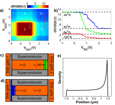
More insight into the device’s phenomenology is gained by applying the side gates independently. Figure 2a shows a resistance map of the device as a function of both side gates at 4.7 V. (Taking a diagonal line in Figure 2a would corresponds to a horizontal line going through the middle of the diamond in Figure 1c.) The prominent feature of Figure 2a is a square central region with resistance quantized at . When either side gate is applied beyond the plateau region, the resistance drops to a new quantized value.
The observed influence of the side gates on the quantum Hall conductances is similar to the impact of local out-of-plane gates Tovari ; Ozyilmaz . The fact that the features in Figure 2a are purely horizontal or vertical shows that the influence of the two side gates is highly local: the left gate has a negligible effect on the right edge, and vice versa. This negligible cross-talk is different from that typically found in samples with out-of-plane gates. Furthermore, the side gates are very efficient, allowing us to control the filling factor of either edge in a wide range.
Figure 2b shows that the measured resistance drops from to if a positive side gate voltage is applied (green curve, measured along the green line in Figure 2a). This corresponds to , the local filling factor on the side close to side gate 2 (SG2), reaching as shown schematically in Figure 2c. The bulk filling factor remains at and an additional conductance of is contributed by the additional four-fold degenerate edge states induced near SG2. Note that in this case, the spatial separation between counterpropagating QH states in the side-gated region is less than 100 nm, as detailed further in the text. The observation of quantized resistance plateaus suggests that backscattering between these counter-propagating states is suppressed, despite their close proximity. However, this should not be surprising, given that robust quantum Hall plateaus were previously observed in graphene nanoribbons of comparable width Morpurgo2012 ; Molenkamp2012 .
Next, the red line of Figure 2b demonstrates that each side gate can induce an independent state along its edge. Here SG1 is fixed at 3 V; this corresponds to a local filling factor near SG1 of . Before SG2 is applied we start with resistance of : the baseline conductance is and the right edge contributes additional , much like at the end point of the green curve in Figure 2b. Applying SG2 then adds an additional four-fold-degenerate channel on the other edge of the sample, resulting in the drop of resistance to , which corresponds to conductance of .
Finally, we tune the back gate to 1.5 V (instead of 4.7 V), resulting in a bulk filling of . Applying SG1 now yields a transition from to (blue curve in Figure 2b.) The schematics in Figure 2d shows that in this case the side gate locally induces a QH state with an opposite filling factor of , and the resulting plateau has a conductance of . Note that here as well, counterpropagating states are created in close proximity to each other.
II Side gates and quantum Hall supercurrent
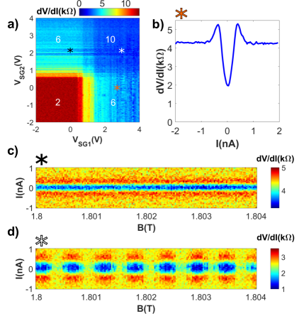
So far, the measurements have been performed with an applied DC bias current of 10 nA to suppress any supercurrent. We now switch to zero and explore the emerging superconducting features, maintaining the small AC current of 50 pA used to measure the differential resistance. Figure 3a shows a map of sample resistance vs. side gates similar to that in Figure 2a. While no supercurrent is found on top of the plateau, once the state is induced by either side gate the sample resistance develops pronounced dips that were not present at high DC current.
Figure 3b shows the sample resistance vs. bias taken at the location in Figure 3a marked by an orange asterisk, corresponding to V and V, so that is close to bulk filling and . The region of suppressed resistance flanked by peaks is characteristic of a small supercurrent washed by thermal fluctuations. Notice that when the density enhancement is induced on one side only (regions in Figure 3a corresponding to the normal resistance of ) the supercurrent features appear as horizontal/vertical lines - they depend on one side gate and do not vary with the other side gate. This confirms that the supercurrent is localized at one side of the junction.
Furthermore, the supercurrent does not vary for small changes in magnetic field (Figure 3c), indicating that the area it encompasses does not enclose additional flux quanta for a few mT change in field. This observation limits the distance between the counterpropagating edge channels responsible for the supercurrent to no more than nm (see also Supplementary Figure S1c). This distance is comparable to the coherence length of MoRe, which facilitates the coupling of the edge states to the superconductor and explains the appearance of supercurrent when a side-gate is turned on.
The dependence of the supercurrent on magnetic field completely changes when both side gates are applied, creating supercurrents along the two edges of the sample. Figure 3d shows a map similar to Figure 3c but with both side gates applied ( V, V, marked by a white asterisk in Figure 3a). The map demonstrates a SQUID-like interference pattern with a period of 0.6 mT, close to that of the low-field Fraunhofer pattern of this junction (0.7 mT).
We explore the supercurrent interference pattern in the QH regime as a function of gate voltages in Figure 4. Here, we change the field to 1 T in order to observe a more robust superconducting signature. Figure 4a shows the pattern of resistance oscillations in magnetic field, measured at zero applied DC bias as a function of the back gate. The period of the oscillations is found to be the same as in Figure 3d and independent of the gate voltage. The phase of the oscillations, however, is seen to vary with gate with an approximate slope of /T.
This gradual shift of the magnetic interference pattern with the back gate is explained by the fact that the changing electron density shifts the position of the QH edge states, thereby changing the area between the supercurrents on the two sides. Interestingly, the phase change from an increase of density (at more positive ) is compensated for by the increase of the magnetic field, indicating that the effective area of the SQUID shrinks. This behavior can be understood from the schematic in Figure 4b, where the blue curve (lower back gate voltage) is compared to the green line (higher back gate voltage). The counterpropagating edge states occur on the opposite slopes of the non-monotonic density profile close to each edge. As the overall density increases (from the blue to the green curve), the inner states move further inward, while the outer states stay relatively stationary due to the very high density gradient close to the sample edge. As a result, on average the location of the supercurrent moves inward with increasing density.
A similar change in the interference pattern is observed when a side gate is applied (Figure 4c). The slope of this pattern is roughly . Notably, the sign of the slope in Figures 4c is flipped compared to the one seen in Figure 4a. Following the discussion in the previous paragraph, this slope suggests that applying the side gate may be increasing the effective area of the SQUID. This could likely be attributed to the outward shift of the outer edge state, which is more strongly influenced by the side gate than the inner edge state. The very small size of the graphene region affected by the side gate might also result in charging effects, which are known to invert the slope of fringes in quantum Hall interferometers Marcus2009 ; Ofek2010 ; Halperin2011 .
Finally, an additional interference pattern is revealed in Figure 4d, which shows the sample resistance as a function of both side gates ( T). The interference is visible at the intersections of the vertical and horizontal lines corresponding to supercurrents flowing along the SG1 and SG2 edges, respectively. The interpretation of this interference pattern is similar to the discussion above, with each gate affecting the location of the edge state on its side of the device. The contours of constant phase at the intersections of the vertical and horizontal lines have a roughly diagonal slope, indicating that the two gates have comparable efficiency.
III Discussion
We have shown that native graphene side gates are remarkably efficient in controlling edge state propagation in the quantum Hall regime. They enable full control of the local filling factors along the sample edges, allowing us to fill the next Landau level, change carrier polarity, or keep the density flat close to the edge. Further, we have observed supercurrents carried by the QH edge states induced by the side gates. These supercurrents flow independently on each edge of the device and could be controlled independently by the corresponding gates. Our experiment opens a promising route for coupling superconductors with QH edge states for the purpose of inducing non-Abelian excitations.
IV Methods
The sample was made with mechanically exfoliated flakes of graphene and hexagonal boron nitride. It was assembled using a standard stamping technique Wang . The resulting heterostructure was patterned using electron beam lithography followed by reactive ion etching with and to expose the edges of the encapsulated graphene. These edges were contacted with nm of molybdenum rhenium (50-50 ratio by weight) sputtered onto the etched regions. The device boundaries and sidegates were defined with a second round of lithography and etching.
Measurements were performed in a Leiden Cryogenics dilution refrigerator at a temperature of mK. The sample was electronically isolated in the refrigerator via resistive coax lines and low-temperature RC filters. Differential resistance measurements were carried out using an AC excitation current of 50pA. Magnetic fields for quantum Hall measurements were applied perpendicular to the sample plane.
V Data availability
The datasets supporting the figures and conclusions of the current study are available from the corresponding author upon request.
VI Acknowledgments
We thank Harold Baranger, Ady Stern, and Enrico Rossi for helpful discussions. Transport measurements conducted by A.S., A.W.D., and E.G.A. were supported by Division of Materials Sciences and Engineering, Office of Basic Energy Sciences, U.S. Department of Energy, under Award No. DE- SC0002765. A.S. and M.T.W. performed lithographic fabrication and characterization of the samples with the support of NSF awards ECCS-1610213 and DMR-1743907. G.F. was supported under ARO Award W911NF16-1-0122. H.L. and F.A. acknowledge the ARO under Award W911NF-16-1-0132. K.W. and T.T. acknowledge support from JSPS KAKENHI Grant Number JP15K21722 and the Elemental Strategy Initiative conducted by the MEXT, Japan. T.T. acknowledges support from JSPS Grant-in-Aid for Scientific Research A (No. 26248061) and JSPS Innovative Areas “Nano Informatics” (No. 25106006). This work was performed in part at the Duke University Shared Materials Instrumentation Facility (SMIF), a member of the North Carolina Research Triangle Nanotechnology Network (RTNN), which is supported by the National Science Foundation (Grant ECCS-1542015) as part of the National Nanotechnology Coordinated Infrastructure (NNCI).
VII Author Contributions
A.S., F.A., and G.F. designed the project and experiments. A.S., A.W.D., and E.G.A. conducted measurements and analyzed the data. G.F. supervised the experiments. K.W. and T.T. provided the crystals of hexagonal boron nitride. H.L. and F.A. assembled the graphene / boron nitride heterostructure. A.S. and M.T.W. fabricated the device. A.S., F.A., and G.F. wrote the manuscript.
VIII Competing financial interests
The authors declare no competing financial interests.
References
- (1) L. Fu and C.L. Kane. Josephson current and noise at a superconductor/quantum-spin-Hall-insulator/superconductor junction. Phys. Rev. B 79, 161408 (2009).
- (2) R.M. Lutchyn, J.D. Sau, and S. Das Sarma. Majorana Fermions and a Topological Phase Transition in Semiconductor-Superconductor Heterostructures. Phys. Rev. Lett. 105, 077001 (2010).
- (3) Y. Oreg, G. Rafael, and F. von Oppen. Helical Liquids and Majorana Bound States in Quantum Wires. Phys. Rev. Lett. 105, 177002 (2010).
- (4) J. Alicea. New directions in the pursuit of Majorana fermions in solid state systems. Rep. Prog. Phys. 75, 076501 (2012).
- (5) C. Nayak, S.H. Simon, A. Stern, M. Freedman, and S. Das Sarma. Non-Abelian anyons and topological quantum computation. Rev. Mod. Phys. 80, 1083 (2008).
- (6) R.M. Lutchyn, E.P.A.M. Bakkers, L.P. Kouwenhoven, P. Krogstrup, C.M. Marcus, Y. Oreg. Majorana zero modes in superconductor-semiconductor heterostructures. Nat. Rev. Mater. 3, 52-68 (2018).
- (7) R. Aguado. Majorana quasiparticles in condensed matter. Riv. Nuovo Cimento 40, 523 (2017).
- (8) Z. Wan, A. Kazakov, M.J. Manfra, L.N. Pfeiffer, K.W. West, and L.P. Rokhinson. Induced superconductivity in high-mobility two-dimensional electron gas in gallium arsenide heterostructures. Nat. Comm. 6, 7426 (2015).
- (9) V.E. Calado, S. Goswami, G. Nanda, M. Diez, A.R. Akhmerov, K. Watanabe, T. Taniguchi, T.M. Klapwijk, and L.M.K. Vandersypen. Ballistic Josephson junctions in edge-contacted graphene. Nat. Nanotech. 10, 761-764 (2015).
- (10) F. Amet, C.T. Ke, I.V. Borzenets, J. Wang, K. Watanabe, T. Taniguchi, R.S. Deacon, M. Yamamoto, Y. Bomze, S. Tarucha, and G. Finkelstein. Supercurrent in the quantum Hall regime. Science 352, 6288 (2016).
- (11) M. Ben Shalom, M.J. Zhu, V.I. Fal’ ko, A. Mishchenko, A.V. Kretinin, K.S. Novoselov, C.R. Woods, K. Watanabe, T. Taniguchi, A.K. Geim, and J.R. Prance. Quantum oscillations of the critical current and high-field superconducting proximity in ballistic graphene. Nat. Phys. 12, 318-322 (2016).
- (12) G.H. Lee, K.F. Huang, D.K. Efetov, D.S. Wei, S. Hart, T. Taniguchi, K. Watanabe, A. Yacoby, and P. Kim. Inducing superconducting correlation in quantum Hall edge states. Nature Physics 13, 693-698 (2017).
- (13) G.H. Park, M. Kim, K. Watanabe, T. Taniguchi, and H.J. Lee. Propagation of superconducting coherence via chiral quantum-Hall edge channels. Sci. Rep. 7, 10953 (2017).
- (14) A. W. Draelos, M.T. Wei, A. Seredinski, C.T. Ke, Y. Mehta, R. Chamberlain, K. Watanabe, T. Taniguchi, M. Yamamoto, S. Tarucha, I.V. Borzenets, F. Amet, and G. Finkelstein. Investigation of Supercurrent in the Quantum Hall Regime in Graphene Josephson Junctions. J. Low Temp. Phys. 191, 288-300 (2018).
- (15) A. Seredinski, A. Draelos, M.T. Wei, C.T. Ke, T. Fleming, Y. Mehta, E. Mancil, H. Li, T. Taniguchi, K. Watanabe, S. Tarucha, M. Yamamoto, I.V. Borzenets, F. Amet, and G. Finkelstein. Supercurrent in Graphene Josephson Junctions with Narrow Trenches in the Quantum Hall Regime. MRS Advances 3, 2855-2864 (2018).
- (16) M.R. Sahu, X. Liu, A.K. Paul, S. Das, P. Raychaudhuri, J.K. Jain, and A. Das. Inter-Landau-level Andreev Reflection at the Dirac Point in a Graphene Quantum Hall State Coupled to a Superconductor. Phys. Rev. Lett. 121, 086809 (2018).
- (17) D.J. Clarke, J. Alicea, and K. Shtengel. Exotic non-Abelian anyons from conventional fractional quantum Hall states. Nat. Comm. 4, 1348 (2013).
- (18) D.J. Clarke, J. Alicea, and K. Shtengel. Exotic circuit elements from zero-modes in hybrid superconductor–quantum-Hall systems. Nat. Phys. 10, 877-882 (2014).
- (19) R.S.K. Mong, D.J. Clarke, J. Alicea, N.H. Lindner, P. Fendley, C. Nayak, Y. Oreg, A. Stern, E. Berg, K. Shtengel, and M.P.A. Fisher. Universal Topological Quantum Computation from a Superconductor-Abelian Quantum Hall Heterostructure. Phys. Rev. X 4, 011036 (2014).
- (20) P.G. Silvestrov and K.B. Efetov. Charge accumulation at the boundaries of a graphene strip induced by a gate voltage: Electrostatic approach. Phys. Rev. B 77, 155436 (2008).
- (21) C.R. Dean, A.F. Young, I. Meric, C. Lee, L. Wang, S. Sorgenfrei, K. Watanabe, T. Taniguchi, P. Kim, K.L. Shepard, and J. Hone. Boron nitride substrates for high-quality graphene electronics. Nat. Nanotech. 5, 722-726 (2010).
- (22) A.S. Mayorov, R.V. Gorbachev, S.V. Morozov, L. Britnell, R. Jalil, L.A. Ponomarenko, P. Blake, K.S. Novoselov, K. Watanabe, T. Taniguchi, and A.K. Geim. Micrometer-Scale Ballistic Transport in Encapsulated Graphene at Room Temperature. Nano Lett. 11 (6), 2396-2399 (2011).
- (23) E. Tóvári, P. Makk, M.H. Liu, P. Rickhaus, Z. Kovács-Krausz, K. Richter, C. Schönenberger, and S. Csonka. Gate-controlled conductance enhancement from quantum Hall channels along graphene pn junctions. Nanoscale 8, 19910 (2016).
- (24) B. Özyilmaz, P. Jarillo-Herrero, D. Efetov, D.A. Abanin, L.S. Levitov, and P. Kim. Electronic Transport and Quantum Hall Effect in Bipolar Graphene p-n-p Junctions. Phys. Rev. Lett. 99, 166804 (2007).
- (25) F. Duerr, J.B. Oostinga, C. Gould, and L.W. Molenkamp. Edge state transport through disordered graphene nanoribbons in the quantum Hall regime. Phys. Rev. B 86, 081410(R) (2012).
- (26) D.-K. Ki and A. F. Morpurgo. Crossover from Coulomb Blockade to Quantum Hall Effect in Suspended Graphene Nanoribbons. Phys. Rev. Lett. 108, 266601 (2012).
- (27) J.A.M. van Ostaay, A.R. Akhmerov, C.W.J. Beenakker. Spin-triplet supercurrent carried by quantum Hall edge states through a Josephson junction. Phys. Rev. B 83, 195441 (2011).
- (28) Y. Zhang, D. T. McClure, E. M. Levenson-Falk, C. M. Marcus, L. N. Pfeiffer, and K. W. West. Distinct signatures for Coulomb blockade and Aharonov-Bohm interference in electronic Fabry-Perot interferometers. Phys. Rev. B 79, 241304(R) (2009)
- (29) N. Ofek, A. Bid, M. Heiblum, A. Stern, V. Umansky, and D. Mahalu. Role of interactions in an electronic Fabry-Perot interferometer operating in the quantum Hall effect regime. PNAS 107 (12), 5276-5281 (2010).
- (30) B.I. Halperin, A. Stern, I. Neder, and B. Rosenow. Theory of Fabry-Pérot quantum Hall interferometer. Phys. Rev. B 83, 155440 (2011).
- (31) L. Wang, I. Meric, P.Y. Huang, Q. Gao, Y. Gao, H. Tran, T. Taniguchi, K. Watanabe, L.M. Campos, D.A. Muller, J. Guo, P. Kim, J. Hone, K.L. Shepard, and C.R. Dean. One-Dimensional Electrical Contact to a Two-Dimensional Material. Science 342, 6158 (2013).
Supplementary material: Full control of quantum Hall supercurrent in a side gated graphene Josephson junction
In support of the data presented the main paper, here we include additional measurements and types of differential resistance maps.
I Additional supercurrent interference maps
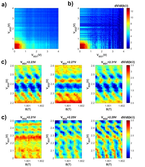
Figure S1 expands on the 1.8 T data presented in Figures 1-3 in the main text. Panel a shows a wider version of the SG1-SG2 map of differential resistance seen in Figure 3a with nA. Here, in addition to the side gate induced quantum Hall plateaus, we see lines of reduced resistance as supercurrent appears at certain side gate voltages on either side of the junction. The panels of Figure S1b show the magnetic interference pattern of one supercurrent pocket induced by SG2 as SG1 changes from 0 to +3 V, following the dashed line in Figure S1a. Once both gates are V, the supercurrents along the two edges interfere and we see the transition from an aperiodic to a fully SQUID-like interference pattern. Finally, Figure S1c shows aperiodic resistance measured as a function of magnetic field and SG1, with SG2 held at 0 V. This contrasts with the periodic side gate - field interference map taken in the regime when both edges carry supercurrent (Figure 4c). Clearly, since the supercurrent is independently controlled along each edge, only when both edges are active is there interference. As stated in the main text, we interpret the interference observed in Figure 4d as the result of each side gate tuning the location of its associated edge states, thus altering the enclosed magnetic flux through the junction.
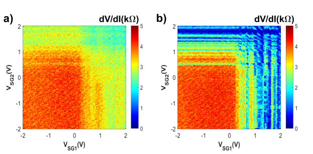
Figure S2 presents additional interference data at T. S2a and b contrast the differential resistance maps taken at nA and ; S2b is an extended version of the map in Figure 4d. It is clear that the map in S2a lacks the diagonal interference features present in S2b. Indeed, these features are attributed to interference of supercurrents, which are suppressed by nA. Figures S2c,d detail the transition of the side gate interference pattern from periodic to aperiodic as a function of each side gate. This is consistent with the picture of independent supercurrents on each edge of the device being present at only certain local gate voltages.
II Measurements around the bulk plateau
The main text focuses on data taken when the bulk of the sample is tuned to the plateau. In this section, we include complementary data taken at the plateau in the bulk, at T. In Figure S3a, increasing either side gate leads to the total differential resistance reaching . This indicates the addition of a fourfold degenerate state only along one side of the junction. Tuning the second gate, understandably, yields : Each side of the junction can be thought of as locally being in the state, while the bulk remains at . Each edge contributes in addition to the base conductance. Figure S3b presents a map of differential resistance at nA, showing a multitude of locations with superconducting pockets.
III Measurements of a second device
In this section we present measurements similar to those in the main paper, but taken on a different device (J2). The dimensions of J2 are similar to J1, and the junction region is also separated from the two side gates by nm - wide trenches. However, here the contacts are not spaced from the trenches by 100 nm regions of graphene, as was done in J1. This second device was fabricated on the same chip as the main device. In fact, SG2 is shared by both junctions (Figure S4a).
The data presented were taken at T with V in the center of the plateau. Side gate - side gate maps of differential resistance are presented in Figure S4b,c and show the development of new resistance plateaus at high side gate voltage. These correspond to when one side gate is applied, and to when both are applied. These values are explained by the appearance of channels along each side of the junction. (See Figure 2d in the main text.)
Like our main junction J1, this device shows regions of supercurrent in the nA bias map (Figure S4c). As seen previously in Figure S1d, the dependence of supercurrent on magnetic field also undergoes a transition from non-periodic to SQUID-like: compare Figure S4d, in which only SG2 gate is active, to Figure S4e, in which SG3 is also applied, resulting in interference.
IV Electrostatic Simulations
In order to simulate the carrier density profile induced by the side gate in the quantum Hall regime, we determined the geometric local capacitance between the graphene sheet and both the back gate and side gates.
We solve the Laplace equation for the electrostatic potential with Dirichlet boundary conditions at the back gate, side gates, and the graphene sheet. Both local capacitances are spatially varying and are stronger at the graphene edge as a result of electric field focusing.
The back gate and the intrinsic doping of the graphene sheet (determined experimentally by the location of the Dirac peak in a gate sweep of the device) were then used to determine the bulk carrier density in the graphene and subsequently the chemical potential.
Applying a positive voltage on the side gate tends to raise the graphene potential near the edge. At zero temperature the local graphene potential can be obtained by solving:
| (1) |
Here, we defined the density of states as a sum of Gaussians centered at the Landau level energies with a Landau level degeneracy :
| (2) |
where parametrizes the breadth of the Landau levels. The local carrier density is then:
| (3) |
The vanishing of the carrier density at the edge was artificially obtained by linearly bringing the density to zero at the edge over a length scale l. The length scale of the convergence was chosen to be on the order of the magnetic length (nm) and justified post hoc through comparison of the simulated and experimental gate maps. This behavior is of course a simplification and further theoretical work will be needed to understand the evolution of the carrier density in the few nanometers near the edge.
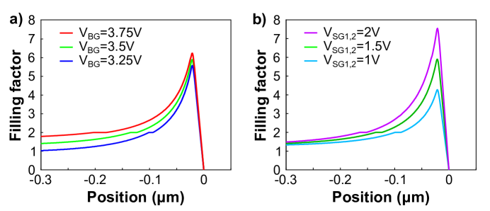
Figure S5 details the evolution of carrier density within 300nm of the junction edge with the application of back gate (Figure S5a) and side gate (Figure S5b) voltages. Figure S5a quantitatively builds on Figure 4b from the main text. We note that the electrostatic simulation of the side gate influence in Figure S5b does not reproduce the movement of the supercurrent carrying states towards the edge of the junction, as is discussed in the main text in explaining the slope of the interference pattern shown in Figure 4c.
Finally, to reproduce the differential resistance map shown in Figure 1c, the carrier density was used to determine the number of edge states in the system and plotted as a function of gate, generating Figure 1d. Commensurate with the integer plateaus seen in the experiment, we considered only the degenerate graphene filling factors () and added in the emerging peak (defined in the model for densities corresponding to ), which was assigned an arbitrary conductance for map contrast (dark red in the map of Figure 1d).