Limitations of the DFT–1/2 method for covalent semiconductors and transition-metal oxides
Abstract
The DFT–1/2 method in density functional theory [L. G. Ferreira et al., Phys. Rev. B 78, 125116 (2008)] aims to provide accurate band gaps at the computational cost of semilocal calculations. The method has shown promise in a large number of cases, however some of its limitations or ambiguities on how to apply it to covalent semiconductors have been pointed out recently [K.-H. Xue et al., Comput. Mater. Science 153, 493 (2018)]. In this work, we investigate in detail some of the problems of the DFT–1/2 method with a focus on two classes of materials: covalently bonded semiconductors and transition-metal oxides. We argue for caution in the application of DFT–1/2 to these materials, and the condition to get an improved band gap is a spatial separation of the orbitals at the valence band maximum and conduction band minimum.
I Introduction
The calculation of the fundamental band gap of solids in Kohn-Sham (KS) density functional theoryHohenberg and Kohn (1964); Kohn and Sham (1965) (DFT) is a long standing problem.Perdew (2009) The reason is that the exchange–correlation functional of the local density approximationKohn and Sham (1965) (LDA) severely underestimates band gaps by typically 50 – 100%,Perdew (2009) and the standard functionals of the generalized gradient approximation (GGA)Perdew et al. (1996) do not perform much better.Heyd et al. (2005) The current state-of-the-art in band gap calculations is Hedin’s method,Aryasetiawan and Gunnarsson (1998); Hedin (1999) but it goes beyond DFT and is computationally very demanding especially if applied self-consistently.Shishkin et al. (2007) Within the generalized Kohn–Sham (gKS) schemeSeidl et al. (1996) (i.e., with non-multiplicative potentials), hybrid functionals, which mix LDA/GGA functionals with exact exchange,Becke (1993) do offer greatly improved band gaps,Heyd et al. (2005) but at a computational cost that is also much higher (by one or two orders of magnitude) than LDA/GGA functionals. The meta-GGA (MGGA) approximation,Della Sala et al. (2016) which is also of the semilocal type and therefore computationally fast, is a very promising route for improving band gaps within the gKS framework at a modest cost. The MGGA functionals that have been developed so far are however not as accurate as the hybrid or methods.Xiao et al. (2013); Yang et al. (2016); Jana et al. (2018)
Nevertheless, within the true KS–DFT scheme, i.e., with a multiplicative potential, computationally fast DFT methods have been developed for band gap calculations, like the functional of Armiento and Kümmel,Armiento and Kümmel (2013); Vlček et al. (2015) the potential of Gritsenko et al.Gritsenko et al. (1995); Kuisma et al. (2010) (GLLB), or the modified Becke-Johnson potentialTran and Blaha (2009) (mBJ), the latter being as accurate as the very expensive hybrid or methods.
Another fast method designed for band gaps is DFT–1/2,Ferreira et al. (2008) which is an application of Slater’s half-occupation (transition state) techniqueSlater (1972); Slater and Johnson (1972) to periodic solids. It only requires the addition of a self-energy correction potential, calculated from a half-ionized free atom, to the usual KS–DFT potential (see Sec. II for details). The method has been shown to perform quite well for a number of test sets,Ferreira et al. (2013, 2011); Pela et al. (2017) and has been evaluated as a good starting point for calculations.Pela et al. (2016) For instance, an application to metal halide perovskites has found comparable accuracy to .Tao et al. (2017) Thanks to its low computational cost, DFT–1/2 has been regularly applied to systems that require larger unit cells. A study of the negatively charged nitrogen-vacancy center in diamond has been performed with a generalized version of DFT–1/2, which is suited not only for band gap but also optical transitions and defect levels.Lucatto et al. (2017) Other applications include studies of doped materials,Ribeiro (2015a); Belabbes et al. (2010) heterostructures,Santos et al. (2012); Ribeiro et al. (2012) surfaces,Belabbes et al. (2011); Küfner et al. (2012) or interfaces.Ribeiro et al. (2011, 2009) Also, in a study of semiconducting indium alloys comparing the DFT–1/2 method with hybrid functionals, it was found that, although the hybrid functionals were slightly more accurate, DFT–1/2 allows for larger supercells and consequently better convergence of the bowing parameter.Pela et al. (2015) Another comparative study of DFT–1/2 to the pseudo–self-interaction–corrected approach to DFT was performed on fluorides.Matusalem et al. (2018) Furthermore, a few magnetic systems have been studied, namely GaMnAsPelá et al. (2012) and InN doped with Cr.Belabbes et al. (2010) We also mention that the method has recently been applied successfully for the calculation of the ionization potential of atoms and molecules.Pela et al. (2018)
However, the limitations of the method have not been given much consideration until recently.Xue et al. (2018) These limitations stem from the fact that the correction applied in DFT–1/2 has an atomic origin. One of them is the application of the method to covalently bonded semiconductors. Originally, it was argued that group IV semiconductors (diamond, Si, and Ge) need a modified correction that is calculated from a 1/4-ionized atom instead of a 1/2-ionized atom, the argument being that valence band holes of neighboring atoms overlap.Ferreira et al. (2008) In III–V compounds (GaAs, AlP, …) it is claimed that the valence band hole resembles more closely the photoionization hole in the atom, such that the standard 1/2-ionization is justified.Ferreira et al. (2008)
As shown and discussed in detail in this work, another limitation of the DFT–1/2 method is that it performs very poorly for transition-metal (TM) oxides. Many of these materials are Mott insulators, where both the highest occupied band and the lowest conduction band have strong TM –orbital characters which differ only by their angular shape, such that the spherical atomic DFT–1/2 correction can not work efficiently for the band gap.
The focus of the present work will be on the problems of the DFT–1/2 method mentioned above, namely the ambiguity about the ionization of the free atom to calculate the correction potential in semiconductors and the limited applicability of DFT–1/2 for TM oxides.
II Theory
In KS–DFT, the so-called KS band gap is defined as the difference between the KS eigenvalues of the highest occupied [] and lowest unoccupied [] orbitals of the –electron system. On the other hand, the fundamental band gap , the physical many-body property one is interested in, is defined as the ionization potential minus the electron affinity and can be expressed in terms of the (exact) KS eigenvalues of the highest occupied orbitals of the – and –electron systems:Perdew (2009); Perdew and Levy (1983)
| (1) |
where is the discontinuity of the exchange–correlation potential at integer values of the number of electrons . In KS–DFT calculations employing LDA or GGA functionals, this discontinuity is not capturedYang et al. (2012) (but can be calculated by some means in finite systemsAndrade and Aspuru-Guzik (2011); Chai and Chen (2013); Kraisler and Kronik (2014)). From Eq. (1), it is clear that a good estimation of the true band gap can, in principle, not be obtained by considering alone in particular since can be of the same order of magnitude as the band gap itself.Grüning et al. (2006, 2006)
The DFT–1/2 technique aims to correct the band gap problem by adapting Slater’s atomic transition state technique to periodic solids. Starting from Janak’s theorem,Janak (1978)
| (2) |
where is the total energy of the system and is the occupation number of orbital relative to the neutral atom (), and using the midpoint rule for integrating the right-hand side of Eq. (2), it is trivial to show that the KS eigenvalue for the 1/2-ionized (hence transition) state can be used to calculate the ionization potential of the atom:
| (3) |
In order to benefit from Eq. (3) for self-consistent DFT calculations in solids,Ferreira et al. (2008, 2011) a self-energy correction potential is defined by rewriting the ionization potential the following way:
| (4) | |||
| with and where is chosen such that | |||
| (5) | |||
and therefore Eq. (3) satisfied. Equation (5) shows that adding to the effective KS potential in a calculation should shift the eigenvalue of orbital by and therefore bring it close to , i.e., the ionization potential according to Eq. (3). In practice, the potential is not obtained from calculations on the solid, but on an isolated atom (the one where the orbital is mostly located):Ferreira et al. (2008)
| (6) |
where are the KS effective potentials obtained at the end of self-consistent calculations in the neutral and 1/2-ionized states.
Concretely, the DFT–1/2 method consists, first, of two self-consistent calculations on the free atom to calculate with Eq. (6), and the orbital that is chosen to be ionized is the one that is supposed to contribute the most to the valence band maximum (VBM) in the solid. Then, this atomic potential is added to the usual LDA or GGA effective KS potential for the self-consistent calculation on the solid. However, before is added to , it must be multiplied by a spherical step function
| (7) |
because falls off only like at long range which causes divergence when summed over the lattice. The cutoff radius is the only parameter introduced in the method, and is determined variationally by maximizing the band gap.Ferreira et al. (2008)
As argued in Ref. Ferreira et al., 2011, the correction to the KS band gap due to can be somehow identified to the discontinuity in Eq. (1) (although it is questionable since the potential is still multiplicativeKümmel and Kronik (2008); Yang et al. (2012)). However, we mention that no correction was applied to the conduction band minimum (CBM). As reported in Ref. Ferreira et al., 2011, such correction should affect only little the unoccupied states due to their more delocalized nature.
A few extensions or refinements to the method have been proposed. The shell correction from Ref. Xue et al., 2018 uses a step-function with an additional (inner) radius to improve the accuracy and will be discussed in detail in Sec. III.4. In other works,Ataide et al. (2017); Ribeiro (2015b) an empirical amplification factor (which multiplies by a constant) to fit experiment was used. In Ref. Ataide et al., 2017, non-standard ionization levels for the correction potential (other than 1/4 or 1/2) have been used. The character of the atomic orbital contributions to the VBM is used to determine the ionization levels (normalized to 1/2 across both atomic species). In Ref. Lucatto et al., 2017 a generalization of DFT–1/2 also suited for optical transition levels (including adding self-energy correction to the excited band, and non-standard ionization levels) has been applied to the NV- center of diamond.
For the present work, the DFT–1/2 method has been implemented into the all-electron wien2kBlaha et al. (2018) code which is based on the linearized-augmented plane-wave (LAPW) method.Andersen (1975); Singh and Nordström (2006) The implementation is very similar to the one reported recentlyPela et al. (2017) in exciting which is also an LAPW-based code. The calculations were done at the experimental lattice parameters (specified in Table S1 of Ref. SM_, ) for all compounds. A dense –mesh was used for all cubic solids, while for other structures a proportional mesh with 24 –points along the direction corresponding to the shortest lattice constant was used. For some of the TM oxides [notably those with antiferromagnetic (AFM) ordering, which have larger unit cells], a less dense –mesh was used, but care was taken that convergence is reached. The same applies to the basis set size. For all compounds containing Ga or heavier atoms, the calculations were done with spin-orbit coupling included. The cutoff radius in Eq. (7) is optimized using a multi-dimensional search with a precision of , which corresponds to a precision in of about (the band gap is not very sensitive to close to the extremum). Furthermore, the optimal cutoff radii of different atoms in binary compounds are to a large extent independent.Ferreira et al. (2008) LDA and GGA [using the functional of Perdew et al. Perdew et al. (1996) (PBE)] calculations were done with and without the 1/2 correction. For comparisons purpose, calculations with the mBJ potential,Tran and Blaha (2009, 2017); Tran et al. (2018) which has been shown to be the most accurate semilocal potential for band gap calculations and is even superior to hybrid functionals,Lee et al. (2016a); Tran and Blaha (2017); Nakano and Sakai (2018); Tran et al. (2018) will also be reported.
III Results
III.1 Group IV and III-V semiconductors
| Solid | Orbitals | LDA | LDA–1/4 | LDA–1/2 | PBE | PBE–1/4 | PBE–1/2 | mBJ | Other works | Expt. | |
|---|---|---|---|---|---|---|---|---|---|---|---|
| C | 2.41 | 4.10 | 4.95 | 5.82 | 4.14 | 5.04 | 5.95 | 4.92 | 5.25 (S,1/4-) | 5.50 | |
| Si | 3.78 | 0.47 | 1.20 | 1.96 | 0.57 | 1.35 | 2.16 | 1.15 | 1.21 (S,1/4) | 1.17 | |
| SiC | , | 2.80, 3.00 | 1.31 | 2.31 | 3.40 | 1.35 | 2.43 | 3.59 | 2.25 | 2.32 (E)111Reference Pela et al., 2017 does not provide details about the ionization correction, but the very close agreement with one of our results indicates which ionization correction was applied. | 2.42 |
| SiC | -, | 3.00 | 1.31 | 2.19 | 3.16 | 1.35 | 2.28 | 3.31 | 2.25 | 2.42 | |
| Ge | 4.11 | metal | 0.04 | 0.37 | metal | 0.27 | 0.59 | 0.76 | 0.27 (X,1/4) | 0.74 | |
| BN | , | 2.41, 2.47 | 4.35 | 5.24 | 6.78 | 4.47 | 5.79 | 7.06 | 5.80 | 6.36 | |
| BP | , | 3.17, 3.09 | 1.18 | 1.97 | 2.79 | 1.24 | 2.48 | 2.95 | 1.85 | 2.10 | |
| BAs | , | 3.22, 3.25 | 1.04 | 1.82 | 2.62 | 1.09 | 1.93 | 2.77 | 1.58 | 1.46 | |
| AlN | , | 2.91, 2.92 | 3.25 | 4.48 | 5.80 | 3.34 | 4.66 | 6.08 | 4.88 | 4.90 | |
| AlP | , | 3.74, 3.69 | 1.45 | 2.29 | 3.15 | 1.59 | 2.50 | 3.43 | 2.31 | 2.23 (X,1/4) | 2.5 |
| AlP | -, | 3.69 | 1.45 | 2.18 | 2.95 | 1.59 | 2.38 | 3.21 | 2.31 | 2.96 (E)111Reference Pela et al., 2017 does not provide details about the ionization correction, but the very close agreement with one of our results indicates which ionization correction was applied. | 2.5 |
| AlAs | , | 4.39, 3.88 | 1.25 | 2.08 | 2.92 | 1.35 | 2.26 | 3.17 | 2.05 | 2.73 (V,1/2-As) | 2.23 |
| AlSb | , | 6.28, 4.11 | 0.89 | 1.51 | 2.17 | 0.97 | 1.62 | 2.30 | 1.51 | 1.97 (X,1/2-Sb) | 1.69 |
| GaN | , | 1.30, 3.00 | 1.66 | 2.50 | 3.42 | 1.66 | 2.55 | 3.53 | 2.86 | 3.28 | |
| GaN | , | 1.30, 3.00 | 1.66 | 2.56 | 3.54 | 1.66 | 2.61 | 3.66 | 2.86 | 3.56 (E),111Reference Pela et al., 2017 does not provide details about the ionization correction, but the very close agreement with one of our results indicates which ionization correction was applied. 3.52 (V,1/2) | 3.28 |
| GaP | , | 1.15, 3.50 | 1.41 | 2.00 | 2.51 | 1.57 | 2.21 | 2.80 | 2.22 | 2.57 (X,1/2-P) | 2.35 |
| GaAs | , | 1.14, 3.82 | 0.19 | 0.71 | 1.27 | 0.43 | 0.97 | 1.57 | 1.54 | 1.41 (V,1/2-As) | 1.52 |
| GaAs222Calculation without spin-orbit coupling for comparison with the result from other work. The effect of the spin-orbit coupling is to reduce the band gap by about . | , | 1.15, 3.83 | 0.30 | 0.86 | 1.47 | 0.54 | 1.13 | 1.77 | 1.64 | 1.46 (E)111Reference Pela et al., 2017 does not provide details about the ionization correction, but the very close agreement with one of our results indicates which ionization correction was applied. | 1.52 |
| GaSb | , | 1.14, 4.19 | metal | 0.05 | 0.48 | metal | 0.30 | 0.75 | 0.74 | 0.67 (X,1/2-Sb) | 0.82 |
| MAE | 1.10 | 0.44 | 0.56 | 1.02 | 0.32 | 0.67 | 0.20 | ||||
| MARE | 52 | 25 | 30 | 48 | 19 | 32 | 7 |
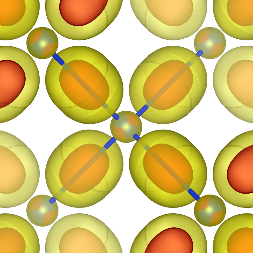
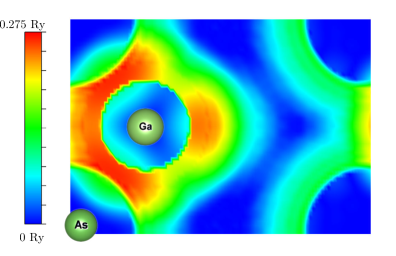
We start by mentioning that how to apply the DFT–1/2 method to the group IV semiconductors C, Si, and Ge is unclear. In contrast to binary compounds, the self-energy correction potential has not always been calculated from 1/2-ionized free atoms, but from 1/4-ionized ones [i.e., with in the second term of Eq. (6)]. Actually, for diamond was calculated in Refs. Ferreira et al., 2008, 2011 by ionizing both the – and –bands by a 1/4-electron charge (in total, removing half an electron), whereas for Si and Ge only the –band receives a 1/4-ionization correction. The argument behind this is that the orbital at the VBM overlaps with the correction potential of both atoms in the unit cell, such that only a 1/4 electron should be removed on each atom to avoid a correction that is too large. This is illustrated for Si in Fig. 1, where we can see that is the largest at the Si–Si bond center.
Turning to our DFT–1/2 calculations, Table 1 shows the results for a set of covalent semiconductors that were obtained with a 1/2- or 1/4-ionization correction. Furthermore, both LDA and PBE were considered for the underlying semilocal functional. All atoms were corrected and the ionized orbital is the one with the largest contribution to the VBM. For SiC and AlP, an additional calculation was done where the correction is applied only to the anion.
Indeed, we can see that the band gaps obtained using a 1/4-ionization correction (i.e., LDA–1/4 and PBE–1/4) are very accurate for Si and SiC, since the values differ by at most compared to experiment, while using a 1/2-ionization correction (i.e., LDA–1/2 and PBE–1/2) leads to overestimations of at least . For diamond, the results show that using a 1/2-ionized (1/4-ionized) correction leads to an overestimation (underestimation) of about . For Ge, the experimental gap of lies above the LDA–1/2 and PBE–1/2 values by about 0.4 and , respectively, while using a 1/4-ionized correction leads to strongly underestimated values. Note the contrast between Si and Ge which require different ionization, despite having relatively similar valence band density and optimized cutoff radius in Eq. (7).
Another issue that may arise is the ambiguity in choosing the atom(s) and/or orbital(s) on which the correction should be applied. For instance in the case of binary semiconductors, it has been claimedFerreira et al. (2008) that in most cases (but not always) only the correction on the anion has an impact on the results. While this may be true for ionic solids, where the states at the VBM come only from the anion, such choice can not be always justified in the case of binary semiconductors where both atoms may contribute to the VBM. Thus, in addition to the degree of ionization correction (e.g., 1/4 or 1/2), it may not be always clear on which atoms the potential should be applied. Since in SiC the VBM has a dominant –orbital character from the C atom, we did an alternative calculation where the correction is applied only to the C atom. Compared to the usual procedure where the orbitals on all atoms are corrected, a reduction of the band gap by is observed. Good agreement with experiment is obtained with 1/4-ionized correction (even though there is very little correction potential overlap at the VBM in this case), while a 1/2-ionized correction leads to large overestimations of similar to Si.
Considering the III–V compounds, we see that LDA–1/2 and PBE–1/2 clearly overestimate the band gaps for the B and Al compounds, while a moderate overestimation is observed for GaN and GaP. On the other hand, PBE–1/2 performs very well for GaAs and GaSb since the error is below .
On average, PBE–1/4 is the most accurate of the DFT–1/2 methods for this test set. It provides in eight cases the best agreement with experiment and leads to a MAE of only ; this is half of the one for PBE–1/2 () which is the worst of the DFT–1/2 methods. However, note that the mBJ potential which has MAE of and MARE of 7% is clearly more accurate. In comparison, LDA and PBE lead to MAE that are around . The general observation is that a 1/4 ionization is more appropriate for the light systems, but not sufficient for the heavier ones, i.e., those with Ga or Ge atoms, for which a 1/2-ionization correction, either with LDA or PBE, is usually more suitable. Nevertheless, a few borderline cases are C, BN, and GaP, where the best correction also depends on the underlying semilocal functional. We also mention that for only one system (GaN), there is no overlap (loosely defined as whether the sum of the cutoff radii of two nearest-neighboring atoms is larger than their distance) between the correction potentials , while for the other Ga compounds the overlap is small (tenths of one , compared to an overlap of in Si and Ge).
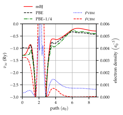
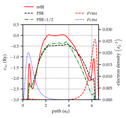
In Fig. 2, the exchange–correlation potentials mBJ, PBE, and PBE–1/4 in Si are compared. The band gaps from mBJ () and PBE–1/4 () are relatively close to each other, but the corresponding potentials show noticeable differences. Compared to PBE, PBE–1/4 corrects the band gap by lowering the energy in the region where the VBM density is very large (in the region within from the atom), whereas mBJ has a smaller correction. On the other hand, at the CBM mBJ leads to a larger up-shift than PBE–1/4.
Concerning the orbital to which the ionization should be applied, the Ga compounds are interesting since they are not always treated the same way. For some reported calculations,Ferreira et al. (2008); Pelá et al. (2012) the –orbital was ionized for all Ga compounds, while in Ref. Ribeiro et al., 2011, the Ga –orbital in GaAs was ionized as deduced from a partial charge analysis at the VBM.
In order to find which orbital should be corrected, we used the new pes module in WIEN2k.Bagheri and Blaha (2019) Using this module, we can decompose the interstital charge into their atomic orbital contributions and get atomic partial charges uniquely and independently on the choice of the atomic sphere radii and the localization of different orbitals. For instance in GaN only of the Ga-4 charge, but of Ga-3 charge are enclosed inside the atomic sphere, and thus the Ga-3 charge dominates over Ga-4 when considering the charges within the atomic sphere. However, the rescaled orbital character contributions at the VBM are and of Ga-4 and Ga-3, respectively, and of N-2. For the heavier Ga compounds, we find progressively larger Ga- and smaller Ga- character contributions at the VBM. Thus, that means that a proper ionization correction for the Ga compounds should be applied to the Ga-4 orbital.
The comparison of our calculations to those found in literature needs to be done carefully, because the correction potential is not always calculated the same way (e.g., 1/2- or 1/4-ionization and on which atoms) and, furthermore, the details are not always specified. For instance, our LDA–1/4 result for Si agrees perfectly with the one from Ferreira et al. (2008) while in this same work C was corrected with a 1/4-ionization for both – and –orbitals, leading to a value of that differs substantially from our result even when we use the same ionization scheme (, which is very close to with LDA–1/2). This discrepancy for C is unclear.
The comparison with the results from the recent implementation of the DFT–1/2 method in the LAPW exciting codePela et al. (2017) shows perfect agreement, but it also shows the importance of knowing the exact correction procedure, since for AlP the agreement is obtained if the correction is applied only to the P atom, although we cannot be sure that this scheme was used in Ref. Pela et al., 2017. However, for GaN and GaAs our results in Table 1 (without spin-orbit coupling for GaAs) show that agreement with those of Pela et al. (2017) is only obtained if the Ga –orbitals (and not the –orbitals) and N/As –orbitals are corrected, although in GaAs the Ga –orbital contributes non-negligibly to the VBM. Thus, these examples show that for a meaningful comparison of results of two sets of DFT–1/2 calculations, one needs to know the details of the calculations, since depending on the ionization correction (1/4 or 1/2) and on which atoms/orbitals it is applied, a sizeable variation in the results can be obtained.
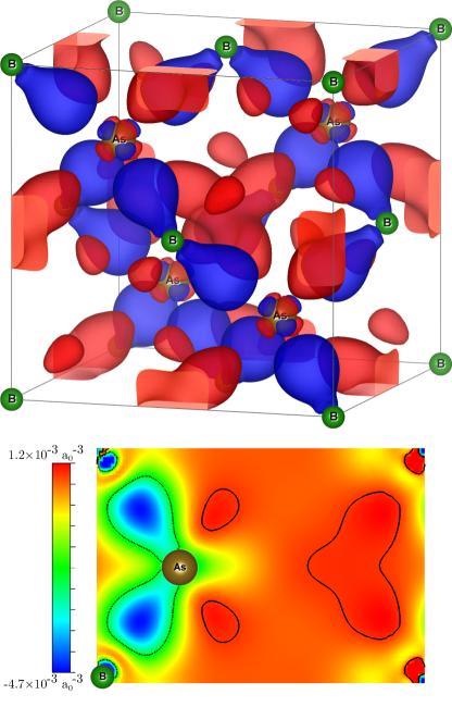
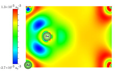
In general, a more valid explanation for some of the overestimations found in covalent materials is that these are not necessarily due to overlapping holes, but simply due to the fact that the assumptions used in deriving the method (see Sec. II) may be too crude. The larger the difference between the VBM density and the corresponding atomic density (from which the self-correction potential is calculated) is, the worse the DFT–1/2 method should perform. This is illustrated with the case of BAs, where even the 1/4-ionization correction clearly overestimates the experimental band gap. The VBM in BAs has very little pure atomic character, but is strongly hybridized and thus very aspherical, as seen on Fig. 3. The asphericity in the valence distribution causes an overestimation of the band gap, because the matrix element of [Eq. (5)] will be too large when the charge distribution is spread out compared to the non-hybridized atomic case. In many cases, this will also cause an overlap, but not always (see for example BeTe below).
III.2 Be compounds
| Solid | LDA | LDA–1/4 | LDA–1/2 | PBE | PBE–1/4 | PBE–1/2 | mBJ | Expt. | ||
|---|---|---|---|---|---|---|---|---|---|---|
| BeO | 0.00, 2.52 | 7.49 | 8.71 | 10.05 | 7.57 | 8.88 | 10.32 | 9.58 | 10.60 | |
| BeS | 0.44, 3.28 | 2.92 | 3.74 | 4.60 | 3.13 | 4.01 | 4.94 | 4.13 | 4.92 | |
| BeSe | 0.48, 3.44 | 2.34 | 3.14 | 4.00 | 2.51 | 3.36 | 4.26 | 3.39 | 4.19 | 4.0–4.5 |
| BeTe | 0.33, 3.79 | 1.57 | 2.25 | 2.97 | 1.69 | 2.41 | 3.17 | 2.33 | 2.7 |
An interesting case study for the DFT–1/2 method that has not been considered previously consists of the Be compounds BeO, BeS, BeSe, and BeTe, where the first one has the wurtzite structure, while the others have the zincblende structure. We chose these compounds to investigate the behavior of DFT–1/2 because of the descending order of ionicity along the series. The results for the band gap can be found in Table 2 where we can see that the standard 1/2-ionization correction is the most effective for the first three compounds. PBE–1/2, for instance, yields a band gap of for BeO, which is within a few percent of the experimental value of , and band gaps for BeS () and BeSe () that coincide with results. For BeTe, the PBE–1/2 value is too large by , while the errors of with PBE–1/4 and LDA–1/2 are somewhat smaller.
In order to investigate the difference between, e.g., BeSe and BeTe, we now consider the PBE and PBE–1/2 band structures as well as the electron density close to the Fermi energy. The band structures for both compounds (see Fig. 4) show a very similar change when the 1/2-ionization correction is applied. Compared to PBE, the gap separating the valence and conduction bands is larger and the bands are more flat. The shift of the bands is not uniform, but no dramatic change in the shape of the bands is induced.
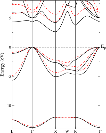
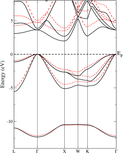
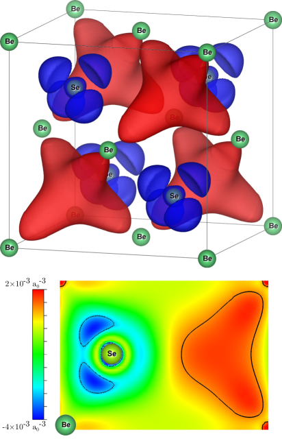
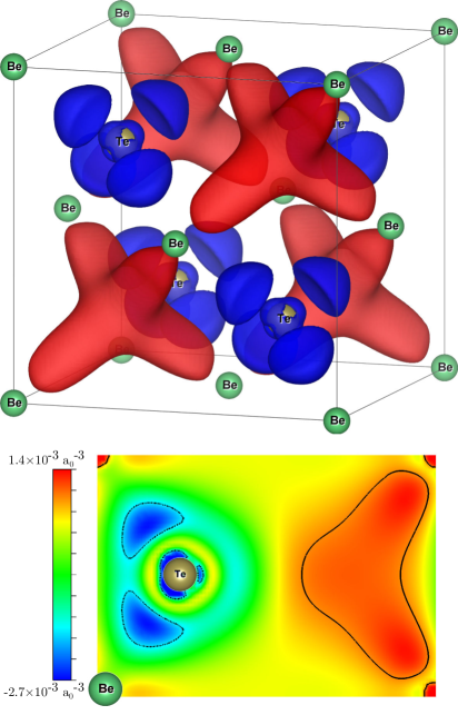
Figure 5 shows plots of electron density difference between the VBM and the CBM that are calculated in a small energy range above the CBM and below the VBM respectively, while ensuring that the total charge in both cases is equal. Two isosurfaces are shown; one in red with a positive sign (corresponding to the CBM) and one in blue (corresponding to the VBM). In the case of the Be compounds this is almost equivalent to simply superposing both densities in different colors, because both are well separated spatially (which is not always true, see Sec. III.3 below). The main observation is that there are no distinctive features that could be used to clearly judge a priori which correction (1/2 or 1/4) would be most suitable. Moreover, in both cases the valence density is mostly distributed around the anion. This is reflected in the values of the cutoff radii of Be, which in both cases is optimized to very small values (see Table 2), such that the correction potential on the cation is therefore negligible. Thus, in the case of BeTe, overlapping holes can not explain the overestimation of the band gap in PBE–1/2. Also, a partial charge analysis (again using the pes module) of the VBM reveals a nearly identical atomic –orbital character of the anion in BeSe and BeTe of and , respectively.
III.3 Transition-metal oxides
| Solid | LDA | LDA–1/2 | PBE | PBE–1/2 | mBJ | Expt. | |
|---|---|---|---|---|---|---|---|
| TiO2 | 0.29, 2.76 | 1.80 | 3.16 | 1.89 | 3.38 | 2.56 | 3.30 |
| VO2 | metal | metal | metal | metal | 0.51 | 0.6 | |
| Cu2O | 2.73, 2.21 | 0.53 | 1.09 | 0.53 | 1.14 | 0.82 | 2.17 |
| ZnO | 1.68, 2.80 | 0.74 | 3.26 | 0.81 | 3.50 | 2.65 | 3.44 |
| Cr2O3 (AFM) | 0.24, 2.0 | 1.20 | 1.35 | 1.64 | 1.76 | 3.68 | 3.4 |
| MnO (AFM) | 1.44, 2.90 | 0.74 | 1.89 | 0.89 | 2.33 | 2.94 | 3.9 |
| FeO (AFM) | metal | metal | metal | metal | 1.84 | 2.4 | |
| Fe2O3 (AFM) | 0.35, 2.87 | 0.33 | 1.33 | 0.56 | 1.66 | 2.35 | 2.2 |
| CoO (AFM) | 1.72, 2.57 | metal | metal | metal | 0.17 | 3.13 | 2.5 |
| NiO (AFM) | 1.35, 2.17 | 0.43 | 0.66 | 0.95 | 1.33 | 4.14 | 4.3 |
| CuO (AFM) | 5.42, 2.10 | metal | 0.84 | 0.06 | 1.17 | 2.27 | 1.44 |
Another class of materials that provides a challenge for the DFT–1/2 method are TM oxides. Results for some representative nonmagnetic and AFM cases are shown in Table 3. For all TM oxides the correction is based on a 1/2-ionization of the TM atom –orbital and O –orbital. For the AFM systems the self-energy correction potential is spin-dependent (and respects the AFM ordering) and calculated from a 1/2-ionization of the spin with the largest contribution to the VBM.
From the results we can see that the DFT–1/2 band gaps for the nonmagnetic TiO2 and ZnO are much larger than LDA/PBE and very close to experiment (errors are below ). However, for all other systems the band gaps calculated using DFT–1/2 are still much smaller than experiment. Actually, the DFT–1/2 method works very well for TiO2 and ZnO since these two systems have a charge-transfer band gap and thus a clear spatial separation between the VBM and CBM. This is not the case for the other systems (Cu2O, VO2, and the AFM strongly correlated systems), where a significant –character is present in both the VBM and CBM, such that the spherical atomic self-energy correction can not really distinguish these split bands; any correction that is applied to the VBM will also influence the energy level of the CBM in a similar way and thus fails to increase the band gap as much as one would like. It is well known that the standard (semi)local functionals like PBE are not able to describe strongly correlated systems properly even at the qualitative level,Terakura et al. (1984) and only more advanced methods like DFT+, hybrid functionals, or mBJ lead can lead to reasonable results. Anisimov et al. (1991); Tran et al. (2006); Marsman et al. (2008); Tran et al. (2018); Gerosa et al. (2018) Note, however, that although mBJ performs better than DFT–1/2 overall, it fails for some cases, notably TiO2, Cu2O, and ZnO (see Table 3 and Ref. Koller et al., 2011).
In more detail, for MnO, Fe2O3, and CuO, DFT–1/2 leads to a clear (but not sufficient) improvement of at least in the band gap, which is, however, not as impressive as in TiO2 and ZnO. This has to be compared to the small improvement of a few tenths of an eV obtained for NiO and Cr2O3 and the metallic character that persists for FeO, CoO, and VO2. Actually, the common feature of Fe2O3, MnO, and CuO is to have CBM and VBM that are made of states of opposite spins, as a consequence of the large exchange splitting.Terakura et al. (1984) Since the correction potential is spin-dependent (the ionization is done for the spin with the largest contribution to the VBM), a sizeable increase in the band gap is possible. In other TM oxides like NiO, FeO, or CoO the crystal field splitting is dominant, such that the VBM has a more mixed spin population.
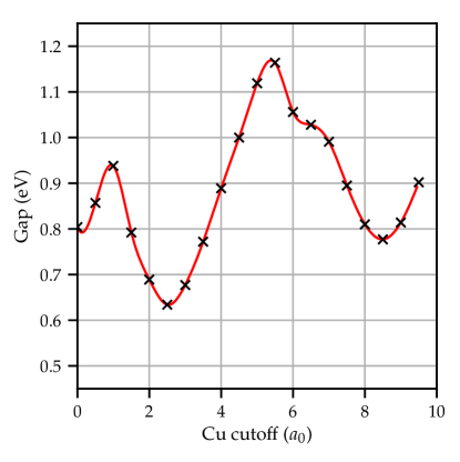
In CuO, the choice for the spin for calculating the potential is crucial. The calculation done with the ionization correction applied to the correct spin (i.e. the one which has the largest population at the VBM for the given atom) gives a PBE–1/2 result of , whereas calculating using the other spin results in a band gap of only . Another particular feature of CuO is the cutoff radius of the Cu atom, which is extremely large (). As shown in Ref. Xue et al., 2018, the band gap as a function of may consist of several maxima when reaches the next coordination shell. Usually, one would expect the global maximum of the band gap with respect to to be at the first maximum (see Ref. Xue et al., 2018), however, as shown in Fig. 6 the second maximum at is higher than the first one at about . Note that is very close to the distance to the nearest Cu atom of , which means an overlap with a large portion of the neighboring Cu –orbitals. Such overlap introduces a small anisotropy in the superimposed correction potential around each Cu atom. We mention that because of numerical problems in the calculations when cutoff radii larger than are used, we could not verify whether the third local maximum would be even higher or not.
Interestingly, in Fe2O3 the reverse is observed. A slightly larger band gap ( with PBE–1/2) is obtained when the wrong spin is ionized for calculating the correction potential. We hypothesize that this behavior is caused by a larger bonding-antibonding splitting of the Fe-O- interaction when the wrong spin is chosen.
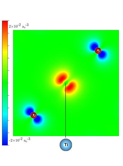
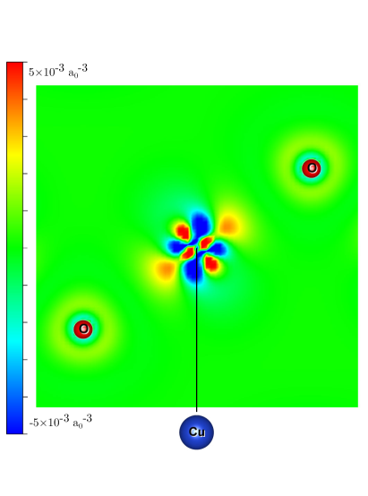
Now, a comparison between TiO2 (accurately described by DFT–1/2) and Cu2O (inaccurately described by DFT–1/2) is made. Figure 7 shows difference density plots, where the density around the VBM is subtracted from the one around the CBM. In TiO2 the VBM and CBM are, as expected, spatially well separated with the conduction band consisting primarily of the Ti –orbitals and the valence band of the O –orbitals. In Cu2O, however, both bands are predominantly composed of Cu –orbitals, i.e., the –orbitals are split across the Fermi level due to the crystal field. The conduction band (in red) has a strong character with lobes pointing towards the O atom, while the lobes of the valence band (in blue) point in other directions. Thus, as clearly visible, in Cu2O the VBM and CBM are located on the same atom such that the spherical correction potential can barely increase the energy difference between the VBM and CBM.
The PBE and PBE–1/2 band structures of TiO2 and Cu2O are shown in Figs. 8(a) and 8(b), respectively. For TiO2, the band gap is approximately twice as large. Changes in the shape of the bands are rather minor for the conduction bands, but more pronounced differences can be observed in the occupied bands, e.g., at the and R points in the range 4 – below the Fermi energy, where the changes do not consist of a simple shift. Among the differences in the shape of the bands in Cu2O, there is for instance the crossing of bands at at with PBE, while they are clearly separated with PBE–1/2. The band that is significantly raised in energy has a strong Cu –character, whereas the bands that are not shifted relative to the Fermi energy have strong O –character.
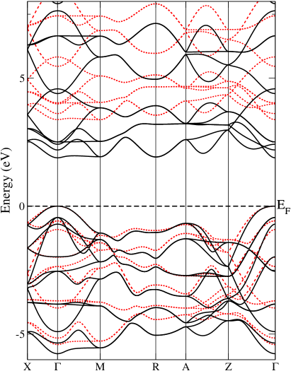
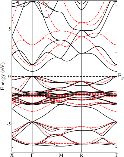
Figure 9 shows the mBJ, PBE, and PBE–1/2 exchange–correlation potentials in TiO2, which lead to band gaps of , , and , respectively. As mentioned above, mBJ performs badly. We can see that compared to PBE, mBJ raises the energy in the interstitial and has peaks at the outer atomic orbitals for both Ti and O (where respectively the CBM and VBM have a large density). With PBE–1/2 a much more accurate band gap is achieved thanks to a significantly more negative potential at the VBM region around the O atom.
To finish, we mention that Xue et al. (2018) reported a similar issue in Li2O2 as in Cu2O. In this case the O –bands are split across the Fermi level, with the VBM formed by the (degenerate) and –orbitals and the CBM by the –band, while the correction potential is calculated from an atomic calculation, which is spherically symmetric. Thus, as in Ref. Xue et al., 2018, a severe underestimation of the band gap for Li2O2 is obtained and our LDA–1/2 and PBE–1/2 values are 2.52 and , respectively (only larger than LDA and PBE), while experiment is . With a value of , the mBJ potential succeeds in describing the band gap very accurately.
III.4 Shell correction for DFT–1/2
Xue et al. (2018) proposed a more general version of DFT–1/2, called shDFT–1/2 (sh is a shorthand for shell), which employs a modified, shell-like cutoff function
| (8) |
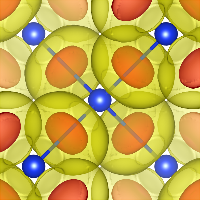
with two variationally determined parameters and and a sharper cutoff compared to Eq. (7). Note that the shell-like cutoff function reduces to the spherical one of Eq. (7) when the inner radius is chosen as , but with an exponent of 20 instead of 8. The inner radius is also used to maximize the band gap, which implies that the band gap calculated with shDFT–1/2 should be larger compared to optimizing only as done with DFT–1/2. The aim of introducing an inner radius is to avoid unwanted interaction of (semi-)core electrons with the correction potential . However, optimizing the radii in the shDFT–1/2 method is more tedious, since and need to be optimized simultaneously and may be interdependent. For example in GaAs, DFT–1/2 requires a Ga cutoff of ,Ferreira et al. (2008) whereas shLDA–1/4 requires , and Xue et al. (2018) for the same atom. In this case (as in some others) the correction potential of both atoms overlap with the valence density that is distributed around one of the atoms as illustrated in Fig. 10 for GaAs. However, a well-founded explanation why this approach should yield more accurate band gaps is not provided in Ref. Xue et al., 2018.
| Solid | Eq. (7) | Eq. (8) |
|---|---|---|
| Ge–1/4 | 0.27 | 0.41 |
| AlP–0–1/2 | 3.21 | 3.33 |
| BN–0–1/2 | 6.79 | 6.97 |
| BeSe–0–1/2 | 4.26 | 4.40 |
| GaAs–1/4 | 0.97 | 1.06 |
| Solid | PBE | PBE–1/4 | PBE–0–1/2 | shPBE–1/4 | shPBE–0–1/2 | Expt. | ||
|---|---|---|---|---|---|---|---|---|
| Ge | 1.71 | 3.30 | metal | 0.27 | 0.59 | 0.93111Obtained with the preferred correction according to Xue et al. (2018) | 1.78 | 0.74 |
| SiC | 0.12 | 2.61 | 1.35 | 2.43 | 3.31 | 2.55 | 3.52111Obtained with the preferred correction according to Xue et al. (2018) | 2.42 |
| BN | 0.15 | 2.14 | 4.47 | 5.79 | 6.79 | 5.87 | 7.03111Obtained with the preferred correction according to Xue et al. (2018) | 6.36 |
| BAs | 0.18, 0.89 | 2.81, 2.70 | 1.09 | 1.93 | 2.00 | 2.03 | 2.14 | 1.46 |
| AlN | 0.13 | 2.51 | 3.34 | 4.66 | 5.96 | 4.78 | 6.19 | 4.90 |
| AlP | 0.66 | 3.15 | 1.59 | 2.50 | 3.21 | 2.59 | 3.36111Obtained with the preferred correction according to Xue et al. (2018) | 2.5 |
| GaN | 0.16 | 2.53 | 1.66 | 2.55 | 3.41 | 2.71 | 3.55111Obtained with the preferred correction according to Xue et al. (2018) | 3.28 |
| GaAs | 2.17, 1.48 | 4.21, 3.25 | 0.43 | 0.97 | 1.49 | 1.54111Obtained with the preferred correction according to Xue et al. (2018) | 2.04 | 1.52 |
| BeSe | 0.83 | 2.89 | 2.51 | 3.36 | 4.26 | 3.55 | 4.44111Obtained with the preferred correction according to Xue et al. (2018) | 4.0-4.5 |
| BeTe | 1.15 | 3.22 | 1.69 | 2.41 | 3.17 | 2.69 | 3.42111Obtained with the preferred correction according to Xue et al. (2018) | 2.7 |
| ZnO | 0.13, 0.10 | 1.43, 2.38 | 0.81 | 2.08 | 2.32 | 2.21 | 2.36111Obtained with the preferred correction according to Xue et al. (2018) | 3.44 |
| NiO | -0.25, 0.12 | 1.29, 1.25 | 0.95 | metal | 1.33 | metal | 1.36111Obtained with the preferred correction according to Xue et al. (2018) | 4.3 |
Xue et al. (2018) also prescribed a procedure to choose the correction. In monoatomic compounds, there is a choice to apply either a 1/2- or a 1/4-ionization correction. The former should be used when the VBM density is distributed around the atom (like in diamond), while the latter should be used when the VBM density is distributed around the bond center (like in Si, see Sec. III.1). In binary compounds, either a 1/2-ionization correction is applied to the anion or a 1/4 ionization to both the anion and cation. Which one of these two corrections is applied depends on the CBM density distribution. When the CBM density is distributed close to the cation-cation bonds (AlP is the example given by Xue et al. (2018), but this would apply also to BeSe and BeTe, see Fig. 5), only the anion should be corrected by a 1/2-ionization. However, when the CBM density is distributed around the atoms, like in GaAs (Fig. 10), a 1/4-ionization correction should be applied to both atoms, and in such a case a large should minimize the interaction of the correction potential with the CBM. However, how to deal with a case like ZnO where a 1/2-ionization correction on both atoms is needed to obtain a reasonable band gap Ferreira et al. (2011) is not discussed. It is also clear that other situations exist, like BAs (see Fig. 3) where the CBM density is distributed along the cation bonds but also around the anion (note the CBM lobes around the As atom, which are absent in BeSe and BeTe, see Fig. 5).
Before discussing the results obtained with shPBE–1/2, the influence of the steepness of the outer part of Eq. (8) is now discussed. As noted above, the outer cutoff is sharper in the shell function [Eq. (8)] than in the original spherical function [Eq. (7)]. In order to test the influence of the outer steepness on the results, calculations with Eq. (8) were done using no inner cutoff (i.e., with , see discussion above) and the results are compared to those obtained with Eq. (7). The band gaps obtained with the two cutoff functions are shown in Table 4, where we can see that Eq. (8) leads to values that are moderately larger by . This is easily explained by noting that a steeper cutoff can more effectively maximize (minimize) the overlap of with the VBM (CBM).
Representative compounds were considered for calculations with the shDFT–1/2 method. We chose border cases (BeTe and BeSe), some of the group IV and III-V semiconductors whose band gaps are significantly underestimated in a 1/4-ionization correction, and BAs to check if the overestimation found even in LDA–1/4 is worsened or not. We also included one nonmagnetic (ZnO) and one AFM TM oxide (NiO) to see the influence of the inner cutoff on this class of materials. We limited our calculations to the PBE functional.
The results obtained with the shPBE–1/2 methods are shown in Table 5. Compared to the corresponding PBE–1/2 methods with the same ionization correction, the improvement is in most cases rather small or non-existent. Actually, comparing the results to those from Table 4 discussed above, in most cases (e.g., AlP, BN, or BeSe) the increase in the band gap is mostly due to the sharper cutoff and not to the inner radius . It is only for Ge and GaAs that the inner radius has a large influence on the results. For these two latter cases, excellent agreement with experiment is obtained with shPBE–1/4. The other main observation is that shPBE-0-1/2 (1/2-ionization correction applied only to the anion) strongly overestimates the band gap in all cases except ZnO and NiO. In the case of NiO, it is expected since also the shell correction can not capture the – transition that makes up the fundamental gap. The case of ZnO shows that sometimes a 1/2-ionization correction on both atoms is required to obtain a good band gap (see Table 3).
Actually, with the larger set of solids used by Xue et al. (2018) to test shLDA–1/2, the overall improvement is rather modest, in particular when taking account the fact that an extra parameter () is introduced and leads to a more cumbersome procedure.
IV Summary
Since the DFT–1/2 method has been proposed, a large number of works reporting accurate results for the band gap have been published. However, as discussed in Xue et al. (2018) and in the present work, the method has flaws which prevent its straightforward application. Firstly, for the cases where the states around the band gap, i.e., both at the VBM and CBM, come from orbitals centered at the same atom, the method will most likely fail. Such examples discussed in this work are many TM oxides, but also Li2O2.
Secondly, the method can not be blindly applied to covalent semiconductors and it is only recentlyXue et al. (2018) that this discussion has been extended beyond the group IV semiconductors. It is rather clear that there is no unique way (1/2- or 1/4-ionization correction, which atoms, and which orbital) to calculate reliably the band gap for these materials using (sh)DFT–1/2, without prior knowledge of the experimental band gap.
The comparison with the mBJ potential shows that mBJ is superior to DFT–1/2 on average. The most visible differences in the performance of DFT–1/2 and mBJ are for the TM oxides. While DFT–1/2 is very accurate for TiO2 and ZnO, but very inaccurate for the AFM oxides, the reverse is observed with mBJ.
We also considered the shell correction (shDFT–1/2). It requires the introduction of an extra parameter, which leads to a more tedious application of the method. Furthermore, it is only for a few cases that shDFT–1/2 clearly improves the results.
Thus, we conclude that while DFT–1/2 is a computationally fast method and can be accurate for band gap calculations, one should be careful in its application. In particular, the method can be applied efficiently only when the VBM and CBM are spatially well separated, like in ionic solids, such that predominantly the VBM is shifted down by the correction potential, and not the CBM. When these conditions are met, DFT–1/2 is certainly useful especially in systems with large unit cells, like for example for the calculations of defect levels,Lucatto et al. (2017); Matusalem et al. (2013) surfaces,Belabbes et al. (2011) or interfaces.Ribeiro et al. (2011, 2009) An interesting perspective opened by the DFT–1/2 technique is the semi-empirical application to larger structures. One can fit or tune the correction to a reference (e.g. bulk) configuration by parametrizing either the ionization level, or the correction factor (multiplying the correction potential by a constant factor)Ataide et al. (2017); Ribeiro (2015b) and consequently applying this semi-empirical correction in the structure of interest, e.g. defects, interfaces or surfaces.
Acknowledgements.
This work was supported by projects F41 (SFB ViCoM), W1243 (Solids4Fun), and P27738-N28 of the Austrian Science Fund (FWF).References
- Hohenberg and Kohn (1964) P. Hohenberg and W. Kohn, Phys. Rev. 136, B864 (1964).
- Kohn and Sham (1965) W. Kohn and L. J. Sham, Physical Review 140, A1133 (1965).
- Perdew (2009) J. P. Perdew, International Journal of Quantum Chemistry 28, 497 (2009).
- Perdew et al. (1996) J. P. Perdew, K. Burke, and M. Ernzerhof, Phys. Rev. Lett. 77, 3865 (1996), 78, 1396(E) (1997).
- Heyd et al. (2005) J. Heyd, J. E. Peralta, G. E. Scuseria, and R. L. Martin, J. Chem. Phys. 123, 174101 (2005).
- Aryasetiawan and Gunnarsson (1998) F. Aryasetiawan and O. Gunnarsson, Rep. Prog. Phys. 61, 237 (1998).
- Hedin (1999) L. Hedin, J. Phys.: Condens. Matter 11, R489 (1999).
- Shishkin et al. (2007) M. Shishkin, M. Marsman, and G. Kresse, Phys. Rev. Lett. 99, 246403 (2007).
- Seidl et al. (1996) A. Seidl, A. Görling, P. Vogl, J. A. Majewski, and M. Levy, Physical Review B 53, 3764 (1996).
- Becke (1993) A. D. Becke, J. Chem. Phys. 98, 5648 (1993).
- Della Sala et al. (2016) F. Della Sala, E. Fabiano, and L. A. Constantin, Int. J. Quantum Chem. 116, 1641 (2016).
- Xiao et al. (2013) B. Xiao, J. Sun, A. Ruzsinszky, J. Feng, R. Haunschild, G. E. Scuseria, and J. P. Perdew, Phys. Rev. B 88, 184103 (2013).
- Yang et al. (2016) Z.-h. Yang, H. Peng, J. Sun, and J. P. Perdew, Phys. Rev. B 93, 205205 (2016).
- Jana et al. (2018) S. Jana, A. Patra, and P. Samal, J. Chem. Phys. 149, 044120 (2018).
- Armiento and Kümmel (2013) R. Armiento and S. Kümmel, Phys. Rev. Lett. 111, 036402 (2013).
- Vlček et al. (2015) V. Vlček, G. Steinle-Neumann, L. Leppert, R. Armiento, and S. Kümmel, Phys. Rev. B 91, 035107 (2015).
- Gritsenko et al. (1995) O. Gritsenko, R. van Leeuwen, E. van Lenthe, and E. J. Baerends, Phys. Rev. A 51, 1944 (1995).
- Kuisma et al. (2010) M. Kuisma, J. Ojanen, J. Enkovaara, and T. T. Rantala, Phys. Rev. B 82, 115106 (2010).
- Tran and Blaha (2009) F. Tran and P. Blaha, Phys. Rev. Lett. 102, 226401 (2009).
- Ferreira et al. (2008) L. G. Ferreira, M. Marques, and L. K. Teles, Phys. Rev. B 78, 125116 (2008).
- Slater (1972) J. C. Slater, in Advances in Quantum Chemistry, Vol. 6 (Elsevier, 1972) pp. 1–92.
- Slater and Johnson (1972) J. C. Slater and K. H. Johnson, Phys. Rev. B 5, 844 (1972).
- Ferreira et al. (2013) L. G. Ferreira, R. R. Pelá, L. K. Teles, M. Marques, M. Ribeiro Jr., and J. Furthmüller, AIP Conference Proceedings 1566, 27 (2013).
- Ferreira et al. (2011) L. G. Ferreira, M. Marques, and L. K. Teles, AIP Advances 1, 032119 (2011).
- Pela et al. (2017) R. R. Pela, A. Gulans, and C. Draxl, Computer Physics Communications 220, 263 (2017).
- Pela et al. (2016) R. R. Pela, U. Werner, D. Nabok, and C. Draxl, Phys. Rev. B 94, 235141 (2016).
- Tao et al. (2017) S. X. Tao, X. Cao, and P. A. Bobbert, Scientific Reports 7, 14386 (2017).
- Lucatto et al. (2017) B. Lucatto, L. V. C. Assali, R. R. Pela, M. Marques, and L. K. Teles, Phys. Rev. B 96, 075145 (2017).
- Ribeiro (2015a) M. Ribeiro, Canadian Journal of Physics 93, 261 (2015a).
- Belabbes et al. (2010) A. Belabbes, A. Zaoui, and M. Ferhat, Applied Physics Letters 97, 242509 (2010).
- Santos et al. (2012) J. P. T. Santos, M. Marques, L. G. Ferreira, R. R. Pelá, and L. K. Teles, Applied Physics Letters 101, 112403 (2012).
- Ribeiro et al. (2012) M. Ribeiro, L. R. C. Fonseca, T. Sadowski, and R. Ramprasad, Journal of Applied Physics 111, 073708 (2012).
- Belabbes et al. (2011) A. Belabbes, J. Furthmüller, and F. Bechstedt, Phys. Rev. B 84, 205304 (2011).
- Küfner et al. (2012) S. Küfner, A. Schleife, B. Höffling, and F. Bechstedt, Phys. Rev. B 86, 075320 (2012).
- Ribeiro et al. (2011) M. Ribeiro, L. R. C. Fonseca, and L. G. Ferreira, EPL (Europhysics Letters) 94, 27001 (2011).
- Ribeiro et al. (2009) M. Ribeiro, L. R. C. Fonseca, and L. G. Ferreira, Phys. Rev. B 79, 241312 (2009).
- Pela et al. (2015) R. R. Pela, M. Marques, and L. K. Teles, Journal of Physics: Condensed Matter 27, 505502 (2015).
- Matusalem et al. (2018) F. Matusalem, M. Marques, L. K. Teles, A. Filippetti, and G. Cappellini, Journal of Physics: Condensed Matter 30, 365501 (2018).
- Pelá et al. (2012) R. R. Pelá, M. Marques, L. G. Ferreira, J. Furthmüller, and L. K. Teles, Applied Physics Letters 100, 202408 (2012).
- Pela et al. (2018) R. R. Pela, A. Gulans, and C. Draxl, Journal of Chemical Theory and Computation 14, 4678 (2018).
- Xue et al. (2018) K.-H. Xue, J.-H. Yuan, L. R. Fonseca, and X.-S. Miao, Computational Materials Science 153, 493 (2018).
- Perdew and Levy (1983) J. P. Perdew and M. Levy, Physical Review Letters 51, 1884 (1983).
- Yang et al. (2012) W. Yang, A. J. Cohen, and P. Mori-Sánchez, The Journal of Chemical Physics 136, 204111 (2012).
- Andrade and Aspuru-Guzik (2011) X. Andrade and A. Aspuru-Guzik, Phys. Rev. Lett. 107, 183002 (2011).
- Chai and Chen (2013) J.-D. Chai and P.-T. Chen, Phys. Rev. Lett. 110, 033002 (2013).
- Kraisler and Kronik (2014) E. Kraisler and L. Kronik, J. Chem. Phys. 140, 18A540 (2014).
- Grüning et al. (2006) M. Grüning, A. Marini, and A. Rubio, J. Chem. Phys. 124, 154108 (2006).
- Grüning et al. (2006) M. Grüning, A. Marini, and A. Rubio, Phys. Rev. B 74, 161103(R) (2006).
- Janak (1978) J. F. Janak, Phys. Rev. B 18, 7165 (1978).
- Kümmel and Kronik (2008) S. Kümmel and L. Kronik, Rev. Mod. Phys. 80, 3 (2008).
- Ataide et al. (2017) C. A. Ataide, R. R. Pelá, M. Marques, L. K. Teles, J. Furthmüller, and F. Bechstedt, Phys. Rev. B 95, 045126 (2017).
- Ribeiro (2015b) M. Ribeiro, Journal of Applied Physics 117, 234302 (2015b).
- Blaha et al. (2018) P. Blaha, K. Schwarz, G. K. H. Madsen, D. Kvasnicka, J. Luitz, R. Laskowski, F. Tran, and L. D. Marks, WIEN2k: An Augmented Plane Wave plus Local Orbitals Program for Calculating Crystal Properties (Vienna University of Technology, Austria, 2018).
- Andersen (1975) O. K. Andersen, Phys. Rev. B 12, 3060 (1975).
- Singh and Nordström (2006) D. J. Singh and L. Nordström, Planewaves, Pseudopotentials, and the LAPW Method, 2nd ed. (Springer, New York, 2006).
- (56) See Supplemental Material at http://link.aps.org/supplemental/ for the experimental lattice constants of the solids used for the calculations.
- Tran and Blaha (2017) F. Tran and P. Blaha, J. Phys. Chem. A 121, 3318 (2017).
- Tran et al. (2018) F. Tran, S. Ehsan, and P. Blaha, Phys. Rev. Materials 2, 023802 (2018).
- Lee et al. (2016a) J. Lee, A. Seko, K. Shitara, K. Nakayama, and I. Tanaka, Phys. Rev. B 93, 115104 (2016a).
- Nakano and Sakai (2018) K. Nakano and T. Sakai, J. Appl. Phys. 123, 015104 (2018).
- Lucero et al. (2012) M. J. Lucero, T. M. Henderson, and G. E. Scuseria, Journal of Physics: Condensed Matter 24, 145504 (2012).
- Crowley et al. (2016) J. M. Crowley, J. Tahir-Kheli, and W. A. Goddard, The Journal of Physical Chemistry Letters 7, 1198 (2016).
- Bagheri and Blaha (2019) M. Bagheri and P. Blaha, Journal of Electron Spectroscopy and Related Phenomena 230, 1 (2019).
- Lee et al. (2016b) J. Lee, A. Seko, K. Shitara, K. Nakayama, and I. Tanaka, Physical Review B 93, 12 (2016b).
- Yim et al. (1972) W. Yim, J. Dismukes, E. Stofko, and R. Paff, Journal of Physics and Chemistry of Solids 33, 501 (1972).
- Nagelstraßer et al. (1998) M. Nagelstraßer, H. Dröge, H.-P. Steinrück, F. Fischer, T. Litz, A. Waag, G. Landwehr, A. Fleszar, and W. Hanke, Physical Review B 58, 10394 (1998).
- Hummelshøj et al. (2010) J. S. Hummelshøj, J. Blomqvist, S. Datta, T. Vegge, J. Rossmeisl, K. S. Thygesen, A. C. Luntz, K. W. Jacobsen, and J. K. Nørskov, The Journal of Chemical Physics 132, 071101 (2010).
- Gillen and Robertson (2013) R. Gillen and J. Robertson, Journal of Physics: Condensed Matter 25, 165502 (2013).
- Wang et al. (2016) Y. Wang, S. Lany, J. Ghanbaja, Y. Fagot-Revurat, Y. P. Chen, F. Soldera, D. Horwat, F. Mücklich, and J. F. Pierson, Phys. Rev. B 94, 245418 (2016).
- Terakura et al. (1984) K. Terakura, T. Oguchi, A. R. Williams, and J. Kübler, Phys. Rev. B 30, 4734 (1984).
- Anisimov et al. (1991) V. I. Anisimov, J. Zaanen, and O. K. Andersen, Phys. Rev. B 44, 943 (1991).
- Tran et al. (2006) F. Tran, P. Blaha, K. Schwarz, and P. Novák, Phys. Rev. B 74, 155108 (2006).
- Marsman et al. (2008) M. Marsman, J. Paier, A. Stroppa, and G. Kresse, J. Phys.: Condens. Matter 20, 064201 (2008).
- Gerosa et al. (2018) M. Gerosa, C. E. Bottani, C. D. Valentin, G. Onida, and G. Pacchioni, J. Phys.: Condens. Matter 30, 044003 (2018).
- Koller et al. (2011) D. Koller, F. Tran, and P. Blaha, Phys. Rev. B 83, 195134 (2011).
- Matusalem et al. (2013) F. Matusalem, J. Ribeiro, Mauro, M. Marques, R. R. Pelá, L. G. Ferreira, and L. K. Teles, Phys. Rev. B 88, 224102 (2013).