Probing the light hole / heavy hole switching with correlated magneto-optical spectroscopy and chemical analysis on a single quantum dot
Abstract
A whole series of complementary studies have been performed on the same, single nanowire containing a quantum dot: cathodoluminescence spectroscopy and imaging, micro-photoluminescence spectroscopy under magnetic field and as a function of temperature, and energy-dispersive X-ray spectrometry and imaging. The ZnTe nanowire was deposited on a Si3N4 membrane with Ti/Al patterns. The complete set of data shows that the CdTe quantum dot features the heavy-hole state as a ground state, although the compressive mismatch strain promotes a light-hole ground state as soon as the aspect ratio is larger than unity (elongated dot). A numerical calculation of the whole structure shows that the transition from the heavy-hole to the light-hole configuration is pushed toward values of the aspect ratio much larger than unity by the presence of a (Zn,Mg)Te shell, and that the effect is further enhanced by a small valence band offset between the semiconductors in the dot and around it.
-
November 2018
Keywords: nanowires, quantum dot, semiconductors, molecular beam epitaxy, optical spectroscopy, cathodoluminescence, EDX
1 Introduction
Quantum confinement in semiconductor nanostructures is currently explored in order to achieve specific functions in the field of nanophotonics, nanoelectronics, nanomagnetism, quantum information, communication and sensing. A prerequisite is to be able to address a single object, for instance to achieve the emission of single photons or entangled photon pairs, or various realizations of qubits. Addressing and scaling constitute a clear advantage of semiconductors with respect to other systems; however there is a large dispersion from one single object to another one, up to the point that in order to reach a better understanding of the relevant physical mechanisms, it is mandatory to apply complementary experimental methods not to an ensemble nor to a collection of single objects, but all to the very same single object. Here we present and exploit a multiple-technique approach which can be applied to any system which can be physically manipulated, such as a nanowire (NW), a quantum dot (QD) in a NW, a nanocristallite, or any system where the actual configuration controls the electronic, photonic and spin properties.
The system under study is a QD in a NW. The advantage of fabricating a QD insertion in a NW is that it permits to combine a large variety of different materials and to control the size and shape of the QD over a very broad range, much broader than by using the usual Stranski-Krastanow (SK) growth mode. It is thus possible to design the aspect ratio and mismatch strain configurations, in such a way that the ground state at the top of the valence band is the light-hole state [1, 2, 3]. A proper control of the hole state has decisive consequences on many physical properties, such as the selection rules of excitons and charged excitons and the opportunity to optically manipulate the qubit formed on a confined carrier, the diagram of light emission and polarization, the spin anisotropy of a confined carrier and the corresponding dynamics, or the magnetic anisotropy in case of coupling with magnetic impurities, to cite but a few. The selection rules for an exciton associated with a light hole naturally form the so-called lambda-configuration required for the manipulation of the spin state of a confined carrier: the solution exploited so far [4] involves complex structures incorporating a ferroelectric stressor, while using a mismatched elongated QD offers a straightforward solution. By contrast, the orientation of the emitting dipole realized by a heavy hole exciton is more adapted to light guiding: the low emission efficiency of InAsP/InP QDs in NWs was attributed [5] to the use of elongated QDs in order to shift the wavelength to the telecom band (1.55 m), thus favoring a light-hole exciton. The design of the shell is also of prime importance, including tapering [5] to improve the coupling to a photonic structure or free space propagation, and an asymmetric cross section [6, 7] to drive the emission into a single linearly polarized optical mode: in all cases, the control of the shape and size of the QD and its position within a NW with a well controlled profile is needed, and we demonstrate here that the EDX tomographic approach [8] can be combined with a spectroscopic and photonic characterization. Finally, the design of the spin anisotropy of the confined carrier has many consequences: an example is the fine structure and the associated spin dynamics of the carrier contemplated as a qubit. Another interesting aspect is the magnetic anisotropy of the magnetic polaron formed in a dot made of a dilute magnetic semiconductor such as Cd1-xMnxTe. While magnetic polarons formed around a heavy-hole exciton have been studied for a long time [9], they were not yet observed in structures where light holes could be favored [10, 11]. Finally, combining chemical analysis and spectroscopy on the same nanoobject would be highly relevant in the case of colloidal nanoparticles: to stay with dilute magnetic system, we just mention II-VI nanoparticles [12, 13] and halide perovskites [14, 15].
In the simple case of a QD made of an isotropic material embedded in a thick matrix with a smaller lattice parameter, the built-in elastic strain (Eshelby model [16]) tends to link the ground state to the heavy-hole in a flat ellipsoidal QD, and to the light-hole in an elongated QD; the boundary is the spherical QD where the fourfold degeneracy is restored. The Luttinger Hamiltonian and the anisotropic elastic properties should be taken into account but both feature cubic symmetry and thus should not lift this fourfold degeneracy. However an additional shell with a different lattice parameter is often added in order to passivate the surface and it may significantly affect the position of the light-hole/heavy-hole crossover.
This is the case of the QD under study, a Cd1-xMnxTe elongated insertion embedded in a ZnTe/Zn1-yMgyTe core-shell NW: the ZnTe core has the smallest lattice parameter, so that the elongated dot favors the light hole while the outer shell tends to restore the heavy hole. Most QDs from the same sample exhibit a light-hole ground state (as demonstrated in our previous study [3]) but some exhibit a heavy-hole one. Our multiple-technique approach combines (1) high-resolution scanning transmission electron microscopy combined with energy-dispersive x-ray spectrometry (EDX) with imaging and 3D reconstruction through discrete tomography, (2) scanning electron microscopy (SEM) with low-temperature cathodoluminescence (CL) spectroscopy and imaging, and (3) micro-photoluminescence (PL) at variable temperature under applied magnetic field. All these experimental methods were applied to the same QD, placed on a dedicated micro-fabricated silicon nitride membrane using a micromanipulator. We show that this QD hosts a heavy-hole ground state in spite of its elongated shape with an aspect ratio definitely larger than unity; a calculation of the hole states by using the TBSim package of codes [17] shows that the strain induced by the shell pushes the heavy-hole / light-hole crossing to values of the aspect ratio larger than unity, the effect being enhanced if the valence band offset is small.
2 Methods
The micro-fabricated TEM grid PL sample holder is based on Si3N4 membranes, thin enough (50 nm) to be transparent to an electron beam, and compatible with low-temperature spectroscopy. The same type of membrane was used to identify the influence of crystal structure and defects on electronic properties, for instance to determine the influence of the polarity of a contacted GaN-AlN NW heterostructure on its current-voltage characteristics [18], or to associate a specific PL line to polytypes [19, 20] or polarity inversion boundaries [21]. Here we go one step further and combine a quantitative study of the morphology of a nanofabricated single object (the composition profile of a QD embedded in a NW) and the study of its electronic properties. The silicon nitride membranes were fabricated from a 300 m thick Si(100) four-inch wafer with 50 nm of stoichiometric Si3N4 deposited by LioniX International on both sides. Using laser lithography followed by a reactive ion etching step a pattern is written in the Si3N4 layer. Then a KOH bath at 80∘C etches through the Si on the other side of the wafer, leaving only the layer of Si3N4, which now constitutes the membrane. Next, markers are defined by UV laser lithography and electron beam deposition of Ti/Al (10 nm / 50 nm), followed by a lift-off step to remove the metal deposited on the resist; these markers (Fig. 1a) allow us to rapidly identify the NW all along the chain of experimental set-ups.
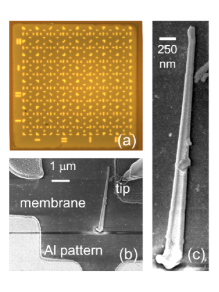
The sample was grown as described previously [22]. We used a (111)B Cd0.96Zn0.04Te substrate with a small misorientation () to avoid the formation of twins during the growth of the preliminary ZnTe buffer layer. The NW (NW S2 of our EDX study [8]) was transferred from the as-grown sample to the sample holder silicon nitride membrane, using the micromanipulator of a dual beam FIB/SEM machine (Zeiss NVision 40 DualBeam), see Fig. 1b.
The CL set-up consists of a FESEM FEI Inspect F50 to ensure a high spatial resolution (a few nm at 5 keV), with a IHR550 spectrometer equipped with a CL accessory and a low-temperature Gatan stage to cool the sample down to K. It is often convenient to perform CL as a first characterization, implying that the electron beam intensity and voltage be kept low enough, typically 250 pA and 5keV, to reduce defect formation.
The magneto-optical properties were studied using a low temperature confocal micro-PL set-up [23]. The sample holder was mounted in a helium-flow cryostat (Oxford Spectromag), with temperature between 300 K and 4.2 K, and a magnetic field up to 11 T in the Faraday configuration (excitation and detection along the magnetic field, perpendicular to the NW axis). The NW was excited by a 488 nm cw laser beam focused to 4 m2, using a 100X Mitutoyo magnification microscope and a piezoelectric scanner. Unless mentioned, the laser power was kept well below 1 W in order to minimize heating. The PL signal was collected by the same microscope objective and sent into a 0.46 m Jobin-Yvon spectrometer equipped with a CCD camera.
EDX spectrometry was performed in a FEI Tecnai Osiris S/TEM equipped with four Silicon Drift Detectors, operated at 200 keV. The EDX signal is collected as an hypermap where each pixel corresponds to the x-ray emission spectrum of atoms along the electron beam. We used the Quantax-800 software from Bruker for background correction and deconvolution, to extract the contributions of the L lines of Te, Cd, Au, and K lines of Zn, Mg, and O. A transparent sample holder must be used if the goal is a quantitative analysis of the EDX in order to extract chemical profiles, as the signal from a bulk sample holder would totally blind the detectors. If needed, it is possible to rotate the NW around its axis: discrete tomography is then achieved by recording at least 2 projections along two nearly orthogonal axes [8].
The structural and electronic properties of nanowires were calculated numerically with the TBSim code [17]. The strains are first computed with a finite elements discretization of continuous elasticity equations. The Poisson equation is then solved for the resulting piezoelectric potential. Finally, the hole states are calculated with a six-bands k.p model discretized on the same mesh. The lattice parameters, elastic, dielectric and piezoelectric constants of the materials are: 6.481 Å, 61.5 GPa, 43 GPa, 19.6 GPa, 10.6, 0.03 C m-2 for CdTe, and 6.104 Å, 71.6 GPa, 40.7 GPa, 31.2 GPa, 10.1, 0.03 C m-2 for ZnTe. The Luttinger parameters, spin-orbit energy and deformation potentials are: 4.6, 1.6, 1.8, 0.9 eV, 0.55 eV, -1.23 eV, -5.1 eV for CdTe and 4.07, 0.78, 1.59, 0.95 eV, 0.79 eV, 1.3 eV, 4.3 eV for ZnTe. The parameters of (Zn,Mg)Te are the same as those of ZnTe, except 6.152 Å. We vary the band offset between CdTe and ZnTe. The bandgap of MgTe is 1 eV larger than that of ZnTe, with approximately in the valence band. Note that the valence band offset of the external shell is expected to have no effect on the hole states which are localized in the dot or at its interface.
3 Results
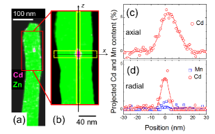
Figure 1c shows the SEM image of the NW, and Fig. 2a is an EDX image of the NW tip, showing the areas which are predominantly ZnTe and CdTe. Such images are qualitative. A quantitative analysis [8] is based on the intensity profiles across the QD, along the two perpendicular axes, Fig. 2c-d. A good fit of the radial intensity profile, Fig. 2d, was obtained [8] assuming a uniform composition, Cd0.9Mn0.1Te, in a cylinder of diameter 8 nm. The fit of the axial profile, Fig. 2c, is obtained using the expression proposed earlier[24]: a square profile of width , broadened by an exponential of characteristic size (reservoir effect) and a Gaussian of width , with nm, =3.5 nm and =5 nm. Other radial profiles have been measured and analyzed for several positions along the NW axis [8]: in addition to the Cd0.9Mn0.1Te QD, they clearly identify the (Zn,Mg)Te external shell, but also a very thin (Zn,Cd)Te internal shell due to lateral growth.
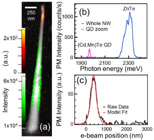
Figure 3 summarizes the CL results obtained on the same NW. Two features appear on the monochromatic images (a) and on the spectra (b): a broad structured band around 2300 meV, visible over the whole NW, and an instrumentally-broadened line at 1980 nm, detected only at the tip. The high-energy side of the green band coincides with the emission of ZnTe NWs with a (Zn,Mg)Te shell, i.e., the ZnTe exciton shifted by the strain induced by the (Zn,Mg)Te shell [23, 25, 26]. In addition, a low-energy tail is observed in Fig. 3b, that we ascribe to the presence of the shallow (Zn,Cd)Te internal shell. Such a tail, and structures at even lower energy, are observed in other NWs with CdTe insertions, and similar features have been identified as due to lateral QDs [27]. They can be efficiently eliminated by using adapted growth conditions [24].
The red emission is coming from a small region, located around the (Cd,Mn)Te insertion identified by EDX. The intensity is plotted in Fig. 3c as a function of the electron beam position. The active region is broader than the excitation volume (calculated to be 100 nm wide using the CASINO software[28]), showing that the electrons diffuse towards the QD over a typical diffusion length which we estimate to be 120 nm on both sides.
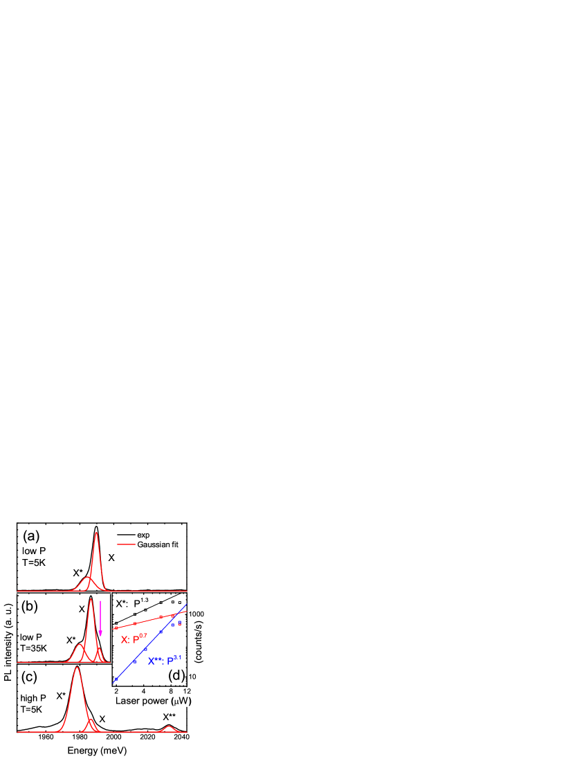
Complementary information on this red emission is obtained by micro-PL, Fig. 4, with a better spectral resolution. At low excitation density and low temperature, Fig. 4a, the spectrum is dominated by a line (labeled ) at 1989.6 meV, with a FWHM of about 5.5 meV; a weak satellite is observed on the low energy side at 1984.2 meV (labeled ), with a FWHM of 9 meV. This satellite strongly gains in intensity upon increasing the excitation density (Fig. 4c), and other lines appear (for instance, at 2040 meV). The three lines exhibit a markedly different power dependence, Fig. 4d. The slightly sublinear increase and saturation of line at 1989.6 meV suggests a neutral exciton state. The slightly superlinear increase of the satellite suggests a charged exciton or possibly a bi-exciton. The third line ( at 2040 meV) exhibits a strongly super-linear dependence which suggests a multi-excitonic state. Finally, at higher temperature, another line appears on the high-energy side (violet arrow in Fig. 4b) while the ratio between the two previous ones is not changed significantly: the new line will be attributed below to an excited state.
Photoluminescence spectra with a magnetic field applied perpendicular to the NW axis are shown in Fig. 5a: the line exhibits a strong red shift, up to 24 meV at 11 T and 6 K. The shift decreases as the temperature increases, as shown by the plot in Fig. 5b. This temperature-dependant redshift is a characteristic feature of the giant Zeeman effect in a diluted magnetic semiconductor such as (Cd, Mn)Te [29]: in the absence of anisotropy, the shift is expected to be proportional to the magnetization of the Mn spins, and hence to vary as a modified Brillouin function , where is the Landé factor of Mn, is the Bohr magneton and the Boltzmann constant, and is a characteristic temperature determined by the Mn content of the alloy [29, 30]. Fig. 5c shows that the redshift is indeed a saturating function of (provided we accept, as usual for PL spectra, a small heating of the Mn temperature, as indicated within parentheses). An example of the Brillouin function is shown by the blue dashed line: the agreement is good at high field, confirming that the saturation of the redshift reflects that of the Mn magnetization. There is however a clear deviation at low field, see Fig. 5d: we will show below that this deviation is due to the spin anisotropy of the holes, and that it agrees with a heavy-hole character.
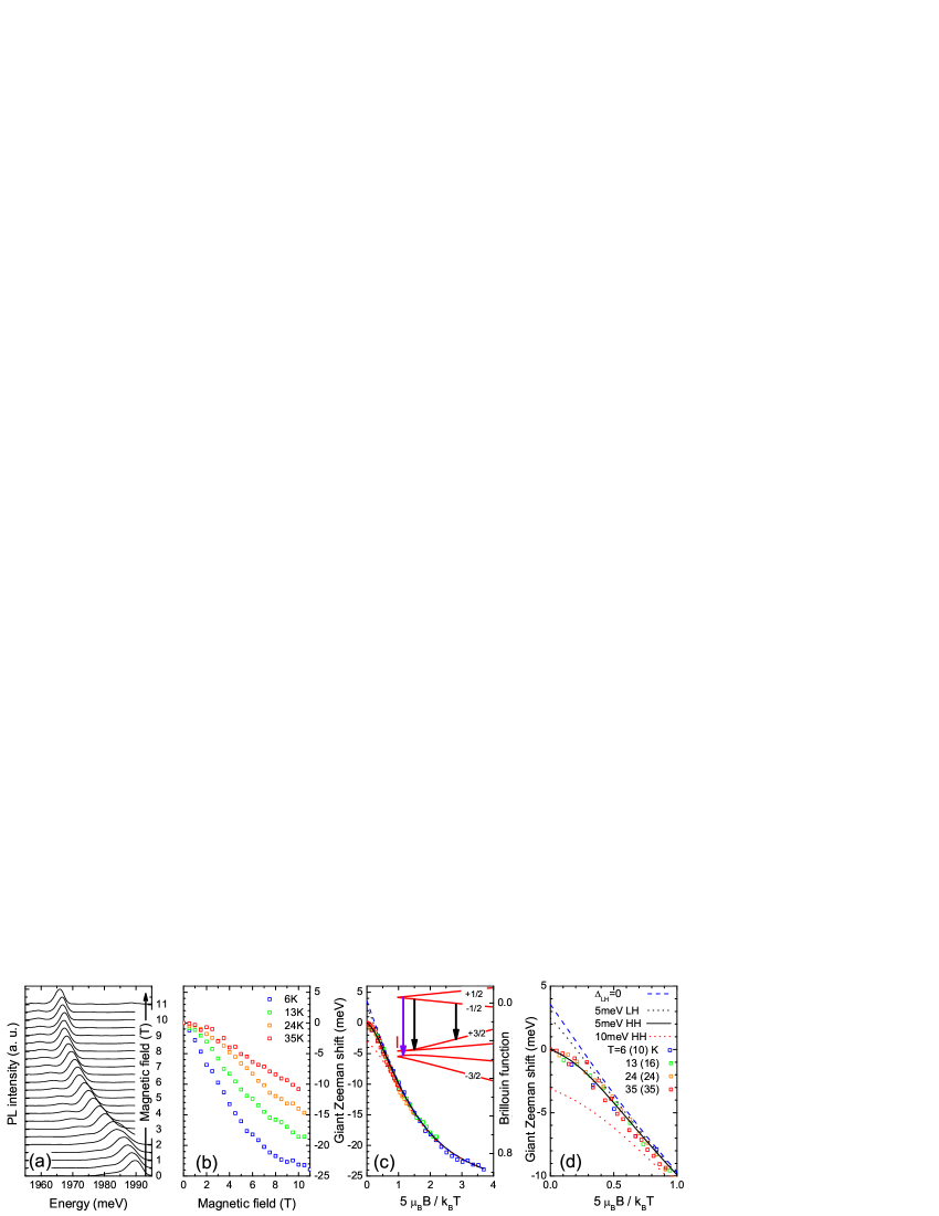
The energy of the photoluminescence line labeled X, and its dependence on the excitation density, appear to be quite similar to what is currently observed in self-assembled SK QDs made of the same materials [31]. In the present study, two correlated experiments support this assignment to the (Cd,Mn)Te QD: (1) the spatial localization of the CL emission coincides with the position of the QD as determined by EDX, (2) the presence of a large giant Zeeman effect which is expected from the presence of about 10% Mn in the QD as detected by EDX.
Note that the linewidth - much larger than in an usual, non-magnetic QD, including SK CdTe QD in ZnTe - is expected for a (Cd,Mn)Te QD and indeed experimentally observed in SK QDs [9] or QDs in NWs [10]. It however makes it impossible to check an antibunching effect (single photon emission) by a measure of correlations, such as for instance in CdSe QDs in ZnSe NWs [32] or CdTe QDs in ZnTe NWs [33].
4 Discussion
Coming back to the low-field behavior, we first use the simplest description of a (Cd,Mn)Te QD as initially developed for SK QD [9] and recently used for QDs in NWs [10]: it involves, in the valence band, a heavy-hole ground state and a light-hole excited state, with a splitting , and a giant Zeeman effect. Typical values of the splitting are meV in SK QDs [34] and =10 to 60 meV in QDs in NWs [10]. The giant Zeeman effect in bulk material is described by an exchange field parallel and proportional to the magnetization M of the Mn spins, with a Hamiltonian [29] where is the hole spin operator () and the magnetization is described by a Brillouin function , see above; is the Zeeman shift for Mn magnetization at saturation (, Brillouin function equal to unity). The electron state is described similarly by a giant Zeeman term . Experimentally, the maximum giant Zeeman shifts are observed for a uniform Mn content , and amount to meV for the electrons, and (if the magnetization is along the quantization axis) meV for the heavy hole and meV for the light hole [30]. The simplest adaptation to the case of QDs, the so-called exchange box model [35] gives similar expressions.
The solid line in Fig. 5c-d shows that a good fit of the shift of the ground-state neutral exciton and the excited state (observed at higher temperature), as a function of the applied field and for different values of the temperature, is obtained for the following values of the parameters: meV, meV, meV. A clear deviation is observed at low field if we fit the high-field data assuming a degenerate hole multiplet (): then the shift is simply proportional to the Brillouin function (upper, blue dashed line in Fig. 5c-d); a deviation is also observed if we assume a heavy-hole ground state with a larger splitting meV (lower, red dotted line), or a light-hole ground state (upper, black dotted line).
Let us discuss the values of the fitting parameters. The value of nicely matches the position of the excited line observed at high temperature (violet arrow in Fig. 4b at 35K, and in the inset of Fig. 5c). The values of the giant Zeeman splitting are smaller than expected for the Mn content measured by EDX: the reduction is small for the electron ( meV instead of 11 meV); it is larger for the heavy hole, meV instead of 44 meV, definitely beyond the error bar on . In addition, assuming a different value of the Mn content would affect both electrons and holes, hence it is ruled out. Such reduced values of the giant Zeeman splitting suggest that the electron envelope function, and even more that of the hole, are not strictly confined to the area of the Mn distribution. In this case, the Mn magnetization enters the expression of the giant Zeeman effect, with a weight given by the squared envelope function of the carrier: this causes a significant reduction if the carrier is not well confined in the QD. In the present case, the valence band offset between CdTe and ZnTe is small [36, 37], so that the holes are likely to be at least partly delocalized. Indeed, long lifetimes, in the ns range, have been measured in other QDs from the same sample, which also suggests a non total overlap of the electron and hole.
The most noticeable result is that the ground state is a heavy hole, with a very small splitting, 5 meV, from a light-hole excited state. This is smaller than the values of the splitting (10 to 60 meV) previously reported [10] for inclusions of unknown shape. A heavy-hole to light-hole crossing is expected when increasing the aspect ratio of a QD across a value close to unity for QDs with abrupt interfaces and strong valence band offset [1, 2], confirming the simple idea obtained for the ellipsoidal inclusion of an isotropic material in an infinite matrix with a smaller lattice parameter: the crossing is predicted at unity (sphere), both from the sign of the built-in axial shear strain (Eshelby model [16]) and from the confinement. Indeed, light-holes excitons have been confirmed in several other QDs from the same sample [3] as the present one. In the present QD, the crossing is not far but not reached yet, although the EDX profile unambiguously demonstrates an elongated shape.
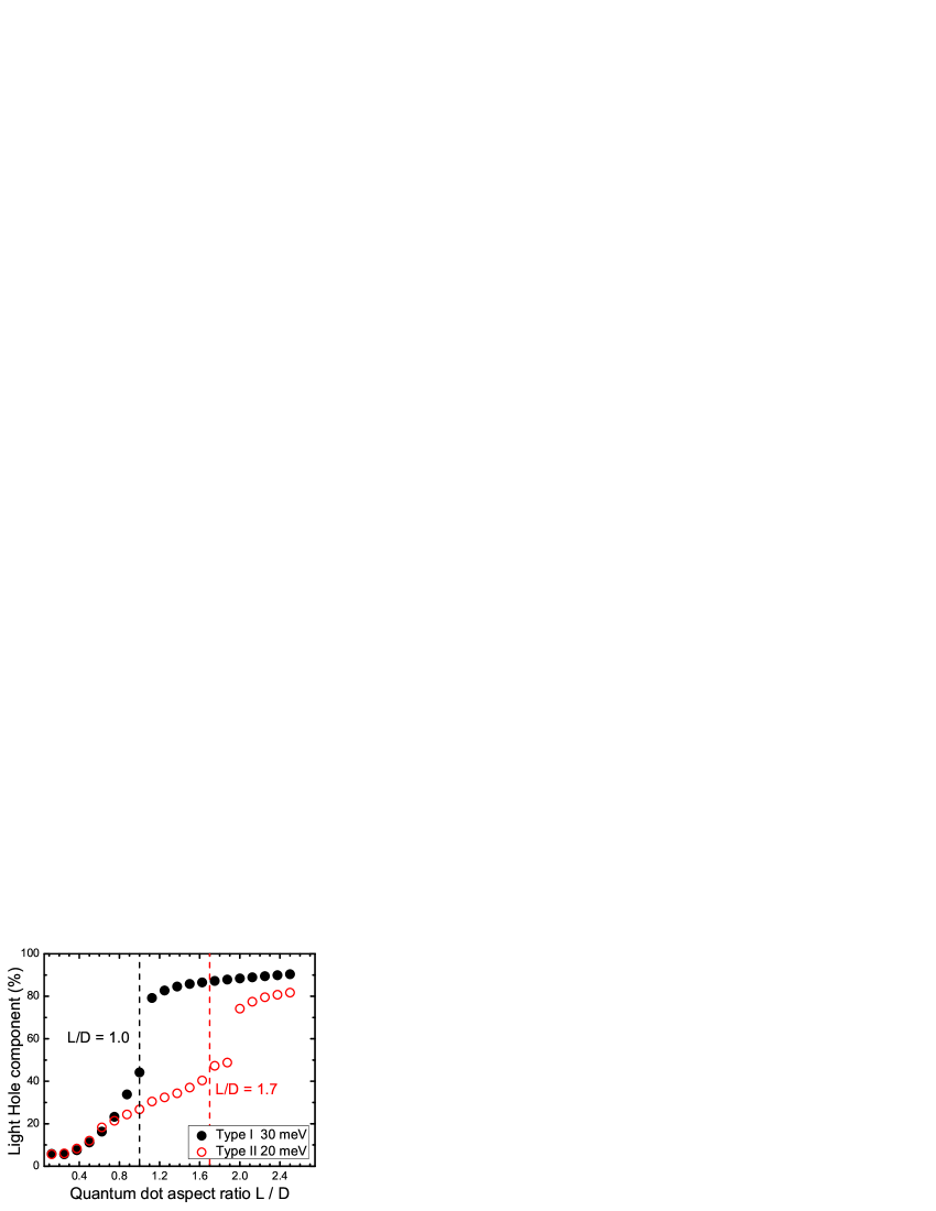
To understand the origin of a shift of the heavy-hole to light-hole crossing to values of the aspect ratio larger than one, we have performed a numerical calculation of the hole state in an ellipsoidal QD. The calculation takes into account the elastic coefficients, Bir-Pikus parameters, Luttinger parameters and piezoelectric coefficient of CdTe in the inclusion, and those of ZnTe in the ZnTe core and the Zn0.9Mg0.1Te outer shell. A critical parameter is the band offset between the inclusion material and the core material, which is known to be small for CdTe-ZnTe: photoelectron spectroscopy studies [36] conclude to a valence band offset between 50 meV (type I) and -100 meV (type II), while the optical spectroscopy of CdTe-(Cd,Zn)Te quantum wells [37] suggests a valence band offset equal to meV, strongly affected by the mismatch strain. Results of the calculation are displayed in Fig. 6 for a QD in a core-shell NW, for two values of the valence band offset within this range. This - and other results [38] not shown - show that the crossover from heavy-hole to light-hole remains close to , even for a small value of the valence band offset, provided the hole remains confined to the QD. If the valence band offset further decreases (red open circles in Fig. 6), the hole leaks into the core for values of around unity, and the mismatch with the external shell enhances the heavy-hole contribution, thus pushing the crossover to higher values of . As the introduction of 10% Mn in the CdTe inclusion increases the bandgap by meV, with about 1/3 in the valence band, the present sample is likely to correspond to this slightly type-II configuration, in agreement with the observation of a heavy-hole exciton with a long lifetime for an elongated inclusion. A CdTe inclusion possibly realizes the QD configuration represented by black solid circles in Fig. 6. To achieve the same configuration with a (Cd,Mn)Te QD, the inclusion must be fully embedded in a (Zn,Mg)Te NW with no ZnTe core [38]. A definitive conclusion calls for a systematic study with samples on both sides of the crossover, and the extension of the numerical calculation to address more complex QD morphologies and to incorporate excitonic effects.
5 Conclusion
To sum up, we have demonstrated that using a dedicated TEM grid / PL sample holder based on a silicon nitride membrane allows us to apply a broad range of experimental methods to the same, single nano-object. Here, scanning electron microscopy with low-temperature cathodoluminescence, transmission electron microscopy with energy-dispersive X-ray spectrometry, and low-temperature micro-photoluminescence with applied magnetic field, were applied to the same, single NW containing a QD.
EDX confirms the elongated shape of the inclusion, nm 12 nm, and its composition, Cd0.9Mn0.1Te. CL confirms the attribution of an emission line at eV to this inclusion, while another line at eV is due to the ZnTe shell. Magneto-optical spectroscopy identifies the heavy-hole character of the ground state exciton, with a sizable giant Zeeman effect. A quantitative study of the Zeeman effect suggests a significant delocalization of the heavy hole from the inclusion, and the presence of the light-hole exciton meV higher in energy, in agreement with the onset of a PL line when increasing the temperature from 6K to 35K. Finally, a numerical calculation underlines the role of the valence band offset and the effect of a mismatched shell in setting the quantum dot aspect ratio at which the crossover from heavy-hole to light-hole takes place: the valence band offset between CdTe and ZnTe, known to be small, is further reduced by the inclusion of Mn in CdTe, pushing the (Cd,Mn)Te in ZnTe QD towards a slightly type-II configuration; then the presence of a Zn0.9Mg0.1Te adds a strain tensile along the NW axis and gives a heavy-hole character to the hole ground state.
References
References
- [1] Niquet Y-M and Mojica D C 2008 Phys. Rev. B 77 115316
- [2] Zieliński M 2013 Phys. Rev. B 88 115424
- [3] Jeannin M, Artioli A, Rueda-Fonseca P, Bellet-Amalric E, Kheng K, André R, Tatarenko S, Cibert J, Ferrand D and Nogues G 2017 Phys. Rev. B 95 035305
- [4] Huo Y H, Witek B J, Kumar S, Cardenas J R, Zhang J X, Akopian N, Singh R, Zallo E, Grifone R, Kriegner D, Trotta R, Ding F, Stangl J, Zwiller V, Bester G, Rastelli A and Schmidt O G 2014 Nature Phys. 10 46
- [5] Haffouz S, Zeuner K D, Dalacu D, Poole P J, Lapointe J, Poitras D, Mnaymneh K, Xiaohua Wu, Couillard M, Korkusinski M, Schöll E, Jöns K D, Zwiller V and Williams R L 2018 emphNano Lett. 18 3047
- [6] Foster A P, Bradley J P, Gardner K, Krysa A B, Royall B, Skolnick M S and Wilson L R 2015 Nano Lett. 15 1559
- [7] Schlehahn A, Fischbach S, Schmidt R, Kaganskiy A, Strittmatter A, Rodt S, Heindel T and Reitzenstein S 2018 Scientific Reports 8 1340
- [8] Rueda-Fonseca P, Robin E, Bellet-Amalric E, Lopez-Haro M, den Hertog M, Genuist Y, André R, Artioli A, Tatarenko S, Ferrand D and Cibert J 2016 Nano Lett. 16 1637
- [9] Kłopotowski Ł, Cywinski L, Wojnar P, Voliotis V, Fronc K, Kazimierczuk T, Golnik A, Ravaro M, Grousson R, Karczewski G and Wojtowicz T 2011 Phys. Rev. B 83 081306(R)
- [10] Szymura M, Wojnar P, Kłopotowski Ł, Suffczyǹski J, Goryca M, Smoleǹski M, Kossacki P, Zaleszczyk W, Wojciechowski T, Karczewski G, Wojtowicz T and Kossut J Nano Lett. 15 1972
- [11] Płachta J, Grodzicka E, Kaleta A, Kret S, Baczewski L T, Pietruczik A, Wiater M, Goryca M, Kazimierczuk T, Kossacki P, Karczewski G, Wojtowicz T and Wojnar P 2018 Nanotechnology 29 205205
- [12] Delikanli S, Akgul M Z, Murphy J R, Barman B, Tsai Y, Scrace T, Zhang P, Bozok B, Hernández-Martínez P L, Christodoulides J, Cartwright A N, Petrou A and Demir H V 2015 ACS Nano 9 12473
- [13] Muckel F, Delikanli S, Hernández-Martínez P L, Priesner T, Lorenz S, Ackermann J, Sharma M, Demir H V and Bacher G 2018 Nano Lett. 18 2047
- [14] Guria A K, Dutta S K, Adhikari S D and Pradhan N 2017 ACS Energy Lett. 2 1014
- [15] Mir W J, Jagadeeswararao M, Das S and Nag A 2017 ACS Energy Lett. 2 537
- [16] Eshelby J D 1957 Proc. Royal Soc. A 241 376
- [17] http://inacceafr/LSim/TBSim
- [18] den Hertog M, Gonzalez-Posada F, Songmuang R, Rouvière J-L, Fournier T, Fernandez B and Monroy E 2012 Nano Lett. 12 5691-5696
- [19] Jiming Bao, Bell D C, Capasso, F Wagner J B , Mårtensson T, Trägårdh J and Samuelson L 2008 Nano Lett. 8 836
- [20] Senichev A, Corfdir P, Brandt O, Ramsteiner M, Breuer S, Schilling J, Geelhaar L and Werner P 2018 Nano Research 11 708
- [21] Auzelle T, Haas B, den Hertog M, Rouvière J-L, Daudin B and Gayral B, 2015 Appl. Phys. Lett. 107 051904
- [22] Rueda-Fonseca P, Orrù M, Bellet-Amalric E, Robin E, den Hertog M, Genuist Y, André R, Tatarenko S and Cibert J 2016 J. Appl. Phys. 119 164303
- [23] Artioli A, Rueda-Fonseca P, Stepanov P, Bellet-Amalric E, den Hertog M, Bougerol C, Genuist Y, Donatini F, André R, Nogues G, Kheng K, Tatarenko S, Ferrand D and Cibert J 2013 Appl. Phys. Lett. 103 222106
- [24] Orrú M, Robin E, den Hertog M, Moratis K, Genuist Y, André R, Ferrand D, Cibert J and Bellet-Amalric E 2018 Phys. Rev. Materials 2 043404
- [25] Wojnar P, Zielinski M, Janik E, Zaleszczyk W, Wojciechowski T, Wojnar R, Szymura M, Kopotowski L, Baczewski T, Pietruchik A, Wiater M, Kret S, Karczewski G, Wojtowicz T and Kossut J 2014 Appl. Phys. Lett. 104 163111
- [26] Ferrand D and Cibert J 2014 Eur. Phys. J. Appl. Phys. 67 30403
- [27] Wojnar P, Płachta J, Zaleszczyk W, Kret S, Sanchez Ana M, Rudniewski R, Raczkowska K, Szymura M, Karczewski G, Baczewski L T, Pietruczik A, Wojtowicz T and Kossut J 2016 Nanoscale 8 5720
- [28] http://wwwgelusherbrookeca/casino/Whathtml
- [29] Gaj JA, Planel R and Fishman G 1993 Solid State Communications 88 927
- [30] Gaj J A, Grieshaber W, Bodin C, Cibert J, Feuillet G, Merle d’Aubigné Y and Wasiela A 1994 Phys. Rev. B 50 5512
- [31] Clément T, Ferrand D, Besombes L, Boukari H, Mariette H 2010 Phys. Rev. B 81 155328
- [32] Bounouar S, Elouneg-Jamroz M, den Hertog M, Morchutt C, Bellet-Amalric E, André R, Bougerol C, Genuist Y, Poizat J-P, Tatarenko S and Kheng K 2012 Nano Lett. 12 2977-2981
- [33] Wojnar P, Janik E, Baczewski L T, Kret S, Karczewski G, Wojtowicz T, Goryca M, Kazimierczuk T and Kossacki P 2011 Appl. Phys. Lett. 99 113109
- [34] Léger J, Besombes L, Maingault L and Mariette H 2007 Phys. Rev. B 76 045331
- [35] Golnik A, Ginter J and Gaj J A 1983 J Phys C 16 6073
- [36] Späth B, Fritsche J and Klein A, Jaegermann W 2007 Appl. Phys. Lett. 90 062112
- [37] Calatayud J, Allègre J, Mathieu H, Magnea N and Mariette H 1993 Phys. Rev. B 47 9684
- [38] Moratis K, Orrù M, Bellet-Amalric E, Robin E, Nogues G, Donatini F, André R, Niquet Y-M, Cibert J and Ferrand D 2018 34th Internat. Conf. Phys. Semiconductors Montpellier