Single-Shot Readout Performance of Two Heterojunction-Bipolar-Transistor Amplification Circuits at Millikelvin Temperatures
Abstract
High-fidelity single-shot readout of spin qubits requires distinguishing states much faster than the T1 time of the spin state. One approach to improving readout fidelity and bandwidth (BW) is cryogenic amplification, where the signal from the qubit is amplified before noise sources are introduced and room-temperature amplifiers can operate at lower gain and higher BW. We compare the performance of two cryogenic amplification circuits: a current-biased heterojunction bipolar transistor circuit (CB-HBT), and an AC-coupled HBT circuit (AC-HBT). Both circuits are mounted on the mixing-chamber stage of a dilution refrigerator and are connected to silicon metal oxide semiconductor (Si-MOS) quantum dot devices on a printed circuit board (PCB). The power dissipated by the CB-HBT ranges from 0.1 to 1 W whereas the power of the AC-HBT ranges from 1 to 20 W. Referred to the input, the noise spectral density is low for both circuits, in the 15 to 30 fA/ range. The charge sensitivity for the CB-HBT and AC-HBT is 330 e/ and 400 e/, respectively. For the single-shot readout performed, less than 10 s is required for both circuits to achieve bit error rates below 10-3, which is a putative threshold for quantum error correction.
Introduction
Spin qubits in semiconductors are a promising platform for building quantum computers (Kane, 1998; Elzerman et al., 2004; Petta et al., 2005; Morello et al., 2010; Pla et al., 2013; Eng et al., 2015; Zajac et al., 2017; Rochette et al., 2017). Significant progress has been achieved in recent years, including demonstrations of extremely long coherence times (Muhonen et al., 2014), high-fidelity state readout (Harvey-Collard et al., 2018; Nakajima et al., 2017; Shulman et al., 2014; Watson et al., 2015), high-fidelity single qubits gates (Takeda et al., 2016; Muhonen et al., 2014; Kawakami et al., 2016; Nichol et al., 2017), and two qubit gates (Shulman et al., 2012; Nichol et al., 2017; Yoneda et al., 2018; Zajac et al., 2017). As the field advances to multiple qubit systems, improvements in single-shot state readout and measurement times will be necessary to achieve fault tolerance. Improving the signal-to-noise ratio (SNR) and bandwidth (BW) of the qubit state detection is critical for both tunnel rate selective readout (Elzerman et al., 2004) and energy selective readout (Petta et al., 2005). With the same bit error rate, faster readout will reduce tunnel rate and metastable relaxation or relaxation related errors.
Cryogenic amplification is one way the readout SNR and BW can be improved. Challenges are that: 1) input signals remain relatively small (Onac et al., 2006; Khrapai et al., 2006; Gustavsson et al., 2007; Horibe et al., 2015; Harvey-Collard et al., 2017) and 2) significant noise and parasitic capacitance is introduced into the measurement circuit when routing the signal out of a dilution refrigerator (Kalra et al., 2016). Several approaches for cryogenic amplification include: radio-frequency (RF) resonant quantum point contact (QPC) and single electron transistor (SET) circuits (Schoelkopf et al., 1998; Aassime et al., 2001; Reilly et al., 2007; Barthel et al., 2009, 2010; Mason et al., 2010; Yuan et al., 2012; Verduijn et al., 2014), gate dispersive RF circuits (Colless et al., 2013), Josephson parametric amplification circuits (Stehlik et al., 2015), and cryogenic transistors (Visscher et al., 1996; Pettersson et al., 1996; Vink et al., 2007; Curry et al., 2015; Tracy et al., 2016). For single-shot readout, qubit state distinguishability with sensitivity 140 e/ has been demonstrated (Barthel et al., 2010). However, many of these circuits require elements to be mounted at multiple fridge stages and the use of custom on-chip components, adding to the complexity of their implementation. Simpler amplification circuits that use low power transistors mounted directly on the mixing chamber stage with the qubit device thus have significant appeal (Tracy et al., 2016; Curry et al., 2015). For example, a proof of principle readout demonstration with a dual stage HEMT achieved Te = 240 mK, gain = 2700 A/A, power = 13 W, noise referred to input 70 fA/, and 350 e/ charge sensitivity (Tracy et al., 2016).
Silicon-germanium (SiGe) heterojunction bipolar transistors (HBTs) have been demonstrated to operate at liquid helium temperatures (Joseph et al., 1995; Curry et al., 2015) as well as millikelvin temperatures in dilution refrigerators (Najafizadeh et al., 2009; Curry et al., 2016; Ying et al., 2017; Davidović et al., 2017). The HBT is motivated by low 1/f noise, high Rout, and possible opportunities to achieve higher gain at the same power. Furthermore, there can be bipolar junction transistor (BJT) advantages compared to field effect transistors (FETs) for low input impedance amplifier circuits (Horowitz et al., 1980). Our approach is to use a single SiGe HBT as a cryogenic amplifier at the mixing chamber stage of a dilution refrigerator to improve the SNR and BW of the signal from a SET used as a charge-sensor. We have designed and characterized two different HBT circuits: 1) the current-biased HBT circuit (CB-HBT) (Figure 2(a)) and 2) the AC-coupled HBT circuit (AC-HBT) (Figure 1(a)). The CB-HBT simply has the drain of the SET connected to the base of the HBT, while the AC-HBT has the base of the HBT connected to the drain of the SET via a resistor-capacitor (RC) bias tee. Regardless of the coupling between the HBT and SET, the HBT must be DC biased in order to amplify. For either circuit, the silicon metal oxide semiconductor (Si-MOS) device and HBT are mounted on a printed circuit board (PCB) only centimeters apart. The proximity of the HBT amplifier to the SET has the advantages of minimizing parasitic input capacitance and increasing signal before noise from the fridge is added. However, since the mixing chamber stage has a cooling power of around 100 W at 100 mK, the HBT circuits must operate with powers similar or less in order to avoid heating.
In this letter, we first introduce the two amplification circuits with discussions of gain, sensitivity, bias behavior, and noise. We compare the basic performance and operation of the two amplifiers and extract input-referred noise as well as signal response and heating of the quantum dot electrons. Finally, we compare and discuss the performance for single-shot readout, which somewhat depends on the specific layout of the SET and quantum dot to produce larger signals via increased mutual capacitance.
AC-HBT Description
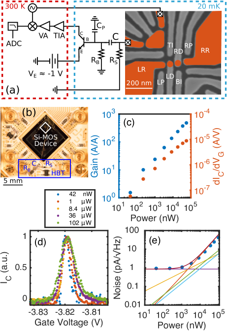
The AC-HBT consists of a Si-MOS device that is AC-coupled to an HBT, which amplifies the SET response to AC source-drain voltage excitation at frequencies higher than around 100 Hz. The SET is integrated into a double quantum dot (QD) device (Figure 1(a): SEM image), which is made on a Si-MOS platform (see Appendix A).
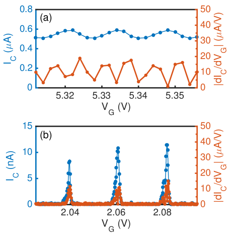
To operate the AC-HBT, the DC base bias is grounded, and the emitter is biased negatively to support a base-emitter bias above the cryogenic HBT threshold (about -1.04 V). The HBT current at the collector is measured through a room temperature transimpedance amplifier (TIA), and the signal is demodulated, filtered, and digitized. The TIA is referenced to ground, so the collector-emitter bias equals the base-emitter bias. We find that this configuration optimizes the circuit SNR and also requires only two lines coming from room temperature for the three HBT terminals. Figure 1(c) shows the total AC circuit gain and sensitivity vs. the amount of power dissipated by the HBT. The AC gain is measured by comparing the current of a Coulomb blockade (CB) peak with and without the HBT. The SET current can be measured directly by connecting the output of to a room temperature TIA (lowest ground in Figure 1(a)). The sensitivity of the circuit is defined as the gate-voltage derivative of collector-current (slope) on the side of a CB peak, which is the typical bias point where readout occurs. Sensitivities of 1-5 A/V are achieved in the operating region of the AC-HBT. Since the AC-HBT is a linear amplifier, the shape of a CB peak remains unaffected by different gain/sensitivity bias points of the AC-HBT (Figure 1(d)). The AC bias across the SET was chosen to be 200 VRMS in this case to minimize the electron temperature below 200 mK.
Noise spectra are collected for different AC-HBT biases (see Appendix F), and noise at around 74 kHz is referred to the HBT collector and studied. The noise displays two different behaviors as power dissipated is increased (Figure 1(e)). The transconductance of the transistor () increases with power, so it is important to identify where the transistor begins to add appreciable noise. In the low-power limit, the noise dependence is approximately flat at around 1 pA/, which we attribute to the noise after the HBT dominating any AC-HBT noise. As the AC-HBT power is increased to > 1 W, the noise becomes linearly dependent on power. This behavior is predicted by our estimated shot noise for the base current (Figure 1(e) orange curve). The estimated total noise is calculated by adding all noise source predictions in quadrature (dark red curve) and aligns well with the total measured noise (blue points).
CB-HBT Description
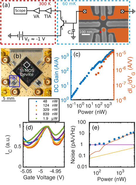
The CB-HBT circuit consists of an HBT wire bonded from its base terminal directly to the drain of the SET. The SET is integrated into a double QD system consisting of a lithographic QD and a secondary object that has not been definitively identified (i.e., either a QD (Jock et al., 2018) or donor (Harvey-Collard et al., 2017)). A high-frequency coaxial line is connected to the collector of the HBT which is used to measure the readout current (Figure 2(a)). This collector line is connected to a TIA which is set with gain 105 V/A and -3 dB bandwidth 400 kHz unless otherwise noted. The output of the TIA is connected to a voltage amplifier used to limit the bandwidth or further amplify the signal. Finally, the output of the voltage amplifier is connected to an oscilloscope with an adjustable sample rate.
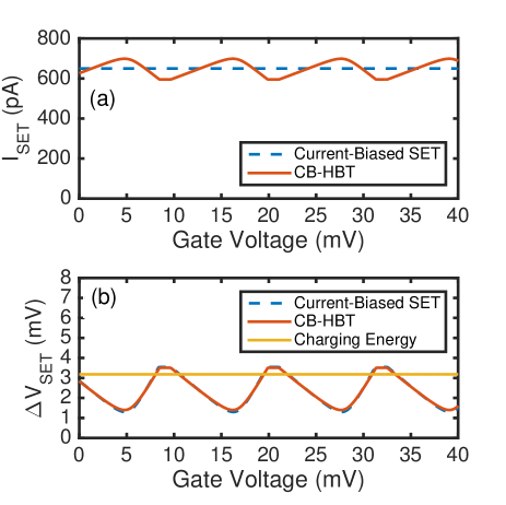
Operation of the circuit requires the emitter of the HBT to be connected to a room temperature power supply filtered to 1 MHz (to suppress higher frequency noise) and biased between -1.03 and -1.07 V. The bias of the emitter power supply sets the base current, collector current, gain, and dissipated power of the HBT. In Figure 2(b), the DC current gain and sensitivity are plotted as a function of power. The DC current gain is defined as , and the sensitivity is defined as before. The sensitivity of the CB-HBT can reach 5 A/V between 100-500 nW, whereas the AC-HBT requires > 10 W to reach a similar sensitivity.
The CB-HBT acts as a current bias, so there is always current through the SET (see Appendix B). In regions of Coulomb blockade, the HBT base-emitter voltage will shift on the order of the charging energy of the SET in order to maintain a relatively constant current through the circuit. To show the current-biasing effect, a CB peak is plotted for different CB-HBT gain values in Figure 2(d), and the current is normalized to the value at the top of the CB peak. Although the current in the blockaded regions of the CB peak is much different from a voltage-biased configuration, the slope of the sides of the CB peak appear to be less affected by the current-biasing (sensitivities of 1–5 A/V are achieved for either circuit). We note that the effect of current bias on Coulomb blockade is independent of the HBT presence (Figure 7).
As with the AC-HBT, the noise referred to the collector of the CB-HBT is examined at around 7 kHz (Figure 2(d)). Similar qualitatively, the lower power region is dominated by noise after the HBT around 1 pA/ (purple curve). As power is increased, the measured noise (blue points) begins to increase, which follows the estimated behavior of the base current shot-noise (orange curve) (see Appendix F).
Amplifier Performance Comparison
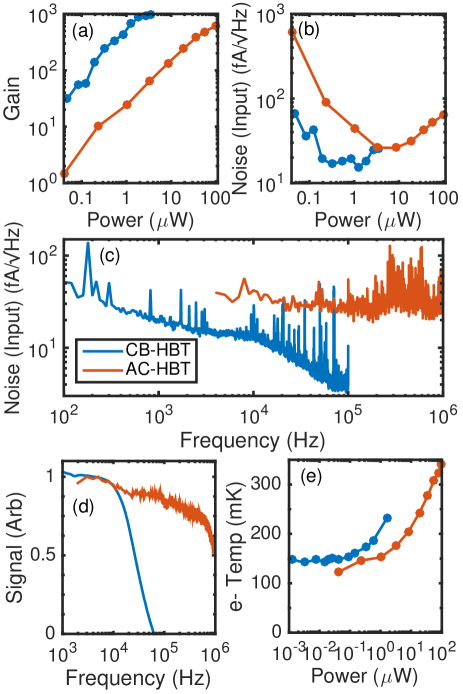
We next compare the performance of both amplifiers with respect to power dissipated. The first metric examined is gain as power is increased. The gain of the AC-HBT is simply the measured gain of the amplifier, however the gain of the CB-HBT circuit is not as simple to extract. The small-signal resistance of the SET (rset) must be known in order to calculate the CB-HBT gain (see Appendix E). Since the SET is directly connected to the HBT, we cannot measure rset. Instead, we use the value of rset (3 MΩ) which best follows the measured noise behavior in Figure 2(e) to estimate the gain. We plot this estimated gain of the CB-HBT circuit and compare to the measured gain of the AC-HBT circuit in Figure 3(a). We observe that the CB-HBT circuit achieves higher gain at lower powers, including operating with gain over 400 at a power around 1 W.
We next compare the noise referred to the input of the HBT for each circuit. Noise is referred to the input using the gain values in Figure 3(a). We measure the noise spectrum for each circuit at different bias points and choose the frequency which minimizes the noise. The frequency chosen for the AC-HBT circuit was around 74 kHz, and the frequency for the CB-HBT circuit was around 7 kHz. When the input-referred noise is plotted as a function of power (Figure 3(b)), we observe a minimum noise operating point for either circuit. At low powers, the noise is likely dominated by triboelectric noise due to the fridge and input noise of the room temperature TIA. At higher powers, the HBT amplifiers begin injecting appreciable noise into the circuit, therefore the overall noise increases. The CB-HBT circuit achieves a minimum noise of 19 fA/ at a power around 800 nW, while the AC-HBT circuit achieves a minimum noise of 26 fA/ at a power around 8.4 W.
For the powers that minimize noise for each circuit, we plot the input-referred noise spectrum for both circuits as a function of frequency (Figure 3(c)). The noise spectrum of the CB-HBT is plotted out to 100 kHz, since its bandwidth is less than 100 kHz. The 1/f-like behavior of the noise at lower frequencies is assumed to be due to charge noise in the Si-MOS device. In the overlapping region around 10 kHz, the noise for the CB-HBT is significantly lower than the noise for the AC-HBT.
Figure 3(d) shows the frequency dependence of an input signal for both amplification circuits up to 1 MHz. The AC-HBT has a -3 dB point at around 650 kHz, and the CB-HBT has a -3 dB point at around 20 kHz, which implies significantly lower BW than the AC-HBT. The origin of this lower BW is not well understood. Using pessimistic numbers, the frequency pole of the SET resistance (assuming 1 MΩ) and the parasitic capacitance between the SET and the base junction (assuming 1 pF) should only limit the -3 dB point to around 160 kHz. In addition, 4 K simulations of this circuit also yielded around 160 kHz -3 dB BW (England et al., 2017). Improvements and understanding of the BW of the CB-HBT will be important in future work.
Heating of electrons in the QD due to the operation of the connected HBT is a concern, therefore we examined the dependence of electron temperature on HBT amplifier bias (Figure 3(e)). For the CB-HBT, we find that the minimum electron temperature observed is around 150 mK. Heating of the QD begins where the CB-HBT is operating with over 100 gain at 100 nW, therefore the CB-HBT circuit can amplify well with an electron temperature around 160–200 mK. For the AC-HBT, the minimum electron temperature was around 120 mK. When the AC-HBT bias is increased up to 3.24 W, the electron temperature remains near the minimum temperature. For powers above this threshold, the electron temperature increases approximately linearly with power. Nonetheless, an electron temperature of 200 mK is used for the bias condition that provides the minimum amplifier noise.
Single-Shot Results Comparison
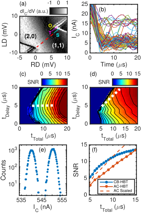
We compare both HBT amplifiers by performing single-shot readout of latched charge states (Harvey-Collard et al., 2018). Both Si-MOS quantum dot devices are tuned to the few electron regime and the spin filling of the last few transition lines are verified with magnetospectroscopy. Figure 4(a) shows the result of a three-level pulse sequence in the AC-HBT device where: 1) the system is initialized into (1,0), 2) ground and excited states are loaded in (2,0), and finally 3) the measurement point (signal plotted) is rastered about the (2,0)-(1,1) anti-crossing. When measuring for 30 s, three latched lines are present, which indicates spin blockade for an excited state triplet (T), a second excited state triplet (O), and a lifting of the spin blockade for the ground state singlet (S). We assign T as a valley triplet with valley splitting of 140 eV and the O as an orbital triplet with orbital splitting of 280 eV. For all single-shot measurements, we remove the state O from the available state space by energy selective loading of the (2,0) state.
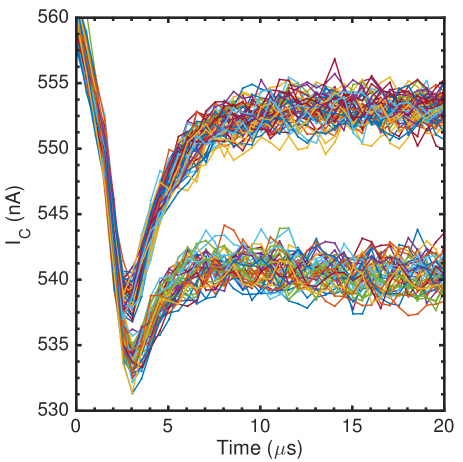
For both circuits, a mixture of (2,1) and (2,0) charge states are read out in the reverse latching window. Figure 4(b) shows 100 individual single-shot traces of the readout portion of the pulse for the AC-HBT device. Significant feedthrough is observed in the first few s of the readout pulse, likely due to attenuators connecting the conductor of the high BW lines to the ground of other lines including the emitter bias line. State distinguishability does not begin to occur until about 4 s, and then the pulse relaxes to two distinct states after about 7 s. Extracting the SNR from these traces is done by waiting a certain amount of time, tdelay, and then averaging the signal for a certain amount of time, tintegration. Histograms of the delayed and averaged shots are compiled and fit to a double Gaussian distribution (Figure 4(c)). The signal is defined as the separation of the Gaussian peaks and the noise is defined as the average of the widths of the Gaussian peaks.
The extracted SNR for a given delay and total time (tdelay + tintegration) is plotted in Figures 4(d)&(e). Contours are drawn for each SNR integer on both plots, where the leftmost part of a contour line reveals the minimum total measurement time required to reach a given SNR. We plot the SNR vs. minimum total measurement time in Figure 4(f) for both circuits. The CB-HBT reaches greater SNR at any given time in the 15 s plot range. Both circuits achieve SNR > 7 in ttotal < 10 s, which corresponds to a bit error rate < 10-3 and marks a significant improvement over the equivalent ttotal = 65 s in previous work (Harvey-Collard et al., 2018). In particular, the CB-HBT is able to reach SNR > 7 in ttotal 6 s, which represents over a factor of ten improvement from the previous work (Harvey-Collard et al., 2018). The charge sensitivity for the CB-HBT is 330 e/ (τint = 6 s, SNR = 7.4), and the charge sensitivity for the AC-HBT is 400 e/ (τint = 9 s, SNR = 7.5). We note that the SET in the CB-HBT device had around 34% more signal due to larger mutual capacitance (Appendix A) which may contribute to the larger SNRs.
The AC-HBT requires more relative overhead for implementation than the CB-HBT. The AC-HBT includes three additional surface mounted passive elements (Figure 1(a)), which can be optimized to produce better SNR. Additionally, the AC-HBT has a two-dimensional bias space via the base bias and emitter bias, whereas the CB-HBT is only biased via the emitter bias. However, the AC-HBT is a linear gain circuit and can be used with discrete HEMTs (Tracy et al., 2018) and HBTs, providing more opportunity to optimize the transistor. Ideally, the transistors would have greater transconductance (gm) and a more ideal dependence on IC than the HBTs used in this work (see Appendix D). In the present demonstration of the AC-HBT, heating of electrons occurred at powers which minimized noise. Introducing a second AC-HBT stage is relatively straightforward and may allow the first stage to run at powers which don’t heat the electrons and minimize the noise further. In addition, the second stage could be mounted further away from the Si-MOS PCB and reduce local heating.
Conclusion
We compare the performance of two cryogenic amplification circuits: the CB-HBT and the AC-HBT. The power dissipated by the CB-HBT ranges from 0.1 to 1 W, whereas the power of the AC-HBT ranges from 1 to 20 W. Referred to the input, the noise spectral density is low for both circuits in the 15 to 30 fA/ range. The charge sensitivity for the CB-HBT and AC-HBT is 330 e/ and 400 e/, respectively. For single-shot readout performed, both circuits achieve SNR > 7 and bit error rate < 10-3 in times less than 10 s.
Acknowledgements.
This work was performed, in part, at the Center for Integrated Nanotechnologies, an Office of Science User Facility operated for the U.S. Department of Energy (DOE) Office of Science. Sandia National Laboratories is a multi-mission laboratory managed and operated by National Technology and Engineering Solutions of Sandia, LLC, a wholly owned subsidiary of Honeywell International, Inc., for the DOE’s National Nuclear Security Administration under contract DE-NA0003525. This paper describes objective technical results and analysis. Any subjective views or opinions that might be expressed in the paper do not necessarily represent the views of the U.S. Department of Energy or the United States Government.References
- Kane (1998) B. E. Kane, Nature 393, 133 EP (1998).
- Elzerman et al. (2004) J. M. Elzerman, R. Hanson, L. H. Willems van Beveren, B. Witkamp, L. M. K. Vandersypen, and L. P. Kouwenhoven, Nature 430, 431 EP (2004).
- Petta et al. (2005) J. R. Petta, A. C. Johnson, J. M. Taylor, E. A. Laird, A. Yacoby, M. D. Lukin, C. M. Marcus, M. P. Hanson, and A. C. Gossard, Science 309, 2180 (2005).
- Morello et al. (2010) A. Morello, J. J. Pla, F. A. Zwanenburg, K. W. Chan, K. Y. Tan, H. Huebl, M. Möttönen, C. D. Nugroho, C. Yang, J. A. van Donkelaar, A. D. C. Alves, D. N. Jamieson, C. C. Escott, L. C. L. Hollenberg, R. G. Clark, and A. S. Dzurak, Nature 467, 687 EP (2010).
- Pla et al. (2013) J. J. Pla, K. Y. Tan, J. P. Dehollain, W. H. Lim, J. J. L. Morton, F. A. Zwanenburg, D. N. Jamieson, A. S. Dzurak, and A. Morello, Nature 496, 334 EP (2013).
- Eng et al. (2015) K. Eng, T. D. Ladd, A. Smith, M. G. Borselli, A. A. Kiselev, B. H. Fong, K. S. Holabird, T. M. Hazard, B. Huang, P. W. Deelman, and et al., Science Advances 1, e1500214 (2015).
- Zajac et al. (2017) D. M. Zajac, A. J. Sigillito, M. Russ, F. Borjans, J. M. Taylor, G. Burkard, and J. R. Petta, Science , eaao5965 (2017).
- Rochette et al. (2017) S. Rochette, M. Rudolph, A.-M. Roy, M. Curry, G. T. Eyck, R. Manginell, J. Wendt, T. Pluym, S. Carr, D. Ward, et al., arXiv preprint arXiv:1707.03895 (2017).
- Muhonen et al. (2014) J. T. Muhonen, J. P. Dehollain, A. Laucht, F. E. Hudson, R. Kalra, T. Sekiguchi, K. M. Itoh, D. N. Jamieson, J. C. McCallum, A. S. Dzurak, and A. Morello, Nature Nanotechnology 9, 986 EP (2014).
- Harvey-Collard et al. (2018) P. Harvey-Collard, B. D’Anjou, M. Rudolph, N. T. Jacobson, J. Dominguez, G. A. Ten Eyck, J. R. Wendt, T. Pluym, M. P. Lilly, W. A. Coish, M. Pioro-Ladrière, and M. S. Carroll, Phys. Rev. X 8, 021046 (2018).
- Nakajima et al. (2017) T. Nakajima, M. R. Delbecq, T. Otsuka, P. Stano, S. Amaha, J. Yoneda, A. Noiri, K. Kawasaki, K. Takeda, G. Allison, A. Ludwig, A. D. Wieck, D. Loss, and S. Tarucha, Phys. Rev. Lett. 119, 017701 (2017).
- Shulman et al. (2014) M. D. Shulman, S. P. Harvey, J. M. Nichol, S. D. Bartlett, A. C. Doherty, V. Umansky, and A. Yacoby, Nature Communications 5, 5156 EP (2014).
- Watson et al. (2015) T. F. Watson, B. Weber, M. G. House, H. Büch, and M. Y. Simmons, Phys. Rev. Lett. 115, 166806 (2015).
- Takeda et al. (2016) K. Takeda, J. Kamioka, T. Otsuka, J. Yoneda, T. Nakajima, M. R. Delbecq, S. Amaha, G. Allison, T. Kodera, S. Oda, and S. Tarucha, Science Advances 2 (2016), 10.1126/sciadv.1600694.
- Kawakami et al. (2016) E. Kawakami, T. Jullien, P. Scarlino, D. R. Ward, D. E. Savage, M. G. Lagally, V. V. Dobrovitski, M. Friesen, S. N. Coppersmith, M. A. Eriksson, and L. M. K. Vandersypen, Proceedings of the National Academy of Sciences 113, 11738 (2016).
- Nichol et al. (2017) J. M. Nichol, L. A. Orona, S. P. Harvey, S. Fallahi, G. C. Gardner, M. J. Manfra, and A. Yacoby, npj Quantum Information 3, 3 (2017).
- Shulman et al. (2012) M. D. Shulman, O. E. Dial, S. P. Harvey, H. Bluhm, V. Umansky, and A. Yacoby, Science 336, 202 (2012).
- Yoneda et al. (2018) J. Yoneda, K. Takeda, T. Otsuka, T. Nakajima, M. R. Delbecq, G. Allison, T. Honda, T. Kodera, S. Oda, Y. Hoshi, N. Usami, K. M. Itoh, and S. Tarucha, Nature Nanotechnology 13, 102 (2018).
- Onac et al. (2006) E. Onac, F. Balestro, L. H. W. van Beveren, U. Hartmann, Y. V. Nazarov, and L. P. Kouwenhoven, Phys. Rev. Lett. 96, 176601 (2006).
- Khrapai et al. (2006) V. S. Khrapai, S. Ludwig, J. P. Kotthaus, H. P. Tranitz, and W. Wegscheider, Phys. Rev. Lett. 97, 176803 (2006).
- Gustavsson et al. (2007) S. Gustavsson, M. Studer, R. Leturcq, T. Ihn, K. Ensslin, D. C. Driscoll, and A. C. Gossard, Phys. Rev. Lett. 99, 206804 (2007).
- Horibe et al. (2015) K. Horibe, T. Kodera, and S. Oda, Applied Physics Letters 106, 053119 (2015).
- Harvey-Collard et al. (2017) P. Harvey-Collard, N. T. Jacobson, M. Rudolph, J. Dominguez, G. A. Ten Eyck, J. R. Wendt, T. Pluym, J. K. Gamble, M. P. Lilly, M. Pioro-Ladrière, and M. S. Carroll, Nature Communications 8, 1029 (2017).
- Kalra et al. (2016) R. Kalra, A. Laucht, J. P. Dehollain, D. Bar, S. Freer, S. Simmons, J. T. Muhonen, and A. Morello, Review of Scientific Instruments 87, 073905 (2016).
- Schoelkopf et al. (1998) R. J. Schoelkopf, P. Wahlgren, A. A. Kozhevnikov, P. Delsing, and D. E. Prober, Science 280, 1238 (1998).
- Aassime et al. (2001) A. Aassime, G. Johansson, G. Wendin, R. J. Schoelkopf, and P. Delsing, Phys. Rev. Lett. 86, 3376 (2001).
- Reilly et al. (2007) D. J. Reilly, C. M. Marcus, M. P. Hanson, and A. C. Gossard, Applied Physics Letters 91, 162101 (2007).
- Barthel et al. (2009) C. Barthel, D. J. Reilly, C. M. Marcus, M. P. Hanson, and A. C. Gossard, Phys. Rev. Lett. 103, 160503 (2009).
- Barthel et al. (2010) C. Barthel, M. Kjærgaard, J. Medford, M. Stopa, C. M. Marcus, M. P. Hanson, and A. C. Gossard, Physical Review B 81 (2010).
- Mason et al. (2010) J. Mason, S. A. Studenikin, B. Djurkovic, A. Sachrajda, J. Kycia, L. Gaudreau, S. Studenikin, and A. Patricia Kam, Physica E: Low-dimensional Systems and Nanostructures 42 (2010).
- Yuan et al. (2012) M. Yuan, Z. Yang, D. E. Savage, M. G. Lagally, M. A. Eriksson, and A. J. Rimberg, Applied Physics Letters 101, 142103 (2012).
- Verduijn et al. (2014) J. Verduijn, M. Vinet, and S. Rogge, Applied Physics Letters 104, 102107 (2014).
- Colless et al. (2013) J. I. Colless, A. C. Mahoney, J. M. Hornibrook, A. C. Doherty, H. Lu, A. C. Gossard, and D. J. Reilly, Physical Review Letters 110 (2013).
- Stehlik et al. (2015) J. Stehlik, Y.-Y. Liu, C. M. Quintana, C. Eichler, T. R. Hartke, and J. R. Petta, Phys. Rev. Applied 4, 014018 (2015).
- Visscher et al. (1996) E. H. Visscher, J. Lindeman, S. M. Verbrugh, P. Hadley, J. E. Mooij, and W. van der Vleuten, Applied Physics Letters 68, 2014 (1996).
- Pettersson et al. (1996) J. Pettersson, P. Wahlgren, P. Delsing, D. B. Haviland, T. Claeson, N. Rorsman, and H. Zirath, Phys. Rev. B 53, R13272 (1996).
- Vink et al. (2007) I. T. Vink, T. Nooitgedagt, R. N. Schouten, L. M. K. Vandersypen, and W. Wegscheider, Applied Physics Letters 91, 123512 (2007).
- Curry et al. (2015) M. J. Curry, T. D. England, N. C. Bishop, G. Ten-Eyck, J. R. Wendt, T. Pluym, M. P. Lilly, S. M. Carr, and M. S. Carroll, Applied Physics Letters 106, 203505 (2015).
- Tracy et al. (2016) L. A. Tracy, D. R. Luhman, S. M. Carr, N. C. Bishop, G. A. Ten Eyck, T. Pluym, J. R. Wendt, M. P. Lilly, and M. S. Carroll, Applied Physics Letters 108, 063101 (2016).
- Joseph et al. (1995) A. J. Joseph, J. D. Cressler, and D. M. Richey, IEEE Electron Device Letters 16, 268 (1995).
- Najafizadeh et al. (2009) L. Najafizadeh, J. S. Adams, S. D. Phillips, K. A. Moen, J. D. Cressler, S. Aslam, T. R. Stevenson, and R. M. Meloy, IEEE Electron Device Letters 30, 508 (2009).
- Curry et al. (2016) M. Curry, T. England, J. Wendt, T. Pluym, M. Lilly, S. Carr, and M. Carroll, Bulletin of the American Physical Society 61 (2016).
- Ying et al. (2017) H. Ying, B. R. Wier, J. Dark, N. E. Lourenco, L. Ge, A. P. Omprakash, M. Mourigal, D. Davidovic, and J. D. Cressler, IEEE Electron Device Letters 38, 12 (2017).
- Davidović et al. (2017) D. Davidović, H. Ying, J. Dark, B. R. Wier, L. Ge, N. E. Lourenco, A. P. Omprakash, M. Mourigal, and J. D. Cressler, Phys. Rev. Applied 8, 024015 (2017).
- Horowitz et al. (1980) P. Horowitz, W. Hill, and I. Robinson, The Art of Electronics, Vol. 2 (Cambridge University Press Cambridge, 1980).
- Jock et al. (2018) R. M. Jock, N. T. Jacobson, P. Harvey-Collard, A. M. Mounce, V. Srinivasa, D. R. Ward, J. Anderson, R. Manginell, J. R. Wendt, M. Rudolph, T. Pluym, J. K. Gamble, A. D. Baczewski, W. M. Witzel, and M. S. Carroll, Nature Communications 9, 1768 (2018).
- England et al. (2017) T. England, M. Curry, S. Carr, A. Mounce, R. Jock, P. Sharma, C. Bureau-Oxton, M. Rudolph, T. Hardin, and M. Carroll, Bulletin of the American Physical Society 62 (2017).
- Tracy et al. (2018) L. Tracy, J. Reno, and T. Hargett, Bulletin of the American Physical Society (2018).
- Nordberg et al. (2009) E. P. Nordberg, H. L. Stalford, R. Young, G. A. Ten Eyck, K. Eng, L. A. Tracy, K. D. Childs, J. R. Wendt, R. K. Grubbs, J. Stevens, M. P. Lilly, M. A. Eriksson, and M. S. Carroll, Applied Physics Letters 95, 202102 (2009).
- Knapp et al. (2018) T. Knapp, J. Dodson, B. Thorgrimsson, D. Savage, M. Lagally, S. Coppersmith, and M. Eriksson, Bulletin of the American Physical Society 63 (2018).
- Beenakker and Schönenberger (2003) C. Beenakker and C. Schönenberger, Physics Today 56, 37 (2003).
- Kafanov and Delsing (2009) S. Kafanov and P. Delsing, Phys. Rev. B 80, 155320 (2009).
Appendix A SET Geometries And Details
The SET connected to the AC-HBT uses a single layer doped poly-Si electrode structure on 50 nm thick SiO2, providing a mobility of 19,500 cm2/Vs at 4 K. The poly-Si gate layer is etch-defined into electrodes that control the formation of the SET (upper left in Figure 1(a) SEM image) and two quantum dots (under gates RD and LD). Regions of electron enhancement are indicated by the highlighted regions.
The Si-MOS device in the CB-HBT circuit is similar to the Si-MOS device in the AC-HBT circuit with the exception that the SiO2 layer is 35 nm thick and the bottom layer is isotopically purified silicon (500 ppm 29Si). The 28Si isotope has no net nuclear spin, therefore it is ideal for qubits to be formed in because decoherence due to magnetic noise is highly suppressed. Phosphorous (31P) donor atoms are imbedded in the 28Si layer using ion implantation near where the quantum dot is intended to be formed (red dot in Figure 2(a) SEM image).
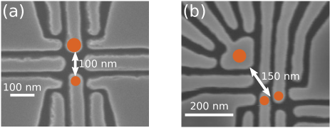
The CB-HBT and AC-HBT were characterized using different Si-MOS devices possessing different electrostatic gate layouts (Figure 5). The geometry of the gate layout affects the mutual capacitance between the SET and the quantum dot. More capacitive coupling results in larger changes in the electrochemical potential of the charge-sensor for a given quantum dot charging event (Nordberg et al., 2009). Since changes in electrochemical potential of the charge-sensor result in changes in current through the charge-sensor, larger changes result in larger signal. Therefore, more mutual capacitance leads to larger readout signals, faster readout times, and higher readout fidelity.
The gate geometry used in the Si-MOS device connected to the CB-HBT had the SET 33% closer to the quantum dot than in the Si-MOS device connected to the AC-HBT. The closer SET proximity in the CB-HBT resulted in an increase in sensitivity of approximately 34%. We compare the sensitivity of both circuits by dividing the voltage shift of the dot occupancy transition by the charge-sensor Coulomb blockade peak period. For the CB-HBT, the voltage shift was 18 mV and the charge-sensor period was 337 mV (5.34% change). For the AC-HBT, the voltage shift was 12 mV and the charge-sensor period was 350 mV (4% change). Therefore, the SET in the CB-HBT was around 34% more sensitive to charging events than the AC-HBT.
Appendix B Current-Biasing Effect of CB-HBT Circuit
Since the node that connects the SET source to the HBT base is floating, the bias across the SET cannot be set to a fixed voltage in the CB-HBT circuit. Verilog-A models were created to simulate the behavior of the circuit when biasing the SET through multiple regions of Coulomb blockade via an electrostatic gate. As the SET resistance changes due to Coulomb blockade, the source-drain bias across the SET changes to allow current to flow into the base of the HBT (Figure 7(b)). In order for this to happen, the HBT trades base-emitter voltage for minimal impact to operation. Although the trade in voltage results in a relatively small change in HBT collector current during, for example, a single-shot readout event, this signal is approximately 100 larger than the SET source-drain signal without an HBT (e.g. ΔIC = 10 nA vs. ΔISET = 100 pA).
The Verilog-A model estimates the small signal resistances as: rset = 200 kΩ and rπ = 10 MΩ (where rπ is the small signal resistance of the base-emitter junction). Most of the emitter bias voltage is across the base-emitter junction at all times (since rset << rπ), therefore the CB-HBT is a current-biasing circuit. The current-biasing behavior is highlighted in Figure 8(a), where three Coulomb blockade peaks are plotted. For comparison, three Coulomb blockade peaks are plotted for the AC-HBT case (Figure 8(b)). The CB-HBT amplified peaks are broadened by the current-biasing effect and the blockade region never reaches zero current as it would with a smaller constant voltage bias. The AC-HBT amplified peaks are much narrower and minimally broaden due to having a constant, small voltage bias regardless of HBT power. Comparable sensitivities can be achieved for either circuit around 10 A/V.
Appendix C Electron Temperature Measurement
Heating of electrons in the quantum dot due to the operation of the connected HBT is a concern, therefore we examined the dependence of electron temperature on HBT amplifier bias (Figure 3(e)). For the CB-HBT, The electron temperature of the QD was measured by extracting the width of a Coulomb blockade peak as a function of fridge temperature. The QD was tuned to a transport regime where the QD was approximately equally tunnel-coupled to both reservoirs and there were around 10 electrons in the QD. The source-drain bias was reduced to 5 Vrms to avoid bias heating. A Coulomb peak was chosen where a minimum width was observed in Coulomb diamond measurements. After extracting the lever-arm of the gate used to measure the broadening (13 eV/mV), we find that the minimum linewidth yields an electron temperature around 150 mK. Heating of the QD begins where the CB-HBT is operating with over 100 gain, therefore the CB-HBT circuit can amplify well while heating the electrons to 160–200 mK.
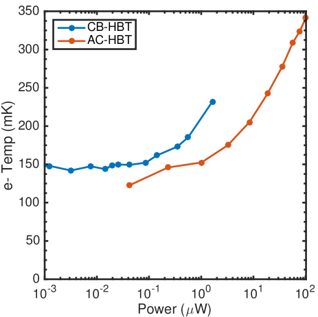
For the AC-HBT setup, the base electron temperature was around 120 mK. This is confirmed by the measurements of the electron temperature when measuring the SET signal directly through the shunt resistor (RS in Figure 1(a)) with the HBT turned off. With the HBT on, The electron temperature is deduced by measuring the Fermi-Dirac linewidth of the (1,0)-(2,0) charge transition. When the AC-HBT bias is increased up to 3.24 W, the electron temperature remains near the base temperature (Figure 9). For powers above this threshold, the electron temperature increases approximately linearly with power. This might be due to local heating of the PCB and wires, which increase the temperature of the nearby device (Knapp et al., 2018). No effort has been made to heat sink the AC-HBT in this experiment, so further tests with various heat sinking options will be performed to minimize the increase in electron temperature. Nonetheless, an electron temperature of 200 mK is achieved for the bias condition that provides the minimum amplifier noise.
Appendix D HBT Characterization
Before being used in either amplification circuit, HBTs are initially characterized in liquid helium at 4 K using PCBs with eight HBTs mounted on them. We find that HBT performance at 4 K—particularly current gain vs. base current—changes minimally when HBTs are cooled down to 20–60 mK in a dilution refrigerator (Figure 10(b)). This is most likely due to the charge-carrier transport mechanism changing from a drift-diffusion regime (temperature dependent) to a tunneling regime (barrier dependent) at around 30 K (Davidović et al., 2017).
In order to characterize HBTs, Keithley 2400 source-measure units are used as current meters and connected to the HBT base and collector terminals. A power supply (emitter bias) is connected to the HBT emitter terminal and used to bias the HBT to different operating regimes. The emitter bias has to reach approximately -1 V for the HBT to begin operating in an amplifying regime. As the emitter bias is changed from -1.00 V to around -1.07 V, the collector and base current begin to increase exponentially. The current gain, defined by dividing the collector current by the base current, also increases exponentially as emitter bias changes.
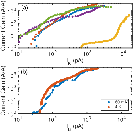
Previous measurements without HBT amplification circuits indicate that the SET current should be below several hundred pA in order to avoid QD electron heating. For the CB-HBT, we select HBTs based on their current gain at low base currents. Around 20% of HBTs characterized will have current gain > 100 at base current < 200 pA (Figure 10(a)). For the AC-HBT, the transconductance (gm) is the only metric required for selection. Since the HBTs were fabricated with gm as a primary metric, > 80% of HBTs are usable for the AC-HBT circuit even at low temperatures. However, gm does not scale ideally in these HBTs at cryogenic temperatures. For a given HBT, , where in normal conditions. In the HBTs used in this work, , which leads to suboptimal SNR at higher power.
Appendix E CB-HBT Small Signal Gain
The gain of the CB-HBT is calculated using a standard BJT small-signal model. A small voltage fluctuation at the base node is usually converted to a large current fluctuation at the collector node by the transconductance, gm = . This voltage fluctuation is usually the small-signal base-emitter junction resistance, rπ, multiplied by the base current. However, in the case of the CB-HBT, , therefore the parallel combination of the two resistances is required to calculate gain:
| (1) |
Appendix F Noise Models
Sources of noise in the HBT amplification circuits include: shot noise, Johnson noise, triboelectric noise associated with the coaxial lines coupled to fridge vibration (Kalra et al., 2016), room temperature amplifier noise, and other instrumental noise. At relatively low power operation regimes (< 1 W for the AC-HBT and < 200 nW for the CB-HBT), the noise due to vibrations in the fridge dominates at around 1 pA/. The input noise spectral density of the room temperature amplifier is relatively low (100–500 fA/), therefore we focus on noise sources much more dominant. When either circuit is operating in a regime appropriate for single-shot readout, the base shot noise is greater than the collector shot noise (Figures 1(e) and 2(e)). For the SET shot noise in either case, we do not consider a Fano factor, which would reduce the noise for a given power (Beenakker and Schönenberger, 2003; Kafanov and Delsing, 2009). The total noise for either circuit is calculated by assuming noise sources are independent processes and adding noise sources in quadrature.
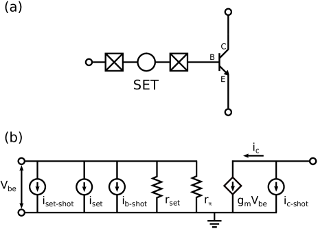
Noise modeling for the CB-HBT circuit is nontrivial because of current division at the HBT base node since . The SET and base current are reduced to a Norton equivalent circuit, and the HBT is reduced to rπ connected to a current source which takes voltage fluctuations (vbe) across rπ and converts them to collector current via the transconductance, gm. For the CB-HBT, the noise model is a shot noise current source (, where is the DC base current, and is the bandwidth centered on frequency ) in parallel with rset and rπ (Figure 12(b)). Since , most of the shot noise current goes through the SET to ground, and a much smaller amount enters the HBT base and is amplified. The amplified base shot noise is shown in Equation 2:
| (2) |
This amplified base shot noise is estimated in Figure 2(e) as the orange curve where gm and rπ are calculated from Gummel plots of the HBT and rset is assumed to be 3 MΩ, which was verified in later measurements with the HBT disconnected from the Si-MOS device.

The noise model for the AC-HBT is similar to the CB-HBT with rS and rB added in parallel to rset and rπ. The coupling capacitor, C, is considered a short at the frequencies appropriate to model noise in the AC-HBT. The Johnson noise of RS in the AC-HBT circuit is (where is the temperature) and does not contribute significantly in the single-shot operation regime. Since the AC-HBT has a separate current to bias the base-emitter junction, , therefore the base shot noise and SET shot noise are considered separately. However, , so the base shot noise is always dominant in amplifying regimes.
Appendix G AC-HBT Bias Tee Parameters
The bias tee parameters for the AC-HBT were chosen to be RS = 100 kΩ and C = 10 nF, which sets a high pass filter at 160 Hz. Operating the circuit at frequencies higher than 160 Hz aids in avoiding higher noise levels at lower frequency due to 1/f-like noise behavior in the system.
The shunt resistance value is chosen to be less than rset (100s of kΩ) so that most of the SET bias voltage drops across the SET.