Coulomb excitations and decays in graphene-related systems
Abstract
The layered graphene systems exhibit the rich and unique excitation spectra arising from the electron-electron Coulomb interactions. The generalized tight-binding model is developed to cover the planar/buckled/cylindrical structures, specific lattice symmetries, different layer numbers, distinct configurations, one-three dimensions, complicated intralayer and interlayer hopping integrals, electric field, magnetic quantization; any temperatures and dopings simultaneously. Furthermore, we modify the random-phase approximation to agree with the layer-dependent Coulomb potentials with the Dyson equation, so that these two methods can match with other under various external fields. The electron-hole excitations and plasmon modes are greatly diversified by the above-mentioned critical factors; that is, there exist the diverse (momentum. frequency)-related phase diagrams. They provide very effective deexcitation scatterings and thus dominate the Coulomb decay rates. Graphene, silicene and germanene might quite differ from one another in Coulomb excitations and decays because of the strength of spin-orbital coupling. Part of theoretical predictions have confirmed the experimental measurements, and most of them require the further examinations. Comparisons with the other models are also made in detail.
Corresponding author.
Tel: +886-7-717-2930.
E-mail addresses:
giorgio@mail.nknu.edu.tw (C. W. Chiu),
Corresponding author.
Tel: +886-6-275-7575.
E-mail addresses:
mflin@mail.ncku.edu.tw (M. F. Lin)
1 Introduction
The graphene-related systems have attracted a lot of theoretical and experimental researches, mainly owing to the unique hexagonal symmetry, unusual layered structures/nanoscaled thickness, and various stacking configurations.[9, 8, 7, 6, 3, 1, 2, 15, 4, 16, 5, 17] Such systems are very suitable for exploring the basic science and the high-potential applications.[9, 8, 7, 6, 5, 4, 3, 1, 2, 10, 11, 12, 13, 14] Electronic excitations/deexcitations arising from the electron-electron Coulomb interactions are one of essential physical properties, being closely related to the geometric and band structures. They are determined by the intrinsic many-particle properties and play a critical role in all the condensed-matter systems with the different dimensions. A new theoretical framework is developed for the layered systems; a modified random-phase approximation (RPA) is conducted on the 2D materials. In this book, a systematic and thorough investigation clearly indicate the diverse Coulomb excitation/decay phenomena, in which it covers many -bonding carbon-created materials, e.g., monolayer graphene, double-layer graphene, AA-, AB- ABC- AAB-stacked graphenes, sliding bilayer graphene, simple graphite, Bernal graphite, rhombohedral graphite, metallic/semiconducting carbon nanotubes, and monolayer silicene/germanene. The composite effects due to lattice symmetry, layer number, dimensionality, stacking configuration, temperature, doping, electric field, magnetic field will be discussed in detail. Specially, the magneto-electronic excitations, which are associated with the magnetic quantization, require the combination of the generalized tight-binding mode and the modified RPA. The theoretical predictions are fully compared with the experimental measurements from the electron energy loss spectroscopy (EELS), and part of them are consistent with the latter. The measured EELS spectra have confirmed the diverse collective excitations (plasmon modes) of the free carriers, and the valence electrons at different frequency ranges (the detailed discussions in Chap. 2.5).
The dielectric function () and the dimensionless energy loss (Im) function, which, respectively, represent the bare and screened response ability of charged carriers under the Coulomb field perturbation, are critical in fully understanding the intrinsic excitation/decay properties/of condensed-matter materials. In general, the imaginary part of and the prominent peaks in Im, respectively, correspond to the single-particle and collective excitations (electron-hole excitations and plasmon modes). is strictly defined for bulk graphites,[18] monolayer graphene,[18] and cylindrical carbon nanotubes,[19] since such systems possess a good translational symmetry, respectively, in the 3D, 2D and 1D spaces. That is to say, the bare Coulomb electron-electron interactions mainly determined by the transferred momentum () exhibit well-behaved/dimension-determined forms. On the other hand, the longitudinal dielectric function is expressed as a tensor form for the layered graphenes. The layer-projection method, which is closely related to the Coulomb scattering of the initial and final electronic states, will be introduced to deal with the electric polarizations. As a result, is a layer-dependent tensor function with the double indices (; the layer index), in which the band-structures effects on the excitation spectra and Coulomb matrix elements are fully taken into account in the theoretical model. For example, a -layer graphene possesses pairs of valence and conduction bands due to the carbon orbitals, and the sublattice-decomposed wave functions are utilized to accurately evaluate the layer-dependent or . Under the Born approximation, the effective energy loss function is characterized by the inelastic scattering probability of the incident electron beam. It has been very successfully in understanding the diverse electronic excitation spectra in layered systems, e.g., AA-,[21, 22, 23, 24] AB-[24, 28, 27] and ABC-stacked graphenes.[29] The magnetoplasmon is discussed in this book by the development of the modified RPA and the generalized Peierls tight-binding model.[30, 31, 32, 33] It is very suitable for studying the inter-landau-level (inter-LL), single-particle excitations and magneto-plasmon modes.[34, 35, 36] Moreover, electronic excitation spectra are also quite efficient decay channels by the inelastic Coulomb scatterings, being the strong effects on the energy widths of the quasiparticle states (the excited electrons or holes). The Coulomb decay rates are evaluated from the self-energy method under the detailed derivations. They will show certain important differences among monolayer graphene, silicene and germanene with the electron/hole doping. As to the experimental side, EELS and inelastic X-ray scatterings (IXS) are two very powerful techniques in providing Coulomb excitation phenomena. Their recent developments [37, 38] and measurements on the screened response functions of graphene-related materials[39, 40, 41, 42] are explored in detail. Also, the quasi-particle energy spectra under the measurements of the angle-resolved photo-emission spectroscopy (ARPES) are useful in the determinging the Coulomb decay rates.[43, 44, 45]
Monolayer graphene, as displayed in Fig. 1-1(a), has a planar honeycomb lattice composed of two equivalent sublattices, so that it exhibits the linear and isotropic Dirac-cone bans structure near the Fermi level ().[2] A pristine system is only a zero-gap semiconductor, since density of states (DOS) is vanishing at . The low-lying DOS is a linear V-shape form centered at .[2] It leads to the specific interband e-h excitations and the absence of intraband ones.[2] Temperature could induce the thermal excitations between the gapless valence and conduction states; that is, it generates conduction electrons and valence holes. The free carrier density per area is identified to reveal a simple -dependence, and their magnitude is estimated to e/cm2 at room temperature. The intraband single-particle excitations are induced/enhanced by temperature, while the great reduce is observed in the interband ones. Most important, temperature can create intraband plasmon modes at sufficiently high T, in which they belong to 2D acoustic collective excitations defined by a specific -dependence at long wavelength limit. By means of the alkali-adatom absorptions or the applications of gate voltages,[46, 47, 48, 49] there exists a very high free-carrier density ( e/cm2) in an extrinsic graphene system. The intraband interband excitations and the intraband plasmons are expected to be very pronounced in the bare and screened excitation spectra, respectively. This has been clearly confirmed from the EELS measurements.[42] Monolayer band structure is also reliable when the interlayer distance is very large (e.g., more than double that of graphite).[50] The effects, which purely arise from the interlayer Coulomb interactions, could be investigated for a double-layer graphene system. The acoustic and optical plasmon modes are clearly revealed in the EELS spectra, and they, respectively, correspond to the collective oscillations of two-layer charge carriers in phase and out of phase.[51, 52] The experimental measurements are required to verify these two modes.
The layered graphenes present the various stacking configurations, such as, AAA, ABA, ABC and AAB ones. The symmetries of geometric structures have strong effects on band structures and thus greatly diversify Coulomb excitations/decays. The AA stacking means that carbon atoms in different layers possess the same projections, as shown in Fig. 1-1(b). From the first-principles evaluations using VASP,[53] the ground state energy of the AA-stacked graphene is predicted to be highest among all the stacking configurations. This clearly indicates that it is relatively difficult to synthesize the AA stacking in the experimental laboratory.[54] According to both VASP and tight-binding model calculations,[32, 55] there exist pairs of Dirac-cone structures in the N-layer AA stacking; furthermore, such linear energy bands are intersecting at the K/K′ valley even in the presence of the vertical and non-vertical interlayer hopping integrals. For example, two pairs of valence Dirac cones in bilayer system are identified from the measurements of angle-resolved photoemission spectroscopy (ARPES) on the quasi-particle energy spectrum.[56, 57] The valence and conduction bands strongly overlap one another so that a lot of free electrons and holes are created by the interlayer atomic interactions. This semi-metallic property is in sharp contrast with the semiconducting behavior of monolayer graphene. Such carriers further induce the collective excitations in which the number of plasmon modes is identical to that of layer.[21] Also, the single-particle excitation channels are complicated/enriched by more energy bands. From the theoretical point of view, the interlayer hopping integrals and the interlayer Coulomb interactions need to be simultaneously included in the analytic formulas; that is, the band-structure effects are thoroughly covered in the electronic excitations/deexcitations. The main features of plasmon modes and electron-hole (e-h) dampings, the sensitive dependences on the transferred momentum and energy [()], are worthy of a systematic investigation. In addition, the experimental measurements are absent up to now.
The AB-stacked graphenes frequently appear in the experimental observations using the various methods, e.g., the successful syntheses by the mechanical exfoliation,[1, 58] the chemical vapor deposition (CVD),[60, 59] and the electrostatic manipulation of scanning tunneling microscopy (STM).[61, 62] This shows that their ground state energies are much lower than those of the AA stackings.[58] The AB stacking is the natural periodical sequence of Bernal graphite.[63, 64] The neighboring layers are attracted together by the weak but significant van der Waals interactions, so that the few-layer AB stacking could be obtained from the natural graphite under the mechanical action.[1, 58] They only possess half of carbon atoms in the same projections (Fig. 1-1(c)), or they are characterized by a relative shift of the C-C bond length () along the armchair direction about the initial AA stacking. There are more complex interlayer hopping integrals and extra site energies due to the different chemical environments experienced by the Al and Bl sublattices ( layer index), compared with the AA stacking. For AB bilayer stacking, the Dirac-cone energy bands become two pairs of parabolic valence and conduction bands, in which the latter are also initiated from the K/K′ valley (the corners of the hexagonal first Brillouin zone). Furthermore, the trilayer system presents an extra Dirac cone with a slight distortion. Such band-structure characteristics of few-layer AB stackings have been confirmed by the ARPES measurements[66, 65, 67, 68]. In short, a even- (an odd-) AB stacking exhibits pairs of parabolic bands (accompanied with a weakly separated Dirac-cone structure). In general, a small overlap of valence and conduction bands is revealed in the first pair of few-layer systems.[66] Apparently, the 2D free electron/hole density purely arising from the interlayer interactions is very low, leading to the absence of collective excitations in pristine AB-stacked systems.[69, 70] However, extrinsic few-layer AB stackings are expected to present the unusual Coulomb excitation behaviors (Chap. 5).
The ABC stacking, corresponding to Fig. 1-1(d)), is predicted to have the lower ground state energy than that of the ABA stacking.[55] The ABC-stacked few-layer graphenes are easily synthesized in the experimental growth.[58, 59, 60] However, its 3D counterpart, rhombohedral graphite, is only presented with a low-concentration arrangement in natural graphite; that is, most of 3D graphite belongs to the ABA (Bernal) stacking.[63, 64] The unique geometric symmetry induces the rich hopping integrals and the unusual electronic structures. The hopping integrals, which arise from the neighboring and next-neighboring layers, cover the vertical and non-vertical interlayer atomic interactions. The band structures exhibit three pairs of partially flat, sombrero-shaped and linear energy bands; the distinct energy dispersions centered at the K point have been verified from the ARPES experiments.[68, 67, 66] Specifically, the first pair just overlaps/touches at , leading to a sharp density of states (DOS). Such electronic wave functions are ascribed to the special surface states due to the main contributions of carbon atoms in the outmost two layers.[2, 71, 32] Although the ABC stacking is a semimetal with a very low free carrier density, it is predicted to exhibit the low-frequency plasmom mode closely related to the localized states.[29] Furthermore, the novel momentum dependence of the pristine plasmons is never observed in other stackings. On the other hand, the doping carriers in extrinsic systems will strongly compete with the original surface states. It is expected to create dramatic changes in the characteristics of e-h dampings and plasmon modes during the variation of .
The AAB stacking is the direct combination of AA and AB stackings, as displayed in Fig. 1-1(e). Such system has been successfully synthesized and experimentally observed by the distinct methods, e.g., the mechanical exfoliation directly by a scalper or scotch tape,[72] the CVD growth on SiC substrate[73] and Ru(0001) surface,[74] the liquid-phase exfoliation of natural graphite in N-methyl-2-pyrrolidone[75], and the STM.[77, 78, 79, 80, 62, 81, 82] In particular, the AAB stacking could be obtained by the rotating or horizontal shifting of the top graphite layer along the armchair direction. That is to say, the stacking configuration is continuously changed under the electrostatic modulation of STM. Furthermore, the corresponding DOS is also measured, indicating a narrow energy gap in trilayer ABA stacking.[74, 83] According to the first-principles method, the ground state energies per unit cell of six carbon atoms in trilayer graphenes are evaluated for the our stacking configurations. They are estimated as follows: 55.832866 eV, 55.857749 eV, 55.862386 eV and 55.864039 eV for AAA, AAB, ABA and ABC stackings, respectively.[55] The theoretical calculations predict that the AAB stacking is more stable than the AAA one, or the former presents the more promising future in experimental syntheses. The lower-symmetry AAB stacking possess the most complicated interlayer hopping integrals, in which this special property is clearly identified from a consistent/detailed comparison between the tight-binding model and VASP calculations in the low-lying energy bands.[84, 85] For example, the AAB-stacked trilayer graphene exhibits three pairs of energy bands with the oscillatory, sombrero-shaped and parabolic dispersions, in which the first ones determine a very band gap of meV. Of course, the semiconducting pristine system only creates the inter--band e-h excitations, but not the low-frequency plamsons. The doping effects on the Coulomb excitations are the first theoretical study, and the greatly diversified phenomena are described in Chap. 7.
How to create the dramatic transitions of essential properties is one of the main-stream topics in pristine graphenes. The continuous stacking configurations, which possess the high and low geometric symmetries, could enrich and diversify the physical phenomena. The sliding bilayer graphene presents the transformation between the highly symmetric stackings, being an ideal system for fully exploring the electronic topological transitions. There are some experimental successful syntheses, such as, the stacking boundaries including the relative shifts between neighboring graphene layers by the CVD method,[76] the sliding of graphene flakes on graphene substrate/micrometer-size graphite flakes initiated by the STM tip[77, 78], and AFM tip[79] and the electrostatic-manipulation STM performed on a highly oriented pyrolytic graphite (HOPG) surface.[82, 80, 62, 81] Specifically, the last method has generated a continuous and large-scaled movement of the top graphene layer, so that the sliding bilayer graphene is expected to be achieved by this method. The theoretical model calculations are focused on the electronic,[91, 92, 86, 87, 88, 89, 90] magnetic,[93] optical,[94, 95] transport[97, 98, 96] and phonon [99, 100, 101, 102] properties. For example, two low-lying isotropic Dirac cones are dramatically transformed into two pairs of parabolic bands during the variation of AAAB.[93, 87] Furthermore, the sliding bilayer graphene exhibits three kinds of Landau levels (LLs), the well-behaved, perturbed and undefined LLs, and three magneto-optical selection rules of , 1 2 (: the quantum number for each LL).[93, 30] During the continuous variation of stacking configuration, energy bands present the serious distortions and free carrier density show the drastic changes.[93, 30] These are predicted to induce the novel Coulomb excitation phenomena in pristine and extrinsic systems.
The external electric and magnetic fields are one of the critical factors in the creation of the diverse electronic excitations. A uniform perpendicular electric field () could be achieved by applying a gate voltage on a layered graphene system. There are a lot of such experimental setups up to now, being verified to have strong effects on transport properties and thus potential applications in nano-electronic devices.[103, 104, 105, 106] creates the distinct Coulomb potential energies on the layer-dependent sublattices. Apparently, energy dispersions and band gap are drastically changed by , in which the semi-metal-semiconductor transitions might occur as varies[107, 108]. The effects of on band structures are also diversified by the stacking configurations; that is, the -enriched energy bands are sensitive to the AAA, ABA, ABC and AAB stackings (the detailed discussions on Chap. 9). From the current model calculations of the modified RPA, a pristine -layer AAA stacking has one acoustic plasmon mode and optical ones,[22, 23] in which the former and the latter, respectively, originate from the intraband and the interband electronic excitations. An electric field obviously results in the charge transfer among the different graphene layers; therefore, it could modulate the number, frequency and intensity of collective excitation modes, e.g., the emergence of new plasmon modes and the decline of threshold plasmon frequency. As for the AB bilayer stacking, the low-frequency plasmon, which corresponds to the intraband single-particle excitations, is generated by a sufficiently high .[28] This greatly contrasts with a pristine system with any plasmon mode.[24] Such result directly illustrate that the -induced oscillatory parabolic bands, with the high DOSs, could create new plasmon modes, or the main features of band structures could determine the single-particle and collective excitations. The similar effects are revealed in the trilayer ABA and ABC stackings.[69, 29] This work will cover the complete results in the -enriched excitation spectra of the ABA, ABC and AAB stackings.
A uniform magnetic field () could flock together the neighboring electronic states and thus generate the highly-degenerate LLs and the special wave functions in the oscillatory forms. Apparently, the magnetic quantization is directly reflected in magneto-electronic excitations, belonging to a new topic of the Coulomb interactions, The LL characteristics, which are thoroughly explored by the generalized tight-binding model,[30, 31, 32, 33] cover the normal or abnormal spatial probability distributions with the regular/irregular zero-point numbers, the definition of quantum number from the domination sublattice, the dependences of energy spectrum on and , the non-crossing/crossing/anti-crossing behaviors, and the specific magneto-optical selection rules.[30, 33] They strongly depend on the number of layer and stacking configuration, i.e., they are greatly diversified by the geometric factors. The charged particles under experience a transverse magnetic force. The cyclotron motions present rather strong competitions with the longitudinal plasma oscillations due to the electron-electron interactions. This critical mechanism is responsible for the unusual excitation phenomena. Up to date, there are only few theoretical predictions on the magneto-plasmon modes of monolayer and AA/AB bilayer graphenes.[34, 35, 36] The direct combination of the generalized tight-binding model and the modified RPA is a developed theoretical framework. In addition to temperature, a magnetic field in monolayer graphene could drive a lot of discrete magneto-plasmons even under the low-energy range, mainly owing to the inter-LL excitations. Their oscillation frequencies exhibit the critical transferred momenta and the non-monotonous momentum dependence. Moreover, the quantized magneto-plasmons and the 2D acoustic plasmon mode might coexist in the AA bilayer stacking, but not the AB one. This difference lies in the stacking-dependent free carrier densities.
Graphite is one of the most extensively investigated materials experimentally and theoretically, being much more than 100 years. This layered system is very suitable/ideal for studying the diverse 3D and 2D physical phenomena; furthermore, it possesses a lot of up-to-date applications. Graphite crystals consist of a series of stacked graphene plane. Generally, there exist three kinds of stacking configurations in the layered graphites and compounds, namely AA, AB and ABC stackings. Simple hexagonal, Bernal and rhombohedral graphites exhibit the unusual essential properties as a result of the honeycomb lattice and stacking sequence. Among them, the AB-stacked graphite is predicted to to be the most stable system, according to the first-principles calculations on the ground state energy.[53] Natural graphite is composed of the dominating AB stacking and the partial ABC one.[63, 64] The AA-stacked graphite, which possesses the highest-symmetry crystal structure, does not survive in nature. The periodical AA stacking is frequently observed in the Li-intercalation graphite compounds.[109] Simple hexagonal graphite has been successfully synthesized by using the dc plasma in hydrogen-methane mixtures.[110] For the AA-. AB- and ABC-stacked graphites, the first/third system owns the highest/lowest 3D free carrier density.[33] Their low-energy band structures, respectively, present the -plane Dirac cones, the monolayer/bilayer characteristics at the H/K point, and the spiral Dirac-cone structure.[33] The ARPES measurements on Bernal graphite have verified the linear and parabolic energy dispersions near the H and K valleys.[111, 112, 113, 114] The theoretical studies of Coulomb excitations are focused on the free-carrier-induced, , and plasmons, in which they are, respectively, revealed in the distinct frequency ranges of 0.1 eV, 5 eV; 20 eV. The current investigation is the first theoretical study on whether the low-frequency plasmons exist in rhombohedral graphite.[115, 116, 117] The low-frequency plasmons belong to the optical mode because of the 3D bare Coulomb potential. Apparently, dimensionality and stacking configuration/interlayer hopping integrals play critical roles in determining its characteristics, the existence and momentum temperature dependence. On the experimental side, the reflection energy loss spectroscopy (REELS; details in Chap. 2), with a very high energy resolution, has been utilized to thoroughly examine the -dependent low-frequency optical plasmon in Bernal graphite. Furthermore, both REELS and TEELS (transmission energy loss spectroscopy) could accurately identify the middle-frequency plasmon modes.
Carbon nanotubes, with the very strong bondings, are first discovered by Iijima using an arc-discharge evaporation method in 1991.[118, 119] Each nanotube is a hollow cylinder, so that it could be regarded as a rolled-up graphitic sheet in the cylindrical form. Its geometric structure is characterized by a primitive lattice vector () of monolayer graphene (details in Chap. 12). Both radius () and chiral angle (), which correspond to , would dominate the essential physical properties. From the theoretical calculations of the VASP and tight-binding model,[120, 121, 122] there are three kinds of carbon nanotubes, namely, metallic, narrow-gap and middle-gap ones, being determined by . Only armchair nanotubes belong to 1D metals, since DOSs due to the linear bands are finite at . The -dependent energy gaps are thoroughly verified from the STS measurements on the low-energy DOSs.[123] Any cylindrical nanotubes present the semiconductor-metal transitions during the variation of a uniform axial magnetic field The double degeneracy of electronic states are destroyed under this field. Furthermore, the periodical oscillations of essential properties under a flux quantum ) is the so-called Aharonov-Bohm effect, as clearly observed in optical[124] and transport properties.[125] As to a lot of 1D energy subbands of a cylindrical carbon nanotube, they are defined by the angular momenta (,s) and axial wave vectors (,s). The e-e Coulomb interactions would satisfy the conservation of the transferred angular momentum and axial momentum ().[19, 126, 127, 128] Specifically, both single-particle and collective excitations possess the -decoupled modes, i.e., there exist many intra--band and inter--band transitions. The previous theoretical studies show that the free carriers in a metallic armchair nanotube create a 1D acoustic plasmon mode with a specific momentum dependence. All the carbon nanotubes exhibit several inter--band plasmons of eV and one plasmon mode of eV, being consistent with the experimental measurements.[41]
The monoelement IV-group condensed-matter systems have attracted a lot of experimental[129, 130, 131] and theoretical studies,[132, 133, 134, 135, 36] especially for those combined with 2D 3D structures. The emergent 2D materials are excellent candidates in exploring the unique physical phenomena, such as, the Dirac-cone band structure or the multi-constant-energy loops,[136, 137, 138] the magnetically quantized LLs,[139, 140] the ultrahigh carrier mobility,[141, 142] the novel quantum Hall effects,[143, 132] and the optical selection rules.[139, 458] These systems are expected to present high potentials in the near-future technological applications.[145, 146] Since the successful exfoliation of few-layer graphenes in 2004,[1] silicene germanene and tinene, are respectively, grown on the distinct substrate surfaces, e.g., Si on Ag(111), Ir(111) ZrB2 surfaces,[147, 148, 149] Ge on Pt(111), Au(111) Al(111) surfaces,[150, 151, 152, 130] and Sn on Bi2Te3 surface. The latter three systems possess the buckled honeycomb structures, in which the strong competition between the sp2 and sp3 bondings accounts for the optimal geometries. However, graphene is a hexagonal plane. Their spin-orbit couplings (SOCs) are significant and much stronger than those of pure carbon systems. These two characteristics will dominate the essential physical properties. From the VASP[138] and tight-binding model calculations,[133] the low-lying electronic structures of monolayer silicene and germanene appear at the K/K′ valley; furthermore, they are mainly determined by the outermost 3/4 orbitals even in the mixing of two kinds of chemical bondings. The non-negligible SOCs create the separated Dirac-cone structures, with narrow energy gaps, e.g., meV for silicene and meV for germanene for the model predictions.[138, 133] Compared with monolayer graphene, it is relatively easy to reveal the anisotropic energy dispersions as a result of the smaller intralayer hopping integrals. The application of a uniform perpendicular electric field further induces the splitting of spin-related energy bands.[151, 152, 153, 154] Also, this -field causes energy gap to change from the finite to zero values. On the other hand, monolayer tine exhibit the very strong multi-orbital hybridizations and SOCs,[135] so that the outside four orbitals need to be considered in the low-energy band structures. The calculated electronic energy spectra could be verified from the ARPES measurements,[66, 65, 67, 68, 56, 57, 111, 113, 112, 114] as done for few-layer graphenes and graphites.
For monolayer silicene and germmanene, there are some theoretical studies on Coulomb excitations/daeay rates.[155, 156, 134, 154, 36] These two systems are different from monolayer graphene in certain many-particle properties, mainly owing to the existence of SOCs and buckled structures. Energy gap, electric field, magnetic field and doping would induce the diversities of excitation phenomena, in which the diverse momentum-frequency phase diagrams cover the various single-particle excitation boundaries and plasmon modes, e.g., four kinds of -, SOC- and -dependent plasmon modes in germanene.[36] Such excitations might become the effective deexcitation channels, when the occupied electrons/holes are excited into the unoccupied states under the perturbation of an incident electron beam or an electromagnetic field. That is to say, the excited electrons or holes in conduction/valence bands could further decay by the inelastic Coulomb scatterings. The decay rates of the excited states have been explored by the screening exchange exchange using the Matsubara Green,s functions. The dynamic Coulomb responses from the valence and conduction electrons are taken into account, simultaneously.[155, 156, 134, 154, 36] The decay processes and their dependence on the wave vector, valence/conduction states, and Fermi energy/doping density will be investigated in detail. A comparison with monolayer graphene is also made. The current work indicates that the intraband interband single-particle excitations, and the distinct plasmon modes are responsible for the deexcitation behaviors. The rich and unique Coulomb decay rates appear as a consequence of the oscillatory energy dependence, the strong anisotropy on wave vectors, the non-equivalent valence and conduction states/Dirac points, and the similarity with 2D electron gas for the low-energy conduction electrons and holes. The predicted Coulomb decay rates could be directly examined from the high-resolution ARPES measurements by the energy widths of quasiparticle states at low temperature.[56, 57, 112, 113, 114]
This book is focused on the recent progresses of graphene-related systems in Coulomb excitations/deexcitations under the electron-electron interactions. The whole content is organized as follows. Chapter 2 covers the developed theoretical framework and the detailed experimental techniques. The bare and screened response functions are derived in the analytic forms, especially for those in few-layer graphenes using the modified RPA. The geometric symmetry, layer number, stacking configuration, dimension; electric and magnetic fields are taken into account simultaneously. How to accurately measure the energy loss spectra is thoroughly discussed for the high-resolution REELS and TEELS. The previous experimental measurements on carbon-sp2 condensed-matter systems provide very useful information on the geometry-enriched electronic excitation behaviors. As for the Coulomb decay rates in monolayer graphene, silicene and germanene, they are calculated from the self-energy method of Matsubara,s Green functions. The inelastic Coulomb scatterings from the various valence and conduction states play the critical roles.
The focuses in Chap. 3 are the effects of the critical factors, temperature and doping, on creating the intraband single-particle excitations and low-frequency 2D acoustic plasmons. The low-frequency analytic formula of the polarization function could be obtained in the vicinity of the K/K′. Also, the pure Coulomb coupling effects are explored for a double-layer system with a sufficiently large interlayer distance. The composite effects, which are due to the interlayer hopping integrals and the interlayer Coulomb interactions in few-layer graphene systems, will create the diverse excitation phenomena in the spectra of (frequency,momentum)-phase diagrams. Their systematic studies of the AAA-, ABA-, ABC- and AAB- graphenes are, respectively, conducted on Chaps. 4, 5, 6 and 7. In addition, Chap. 8, as fully investigated for the sliding bilayer graphene, clearly illustrates the continuous transformation of the geometric symmetry and thus the dramatic changes in electronic properties and Coulomb excitations. The layer-dependent Coulomb potentials, being induced by a uniform perpendicular electric field, could greatly diversify band structures and excitation behaviors, as clearly indicated in Chap. 9. The magnetic quantization is elaborated in chap. 10; we define a vetoer-potential-dependent Peierls phase/period in the hopping integrals/the real crystal.[33] There exist the new excitation channels, the inter-LL single-particle and collective excitations, which display unusual momentum dependences. The generalized tight-binding model and the modified RPA are combined to fully comprehend the AA and AB bilayer stackings. Also, the strong competitions among the longitudinal Coulomb interactions, the transverse magnetic forces, and the stacking configurations are discussed in detail.
The dimension- and geometry-enriched electronic excitations are, respectively, explored in Chaps. 11 and 12 for 3D graphites and 1D carbon nanotubes. The simple hexagonal, Bernal and rhombohedral graphites are in sharp contrast with one another for the low-lying band structures, covering energy dispersions, isotropic/anisotropic behaviors, and free electron/hole densities. How to directly reflect in the low-frequency electronic excitations is worthy of a systematic investigation. As for each carbon nanotube, the cylindrical symmetry creates a lot of the angular-momentum-decoupled excitation modes, being absent in other condensed-matter systems. A close relationship between 1D band structures and excitation spectra is proposed to fully understand the unusual Coulomb excitations. The important differences among 1D, 2D and 3D graphene-related systems require a detailed discussion. Chapters 13 and 14, respectively, correspond to electronic excitations and Coulomb decay rates in the emergent monolayer silicene/germanene, in which the significant SOCs and buckled structures are the critical factors in determining the diversified Coulomb excitations and decay rates, or distinguishing from monolayer graphene. Finally, chap. 15 includes concluding remarks and future perspectives.
2 Theories for electronic excitations in layered graphenes, 3D graphites and 1D carbon nanotubes; experimental equipments
We will develop the theoretical modes for the dielectric responses of graphene-related systems with various dimensionalities. The electron-electron Coulomb interactions due to the electrons induce the dynamic and static charge screenings within the middle frequency ( eV). Within the linear response, the random-phase approximation under the external electric and magnetic fields is modified to satisfy the layered structures/the geometric symmetries. The energy loss function, which is directly related to the experimental measurements, is very useful in exploring the unusual electronic excitations in each system. It can be further defined by an analytical formula. In general, there are two kinds of experimental equipments in examining the theoretical predictions. The significant characteristics of the distinct dimensional systems in the measured energy loss spectra are discussed thoroughly. Moreover, the inelastic Coulomb decay rates are also investigated in detail.
2.1 Dielectric Functions of layered graphenes
When monolayer graphene is present in an external Coulomb potential, the electrons due to the orbitals will effectively screen this perturbation. The charge redistribution directly reflects the dynamic/static carrier screening and thus creates to the induced potential. Within the linear response, the dimensionless dielectric function is defined as the ratio between the bare potential and the effective potential
| (1) |
It can also be characterized by the charge densities and the longitudinal electric fields, namely, and . By the momentum-dependent Poisson equations and the self-consistent-field approach, the induced Coulomb potential is the product of the bare Coulomb potential and the induced charged density, in which the latter is proportional to the effective Coulomb potential, and the coefficient is bare response function () under the linear response. As a result, the dielectric function is given by
| (2) |
where
| (3) |
In general, a 2D system has an electronic state expressed by (). corresponds to valence/conduction state. (=2.4) is the background dielectric constant due to the high-energy -electron excitations. is the 2D bare Coulomb potential of the 2D electron gas. The band-structure effect on the bare Coulomb interactions are included in the bare response function by the square of the inner product between the initial and final states in the momentum transfer (the first term inside the integration on the first Brillouin zone of Eq. (3)). is the Fermi-Dirac distribution function, and Eq. (2) is suitable under any temperatures in intrinsic and extrinsic systems. is the broadening phenomenological parameter arising from the various deexcitation channels, depending on the frequency range of electronic excitations. The transferred momentum and frequency are conserved during the electron-electron Coulomb interactions; that is, they are necessary in describing the electronic excitations, the single- and many-particle excitations. In inelastic experimental measurements, the energy loss spectra are associated with and . The direction of the former is between and KM, and is sufficient because of the hexagonal symmetry. The dielectric function in Eqs. (2) and (3) is similar for monolayer silicene and germanene with buckled honeycomb lattices, while electronic states are modified by the significant spin-orbital interactions (details in Chapter 13).
The dielectric function could be used to explore the effective Coulomb interactions between two charges and thus understand the screening length. First, we calculate the static dielectric functions which depend on the Fermi level of monolayer graphene. For an intrinsic (extrinsic) system, the Fermi level is located at the Dirac point (the conduction/valence cone), so monolayer graphene is a zero-gap semiconductor (a metal with the free electron/hole density roughly proportional to the square of the Fermi momentum). As a result, the dielectric function is finite/divergent under the long wavelength limit () for an intrinsic/extrinsic graphene. Second, the momentum-dependent effective Coulomb potential is transformed into the real-space electron-electron interaction by the standard 2D Fourier transform. The long-range behavior, the effective interaction inversely proportional to the distance, is deduced to remain in an intrinsic graphene. However, for an extrinsic graphene, the electron-electron interaction close to the charged impurity will decline quickly and exhibit an effective screening length closely related to the free carrier density. Third, the similar Fourier transform is done for the real-space induced charge density with the well-known Friedel oscillations associated with the dimensionality and Fermi momentum.
The dielectric responses of -layer graphens become more complicated, compared with monolayer system. There exist the perturbed Coulomb potentials and the induced charges arising from all the layers; that is, the external and induced Coulomb potentials due to each layer need to be taken into consideration simultaneously. The intralayer interlayer hopping integrals and the intralayer interlayer Coulomb interactions are covered in the modified RPA. The full band structure can provide the exact and reliable electronic excitations, in which the rich and unique ()-phase diagrams are very sensitive to the stacking configuration and the number of layers.
The incident electron beam is assumed to be uniform on each layer, so the electrons on the distinct layers experience the similar bare Coulomb potentials. Such carriers exhibit the dielectric screening closely related to two different layers/the same layer. Specifically, the excited electron and hole in each excitation pair, which is due to the Coulomb perturbation, frequently occur on distinct layers. By the Dyson equation, the effective Coulomb potential for two electrons on the -th and -th layers is expressed as
| (4) |
Equation (4) clearly reveals the bilayer-dependent effective Coulomb potential as the matrix form, in which the Coulomb potential, induced charge density and response function are described by any two layers. The first term is also useful in understanding the Coulomb decay rates in layered systems. Specifically, the bilayer-created response function is
| (5) |
Any electronic states, which agree with the conservations of the transferred momentum and frequency, can be decomposed into the layer-dependent contributions by analyzing their wave functions, and so does the response function. We have included all the significant intralayer and interlayer hopping integrals in Eq. (5). This decomposition concept is critically important to match with the layer-dependent Coulomb potential in Eq. (4), so that the modified random-phase approximation could be generalized to the layered systems even in the presence of the external electric and magnetic fields. Moreover, the layer-dependent dielectric function becomes a tensor form:
| (6) |
The zero points of the dielectric function tensor are available in understanding the plasmon modes, while the spectral intensities of the collective and single-particle excitations are absent. The definition of the energy loss function is necessary in the further calculated formulas. The effective Coulomb potential directly links with the bare one through the following relationship
| (7) |
The inelastic scattering rate, which the probing electrons transfer the specific momentum and frequency to the -layer 2D materials, is delicately evaluated from the Born approximation.Rs It is used to defined the dimensionless energy loss function:
| (8) |
The denominator is the average of all the external Coulomb potentials on the different layers. Equation (8) can be applied to any emergent 2D systems, such as, the layered graphene, silicene, germanene, tinene, phosphorene, antimonene and bismuthene (the group-IV and group-V 2D materials). It is the screened response function responsible for the experimental inelastic energy loss spectra. The dimensionless loss function is useful in exploring the various plasmon modes in the specific systems, and the imaginary of the bare response function describes the single-particle electron-hole excitations. All the equations developed in this section is suitable for a layered condensed-matter system under a uniform perpendicular electric field. It only needs to modify the band-structure changes due to the layer-dependent Coulomb site energies.
2.2 AA-, AB- and ABC-stacked graphites
The bulk graphites possess the infinite graphene layers, so that their energy bands have an extra wave vector along the -direction. Electronic states are described by within the first Brillouin zones. Energy dispersions are dominated by the honeycomb lattice on the plane, stacking configuration; intralayer and interlayer hopping integrals. All the graphites are semi-metals because of the interlayer van der Waals interactions. However, the AA-stacked graphite (ABC-stacked one) exhibits the largest (smallest) overlap between the valence and conduction bands and thus the highest (lowest) free electron and hole densities, directly reflecting the geometric symmetry. Band structures and free carrier densities are quite different for three kinds of graphites, and electronic excitations are expected to behave so (details in Chap. 11).[115, 116, 117] For example, the low-frequency plasmon due to the interlayer atomic interactions are very sensitive to AA, AB or ABC stacking.
The 3D transferred momentum () in graphites is conserved during the electron-electron Coulomb intercations, as observed in 3D electron gas. The analytic form of the dielectric function, which is similar for any graphites, is directly evaluated from the RPA
| (9) |
The -integration of the first Brillouin zone is distinct in three kinds of stackings configurations. There exist the low-frequency and plasmons. The former could survive at small transfer momenta, while it might be difficult to observe it at large ones. Under this case, the anisotropic dependence on the plane is negligible; that is, . Since the low-lying energy bands are almost isotropic near the K/K′ point, the 3D integration could be reduced to the 2D integration, i.e., .
Both 3D graphite and 2D monolayer graphene have the similar dielectric functions in Eqs. (8) and (2), while their electronic excitations quite differ from each other. The dimensionality and band structure are responsible for the significant differences. Under the long wavelength limit, the bare Coulomb potentials, respectively, approach to and for the former and the latter. The stronger Coulomb potential in graphite clearly indicates that it is relatively easily to observe the low-frequency plasmon modes due to free carriers and the screening charge distributions. Moreover, graphites possess the extra -dependent energy dispersions, compared with that of graphene. The larger overlap of valence and conduction bands arising from the interlayer hopping integrals results in free electrons and holes simultaneously. These are useful in understanding why three kinds of graphites exhibit the rich and unique -phase diagrams (Chap. 11)
2.3 Carbon Nanotubes
Electronic states in a cylindrical carbon nanotube, with the nanoscaled radius (), are characterized by the longitudinal wave vector () and the azimuthal angular momentum (, , ) the atom number in a primitive cell; discussed in Chap. 12). As a result of the cylindrical symmetry, the transferred longitudinal momentum and transverse angular momentum are conserved during the electron-electron Coulomb interactions. Electronic excitations are well defined by , and so does the dielectric response. To within RPA, the dielectric function of a single-walled carbon nanotube, which includes all the intra- and inter--band excitations at any temperatures, is
| (10) |
where
| (11) |
- is the excitation energy between the final and initial states. is identical to that in monolayer graphene. is the bare Coulomb potential of an electron gas in a cylindrical tubule.[126, 50] () is the first (second) kind of modified Bessel function of the order . The Coulomb interaction in a carbon nanotube is characterized by the second term in the integrand of Eq. (2a), in which Eq. (2b) corresponds to the Coulomb matrix element. The wavefunctions of energy bands greatly modify the Coulomb interactions and produce noticeable effects on the physical properties of carbon nanotubes, e.g., EELS and impurity screenings.[127] Electronic excitations are expected to strong depend on the metallic and semiconducting behavior, being sensitive to the radius and chiral angle of a cylindrical carbon nanotube.
A single-walled carbon nanotube is similar to monolayer graphene in geometric structures, but the former needs to satisfy the periodical boundary condition. As a result, the important differences are revealed in in Coulomb excitations, as clearly indicated the dielectric functions in Eq. (10) and (2). The 1D and 2D bare Coulomb potentials are divergent in the logarithmic and linear forms. In general, the 1D and 2D parabolic (linear) bands DOSs exhibit the square-root divergent form and the shoulder structure (the shoulder structure and the V-shape form). Moreover, carbon nanotubes possess the L-decoupled single-particle excitations and plasmon modes, mainly owing to the cylindrical symmetry. It is thus expected to have the -dependent diverse phase diagrams. e.g., the -decoupled inter--band plasmons (Chap.12).
For a multi-walled carbon nanotube, there are complicated dynamic/static charge screenings from the different layers. The layer-dependent Dyson equation and polarization function, as done for layered graphenes, are available in exploring excitation spectra due to the multi-walled systems.[128] The Coulomb excitations are greatly diversified by the relative stacking, layer number and chiral angle of coaxial carbon nanotubes. For example, the (5,5)-(10,10) bilayer nanotube has three kinds of rotational symmetries, namely, C5, D5h and S5, in which they create the diverse -phase diagram with the distinct plasmon modes and electron-hole excitations (Landau dampings).
2.4 Electron excitations under a uniform perpendicular magnetic field
Monolayer graphene consists of two sublattices of A and B atoms with a C-C bond length of b=1.42 . Only the hopping integral between two nearest-neighbor atoms, eV, is used in the tight-binding model. Based on the two tight-binding functions of the periodic orbitals, the zero-field Hamiltonian is a Hermitian matrix. Monolayer system exits in a perpendicular uniform magnetic field . The magnetic flux through a hexagon is where the flux quantum Tm2. The vector potential, being chosen as , creates a new periodicity along the armchair direction, as clearly indicated in Fig. 2-1. The magnetic Hamiltonian matrix element could be obtained by multiplication of the zero-field Hamiltonian matrix element by a Peierls.[33] Such phase is assumed to have an integer period , so that the enlarged rectangular unit cell contains carbon atoms and the magnetic Hamiltonian becomes a Hermitian matrix. The first Brillouin zone is greatly reduced along . The nearest-neighbor hopping integral related to the extra position-dependent Peierls phase is changed into
| (12) |
where and . The Hamiltonian dimension is 32000 under the magnetic field strength of T. The huge magnetic Hamiltonian could be efficiently solved using the band-like matrix by the rearrangement of the tight-binding functions (details in Refs.[30, 31]). Monolayer graphene exhibits the highly degenerate Landau levels and the well-behaved wave functions with spatial symmetries, in which the significant quantum number, /, is determined by the number of zero points in the latter.
Magneto-electronic excitations are characterized by the transferred momentum q and the excitation frequency , which determine the longitudinal dielectric function. They are independent of the direction of the momentum transfer, since the LLs possess the isotropic characteristics.[34, 35] The magnetic dielectric function and bare response function have the same forms identical to Eqs. (2) and (3), respectively. In the presence of the magnetic field, electronic states become fully quantized. The summation in Eq. (3) corresponds to all possible single-particle transitions between Landau states and . The response function is now expressed as
| (13) |
Only and components are under the numerical calculations, and the evaluated results remain the same along the other direction of and . Since all the -electronic states are covered in the magneto-electronic excitations the strength and frequency of the resonances in Im could be correctly defined. Moreover, effects due to temperatures and high dopings are allowed.
The magneto-electronic excitation spectra are expected to be greatly diversified by the stacking configurations in layered graphene systems, as discussed later in Chap.10. The significant effects, which arise from the magnetic field, the interlayer/intralayer hopping integrals, and the interlayer/intralayer Coulomb interactions, could be taken into account simultaneously by using the layer-dependent RPA in Eqs.(4)-(7). The main reason is that the generalized/magnetic tight-binding model is consistent with the modified RPA under the concept of layer projection. That is to say, the LL energy spectra and wave functions in few-layer systems are first evaluated from the generalized tight-binding model. The layer-dependent response functions, which determine the single-particle magneto-excitations, are investigated by the layer projections of the LL wave functions. And then, the sensitive dependence of energy loss spectra on the magnetic field strength could be explored in detail. The similar method is suitable for other emergent layered materials, such as, silicene and germanene.
2.5 Electron Energy Loss Spectroscopy inelastic x-ray scatterings
EELS[220, 219, 218, 215, 217, 216, 213, 214, 42, 190, 191, 192, 193, 194, 195, 196, 197, 198, 199, 200, 201, 202, 203, 204, 205, 172, 179, 178, 177, 176, 175, 174, 173, 167, 165, 166, 164, 163, 162, 37, 40, 39, 168, 169, 170, 171, 41, 180, 187, 181, 182, 183, 184, 185, 186, 188, 189, 206, 207, 208, 209, 210, 211, 212] and IXS[38, 224, 223, 225, 226, 227, 228, 229, 230, 231, 232, 233, 234, 172, 235] are the only two kinds of very efficient methods in examining/verifying excitations spectra in condensed-matter systems. They have been successfully utilized to identify the Coulomb excitations and phonon dispersion spectra of any dimensional (0D-3D) materials. There exist both inelastic transmission and reflection EELS, in which the latter is suitable for thoroughly exploring the low-energy excitations lower than eV. [187, 188, 189, 206, 207, 199, 203, 208, 209, 210, 211, 202, 212] A long-time development for EELS is done since the first measurement on bulk graphite in 1969.[39, 40] The resolutions of transferred energies and momenta are under the current investigations. IXS just starts to experience a rapid growth within the recent decades, so this technique need to be greatly enhanced by the various manners. As a result, most of electronic excitations in carbon/graphene-related systems are accurately measured by EELS. These two techniques have their own advantages, being reliable in the different environments, as discussed later.
The REELS instrumentation extracts the bulk and surface energy loss functions of the back-scattered electrons from the sample surface.[37] If the incident electron beams have a kinetic energy with a few hundred eV, the relatively simple technique can provide loss spectra with an energy resolution of a few meV, which is sufficient to resolve vibrational and electronic excitation modes.[162] REELS is widely used for investigating the physical and chemistry properties of material surfaces.[163] It typically operates with 25 meV energy resolution in the energy range between 15 and 70 eV,[164] while controlling the momentum resolution down to 0.013 (better than one percent of a typical Brillouin zone).[236] However, the energy resolution can be possibly close to 1 meV under the condition where much weaker electron beams are adopted using a high-resolution monochromator at an ultrahigh vacuum base pressure ( Torr).[163] On the other hand, in transmission EELS instruments, the incident electron beams pass through the sample and can be adopted for use in transmission electron microscopy (TEM) to detect the material structure. This technique commonly understood as EELS. The spectroscopy uses higher energy electron beams, typically 100-300 keV, as employed in the TEM. The energy loss is appreciable, typically varying from a few eV up to hundreds eV, with an energy resolution 1 eV and momentum resolution 0.01 . In particular, the improvements for electron monochromators and spectrometers make the achievement of an energy resolution 50 meV.[237, 165] The dedicated TEELS instruments have excellent momentum resolution, and at best 80 meV energy resolution; they are suitable for measuring the electronic excitations down to 0.5 eV under the consideration of the interference from the zero-loss line.[166, 167] The spectral resolution should be sufficient for studying collective excitations in most metallic and doping semiconductor materials. The dispersion relations of the plasmons can be measured by an angle-resolved EELS, which is performed with low energy electrons and uses an analyzer to detect the scattered electrons. The analyzer is a magnetic-prism system, as shown in Fig. 2-2, where the commercially available Gatan spectrometer is installed beneath the camera and the basic interface and ray paths are shown as well. The surface of the prism is curved to reduce the spherical and chromatic aberrations. Scattered electrons in the drift tube are deflected by the magnetic field into a variable entrance aperture (typically variable from 1 to 5mm in diameter). All the electrons in any direction are focused on the dispersion plane of the spectrometer; electrons that lose more energy deflect further away from the zero-energy loss electrons according to the Lorenz force law. The magnetic prism projects energy-loss spectrum of the electrons onto a CCD camera, which is straightforward to capture the whole energy distribution simultaneously. It is possible to modulate the resolution of the transfered momentum by varying the half-angle of the incident beam in TEM and the scattering beam in the spectrometer. The momentum resolution is typically in the order of , based on the angle variation of a few milliradians.
IXS can directly probes the microscopic dynamic behavior in nanoscale systems. It has been successfully utilized to detect a wide range of physical phenemena, such as phonon dispersion in solids, dynamics of disordered materials and biological systems, as well as electronic excitations in condensed matter systems.[38] The transferred energy and momentum are independent variables and cover the full spectrum of the dielectric response. The medium inelastic x ray beam line is designed to provide high photon flux over the typical Brillouin zone sizes; the photon energy is distributed from 4.9 keV to 15 keV, with an energy resolution of 70 meV and momentum resolution of . In particular, the instrument in the Swiss Light Source has extremely good energy resolution of 30 meV.[221] The experimental resolution is possible achieve to a few meV with the development of new synchrotron sources. Furthermore, IXS can be used to measure all kinds of electronic excitations because the electronic charges can interact with X-rays. Using hard X-ray synchrotron sources, the spectroscopy is a powerful technique to detect the interior properties of bulk materials, and also can be applied to the systems under external electric and magnetic fields.[222] Depicted in Fig. 2-3, the analyzer, built on the basis of Bragg optics, efficiently collect and analyze the energies and momenta of the scattered photons in a small space, and provides detailed information on the intrinsic electronic properties of the system. In order to maximize the scattered photon intensity, a spherically bent analyzer (typically 10 cm in diameter) is used to capture the scattered radiation of the momentum-transfer photons in a small solid angle. The transferred energy is projected onto a CCD detector and the full energy-loss spectrum is scanned by varying the Bragg angle of the crystal. Operated in the Rowland circle geometry, the measured double differential scattering cross-section describes the elementary excitations in the characteristic energy-loss regime via the dissipation-fluctuation theorem.
There are important differences between EELS and IXS techniques in measuring environments. The incident particle beam could be focused into 10 and 100 for the former and the latter, respectively.[164, 162, 37, 163] Furthermore, EELS has more excellent resolutions in transferred energies and momenta, compared with IXS. Much more inelastic scattering events could be measured using EELS within a short time; that is, the EELS measurers for the complete excitation spectra would be done more quickly and accurately. EELS is very suitable for the low-dimensional systems and nanoscaled structures, since the electron beam simultaneously provides the information of material size and position. However, IXS from the continuous synchrotron radiation exhibits a very strong intensity with the tunable energy and momentum. The extreme surrounding environments, accompanied with the applications of magnetic/electric fields and different temperatures/pressures, could be overcome under the inelastic light scatterings. The external fields strongly affect the incident charges and the sample chamber is too narrow, so that EELS can not work under such environments. For example, the IXS measurements are very useful in examining/verifying the inter-LL excitations and magnetoplasmons in graphene-related systems.
The high-resolution EELS could serve as a very powerful experimental technique to explore the Coulomb excitations in carbon-related systems and emergent 2D materials. The experimental measurements have successfully confirmed certain electronic excitations due to the and carriers in the bonding systems, such as, graphites,[40, 392, 394, 393, 175, 39, 174] graphite intercalation compounds,[179, 178, 177, 176] single- and multi-walled carbon nanotubes,[181, 182, 183, 184, 185, 186] single- and few-layer graphenes,[42, 190, 191, 192, 193, 194, 195, 196, 197, 198, 199, 200, 201, 202, 203, 204, 205, 206, 207, 208, 209, 210, 211, 212] -related fullerenes,[213, 214, 215] carbon onions,[219, 218, 215, 217, 216] and graphene nanoribbons.[220] In general, the interlayer interactions, dimensions, geometric symmetries, stacking configurations, and chemical dopings might induce many/some/few free conduction electrons/valence holes, leading to the low-frequency acoustic or optical plasmon modes with frequency about eV. For example, under room temperature, the 3D Bernal graphite possess the low-frequency optical plasmons at 4550 meV and 128 meV under the long wavelength limit, respectively, corresponding to the electric polarizations parallel and perpendicular to the axis.[115] Specifically, the detailed temperature-dependent EELS show that the former are very sensitive to temperature effects.[115] The high-density free electrons and holes, which are, respectively, created in the donor- and accepter- type graphite intercalation compounds (layered superlattice systems), possess the -eV optical plasmons due to the coupling of collective excitations on infinite layers, in which they strongly depend on the transferred momenta.[238] On the other hand, for the layered graphene systems with the adatom chemisorptions,[239] the low-frequency plasmons become 2D acoustic modes; that is, they have the dependence at small transferred moment.[240]
The plasmons, which are due to all the valence electrons, are found to exist in carbon-related systems except for diamond. Their frequencies are higher than 5 eV and have a very strong momentum dependence.[39, 40, 174, 176, 177, 178, 179, 41, 180, 181, 190, 191, 199, 201, 202, 204, 193] For example, the -plasmon frequencies in Bernal graphite grow from eV to 11 eV as the transferred momentum in the range of .[39, 40, 174] The similar -plasmom modes are revealed in layered graphenes and carbon nanotubes.[176, 177, 178, 179, 41, 180, 181, 190, 191, 199, 201, 202, 204, 193] Their frequencies are enhanced by the increase of graphene layers.[193] Moreover, there exist several discrete interband plasmon modes in cylindrical nanotube systems,[184] in which their momentum dependences are very weak. They belong to optical modes and possess the frequencies of 0.85 eV. 1.25 eV, 2.0 eV, 2.55 eV; 3.7 eV, indicating the inter--band excitation mechanisms closely related to the low-lying occupied valence and unoccupied conduction energy subbands. It should be noticed that such plasmons are in sharp contrast with the free-carrier-induced acoustic modes (discussed earlier). As to the plasmons, they arise from the collective excitations of the occupied electrons. Apparently, the super high carrier density will create the pronounced fluctuations accompanied with very large resonance frequencies. In general, the plasmon frequencies are higher than 20 eV and strongly dependent on the transferred momenta.[201] However, they might appear at lower frequency of eV, e.g., those in few-layer graphenes. That all the electrons and part of ones take part in such collective excitations could explain this result. In short, the above-mentioned four kinds of plasmon modes are examined/identified by the high-resolution EELS, while the inelastic light scattering measurements are absent up to now. The latter are very suitable for the direct verifications of the and plasmons with higher frequencies.
2.6 Coulomb decay rates & ARPES
The many-body self-energy is derived to characterize the valence quasi-particle properties in layered graphene-related systems with valence and conduction bands. It is suitable under any temperature and doping. Furthermore, the relation between the quasi-particle energy widths and the ARPES measurements is discussed in detail. In addition, three kinds of femtosecond pump-probe spectroscopies are useful in comprehending the lifetimes/energy widths of the specific electronic states are also discussed.
2.6.1 Coulomb decay rates in layered graphene-related systems
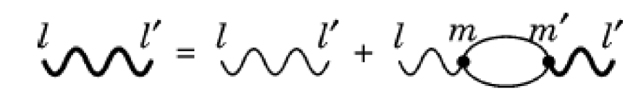
The incident electron beam and electromagnetic field, which act on the layered graphene-related systems, will be dynamically screened by conduction and valence electrons, or will have strong interactions between the external perturbations and the charge carriers. During the complicated screening processes, they create the excited electrons (holes) above (below) the Fermi level. Such intermediate states could further decay by the inelastic electron-electron and electron-phonon scatterings. At low temperature, we only focus on the former mechanisms. The Coulomb decay rate () is fully determined by the effective interaction potential () between two charge carriers, in which the dynamic e-e interactions could be understood from the layer-dependent modified RPA. By using the Matsubara Green’s functions,[242] of monolayer graphene is calculated from the quasiparticle self-energy, the screened exchange energy (the RPA self-energy as clearly shown in Fig. 2-4)
| (14) |
where , (complex fermion frequency), (complex boson frequency) and is the noninteracting Matsubara Green’s function. is the screened Coulomb interactions with the band-structure effect, in which the intraband and the interband deexcitation channels need to be taken into account simultaneously. is the 2D bare Coulomb potential energy and is the RPA dielectric function. This equation is also suitable for monolayer silicene and germanene under the spin-degenerate states,[325] although they possess the significant spin-orbital couplings. It does not need to solve the spin-up- and spin-down-related Coulomb decay rates separately, since they make the same contributions. That is, it is sufficient in fully exploring the wave-vector-, conduction/valence- and energy-dependent self-energies (Eq. 14).
Under the analytic continuation , the carrier self-energy could be divided the bare exchange energy, line part and residue part:
| (15) |
in which
| (16) |
| (17) |
and
| (18) |
The summation of the line and residue parts is the so-called correlation self-energy. The imaginary part of the residue self-energy determines the Coulomb decay rate, being characterized as
| (19) |
is the deexcitation/decay energy. and are, respectively, the Bose-Einstein and Fermi-Dirac distribution functions. Equation (17) clearly means that an initial state of can be deexcited to all the available states under the Pauli exclusion principle and the conservations of energy and momentum. The excited states above or below the Fermi level respectively, exhibit the electron and hole decay rates (the first and second terms in Eq. (20)). By the detailed derivations, the zero-temperature Coulomb decay rates of the excited electrons and holes are
| (20) |
where is the Fermi energy for a pristine system/an extrinsic system with carrier doping. is the step function that limits the available deexcitation channels. The Coulomb decay rate is double the energy width of a quasi-particle state. Equations (19) and (20) could be generalized to a single-walled carbon nanotube with a cylindrical symmetry.[470]
The layer-projection method could be developed to thoroughly investigate the Coulomb decay rates in few-layer graphene-related systems. Any electronic states are composed of the tight-binding functions localized at the different layers, so that their inelastic Coulomb scatterings are closely related to the effective layer-dependent Coulomb potentials ( s). First, we need to evaluate in Eq. (4) by using the analytic and numerical forms simultaneously. And then, Eq. (20) is directly suitable for studying the decay rates. The various deexcitation channels are similar in the layer-dependent , but they might exhibit the distinct weights. However, the calculations become very heavy even under the tight-biding model. On the other hand, there are only few studies on bilayer graphenes up to now,[274] in which the main decay mechanisms are not clear in the first-principles method because of the numerical resolution.
2.6.2 ARPES measurements on occupied quasi-particle energy widths
ARPES is the most efficient reliable equipment in studying the quasi-particle band dispersions and energy widths for the occupied electronic states within the first Brillouin zone. Their measurements could examine the band-structure calculations by the tight-bindung model and the first-principles method, and the predicted Coulomb decay rates under the screened exchange self-energy. In general, the ARPES chamber is combined with the instruments of sample synthesis to measure the in-situ quasi-particle states. When a specific condensed-matter system is illuminated by the soft X-ray (Fig. 2-5), the occupied valence states are excited to the unoccupied intermediate ones under a electric-dipole perturbation. Photoelectrons are excited by incident photons and escape outside of the material surface into the vacuum, and then they are measured by an angle-resolved (energy,momentum) analyzer. The total momenta of photoelectrons are evaluated from the electron gas model, in which the parallel and perpendicular components depend on the polar and azimuthal angles, as shown in Fig. 2-5 by and , respectively. The former is conserved through the photoemission process, while the conservation law is not reliable for the latter because of the destruction of translation symmetry along the direction normal to surface. As a result, ARPES measurements are mainly focused on two- and quasi-two-dimensional systems with the negligible energy dispersions perpendicular to surface. However, the non-conservation issue might be solved using the important characteristics of the -dependent band structure, as done for the 3D band structure of layered graphite by that at .[111, 112, 113, 114] Specifically, the ARPES measurements could provide energy widths of valence states, directly reflecting the many-particle deexcitation scatterings arising from the electron-electron and electron-phonon interactions. Improvements in energy and momentum resolutions have become a critical factor for studying the emergent low-dimensional materials. Up to date, the best resolutions for energy and angular distribution are, separately, 1 meV and 0.1∘ in the UV region.
The high-resolution ARPES is an only experimental instrument in directly measuring the wave-vector-dependent valence/occupied energy spectra. The experimental measurements have confirmed the geometry-enriched band structures in the graphene-related condensed-matter systems, as verified for various dimensions, layer numbers, stacking symmetries, and adatom/molecule chemisorptions. There exist -dependent 3D band structures of Bernal graphite,[111, 112, 113, 114] 1D parabolic energy subbands in graphene nanoribbons,[157, 158] the linearly isotropic Dirac-cone structure in monolayer graphene,[159, 45] and few-layer AA-stacked graphene,[56, 57] two pairs of parabolic dispersions in AB-stacked bilayer graphene,[66, 65, 67, 68] the coexistent linear and parabolic bands in symmetry-broken bilayer graphene,[160] the linear and parabolic bands in trilayer graphene with ABA stacking,[66, 67, 68] the linear, partially flat and sombrero-shaped bands in ABC-stacked trilayer graphene,[67, 66, 68] the metal-semiconductor transitions and the tunable low-lying energy bands after the molecule/adatom absorptions on graphene surface.[161] On the other side, the predicted Coulomb decay rates could be examined from the high-resolution ARPES measurements on the energy widths, as clearly revealed in potassium chemiadsorption on monolayer graphene. The ARPES energy spectra are done along KM and K directions under various doping concentrations of monolayer electron-doped graphene, obviously indicating the linewidth variation with wave vector. They are further utilized to analyze the doping-dependent momentum distribution curves (MDCs). The Lorentzian peak forms are centered at the quasi-particle energies; furthermore, they exhibit the full width at the half-maximum intensity identified as (just the scattering rate). The single-particle excitation and plasmon modes, as well as the electron-phonon scatterings at finite temperatures, are proposed to comprehend the unusual energy dependences of the MDCs linewidths. The ARPES measurements at low temperatures could provide the Coulomb-scattering-dominated MDCs to verify the theoretical calculations.
In addition to the direct ARPES measurements on the energy widths of the valence quasiparticle states, the lifetimes (the inverse of the former) of the specific states, including the Fermi-momentum states and the excited valence and conduction band-edge states, could be examined by three kinds of pump-probe [also sees Chap. 14.1]. The femtosecond photoelectron spectroscopy is available in fully exploring the carrier relaxation near the Fermi level; that is, it is very suitable for the semimetallic and metallic systems. For example, the measured liftimes, which correspond to the Fermi-momentum states in the Bernal graphite and the metallic single-walled and multiwall carbon nanotubes. are, respectively, ps and 0.2 ps at room temperature.[45, 44, 43, 488, 487, 491, 492] As for the femtosecond optical absorption/transmission/reflectivity and fluorescence spectroscopies, they are designed for the semiconducting systems, such as the type-II narrow-gap and type-III moderate-gap carbon nanotubes. The latter nanotube systems are identified to exhibit the lifetimes of ps and ps, respectively, being associated with the first and second prominent absorption peaks.[493, 477, 478, 479, 480, 481, 493, 483, 484] Such decay rates are attributed to the intraband inelastic Coulomb scatterings The experimental measurements on carbon nanotubes are consistent with the theoretical prdictions.[470] The time- and temperature-dependent photolumence spectra have been made on the very small carbon nanotube in the range of K, revealing the band-edge-state lifetimes due to the first pari of energy bands about ps.[485, 486] Such femtosecond spectroscopies are the critical tools in studying the generation, relaxation, and recombination of the nonequilibrium charge carriers, i.e., they can probe and verify the time-dependent carrier dynamics.
3 Concluding remarks and perspectives
The current book clearly presents a fully modified theory on Coulomb excitations/decays in graphene-related systems, in which the theoretical framework combines the layer-dependent RPA and the generalized tight-binding model. It can deal with a plenty of critical factors related to the different lattice symmetries, layer numbers, dimensions, stacking configurations, orbital hybridizations, intralayer interlayer hopping integrals, spin-orbital couplings, temperatures, electron/hole dopings, electric field, and magnetic field. Apparently, there exist the rich and unique electronic excitation phenomena due to the distinct energy bands and wave functions in the various condensed-matter systems, as obviously revealed in the diverse (momentum, frequency)-phase diagrams. The calculated results, with the concise physical pictures, clearly illustrate the very important roles of the e-e Coulomb interactions. Of course, they could explain the up-to-date experimental measurements. This model could be generalized to the other emergent 2D materials under the detailed calculations/investigations, such as, the layered silicene,[36, 154, 374, 134] germanene,[156, 325] tinene,[465] phosphorene,[31] antimonene,[31] bismuthene,[31, 376] and MoS2.[31] The further studies would provide the significant differences among these systems and be very useful in thoroughly understanding the close/complicated relations of the essential physical properties. On the other hands, the theoretical models should be derived again to solve the Coulomb excitations in 1D and 0D systems without the good spatial translation symmetry.[128, 126, 128, 337, 418, 419, 420] For example, 1D graphene nanoribbons and 0D graphene quantum dots have the open boundary conditions, so that they, respectively, possess many energy subbands and discrete energy levels. Maybe, the dielectric function tensor, being characterized by the subband/level index, is one effective way to see the excitation properties.[398]
The theoretical framework of Coulomb excitations and decay rates have been fully developed in Chap. 2, in which the experimental progresses, respectively, on EELS, IXS and ARPES are investigated in detail. The dielectric functions and the energy loss functions are, respectively, are responsible for the single- and many-particle excitation spectra, They strongly depend on the geometric structure/the translation symmetry, directly affecting the longitudinal transferred momenta. As a result, the 3D graphite, 2D graphene, and 1D carbon nanotubes, respectively, exhibit the dimension-related bare Coulomb interactions. so that such condensed-mattered systems are expected to create the diverse Coulomb excitation phenomena. Specifically, few-layer graphenes possess the tensor forms in the dielectric functions, but not the scalar quantities. The main reason is that the interlayer hopping integrals and the interlayer Coulomb interactions need to be taken into account simultaneously. The straightforward combinations between the modified RPA and the generalized tight-binding model has been made; furthermore, the dimensionless energy loss function, directly corresponding to the measured excitation spectrum, is well-defined and rather reliable. The new theoretical model is very suitable for the composite effects due to the stacking configurations, the number of layers, the various lattice symmetries, the spin-orbital couplings, the electric field, and the magnetic field, especially for the unusual magneto-electronic excitations arising from the magnetic quantization. Also, for the excited quasiparticles in layered graphenes, it is rather reliable in exploring the Coulomb inelastic scattering rates of the excited quasiparticles in layered graphenes by linking the screened exchange energy of the Matsubara,s Green functions. This method could provide the clear and concise physical pictures about the effective deexcitation channels. On the other side, the experimental techniques, the up-to-date resolutions, and the whole measured results are another focuses of diverse excitation phenomena. The detailed comparisons with the theoretical predictions could be found in the following chapters.
Monolayer graphene exhibits the rich and unique Coulomb excitations in the presence/absence of temperature, doping, and interlayer Coulomb coupling. A pristine system is a zero-gap semiconductor, so that the Landau dampings at only coming from the inter--band transitions of the linear Dirac-cone structure are too strong to observe the 2D acoustic plasmon modes. The thermal excitations could create the -dependent free electron/hole density. When temperature is higher than the critical one, the intra--band excitations and the 2D-like plasmons ( 0.1 eV at room temperature) come to exist. Compared with the thermal effects, the carrier doping induces the new/extra single-particle and collective excitations more efficiently. Apparently, the higher free carrier density is responsible for the very prominent asymmetric peaks in the polarization functions and the energy loss ones. The rich (momentum, frequency)-phase diagram covers the intraband e-h excitations, the interband ones, the vacuum regions without any excitations, and the undamped/dampled acoustic plasmon mode, being sensitive to the variation of the Fermi level/the doping density, However, it hardly depends on the electron or hole doping as a result of the almost symmetric Dirac-cone energy spectrum about . In addition to the tight-binding model, the effective-mass approximation is utilized to obtain the analytic formula for the polarization/dielectric function, where the conservation of particle numbers needs to be carefully solved during the detailed derivation. It should be noticed that the significant differences between a doped monolayer graphene and a 2D electron gas, directly reflecting the conduction valence Dirac cones and the parabolic conduction band, include the distinct boundaries of the intraband excitations, the existence/absence of the interband excitations, the different Landau dampings of the 2D plasmon modes, the stronger momentum-dependence of plasmon frequencies and more rich (momentum, frequency)-phase diagram in the former. Up to now, the 2D plasmon modes are identified in the EELS measurements of alkali-doped graphene systems,[177, 192, 193, 195, 196, 199] while the temperature-induced ones require the further experimental examinations. The Dirac-cone band structure is approximately reliable in a double-layer system with a sufficiently long interlayer distance. The in-phase and out-of-phase collective oscillations, which, respectively, arise from the symmetric and anti-symmetric superpositions of free carriers on the first and second layers, appear in the energy loss spectra. They belong to the optical and acoustic plasmon modes according to the momentum dependences. The superlattice mode, with a Dirac-cone band structure and the significant interlayer Coulomb interactions, are very useful in understanding the excitation and deexcitation spectra in graphite intercalation compounds.[238, 264]
According to the tight-binding model and the first-principles method,[33, 55] the trilayer ABA stacking presents the composite energy bands, being the superposition of the monolayer- and bilayer-like ones. The layer-dependent polarization functions are a Hermitian matrix, in which the there exist four independent components. A pristine system only exhibits the obvious interband e-h excitations and cannot create any plasmon modes, mainly owing to a very low free carrier density and a non-prominent density of states from the first pair of energy bands. The strong effects, which are due to the electron doping, can dramatically alter the boundaries of the single-particle excitations, add the new excitation channels, and induce three kinds of plasmon modes. The first acoustic mode, the second and the third optical ones, respectively, originate from all the intraband excitations, the and interband transitions. The last kind could be observed only for the higher Fermi level crossing the highest conduction band. There exist the diverse -phase diagrams, being sensitive to the doping carrier density, stacking configuration and layer number. From the view point of electronic and optical properties,[33] the ABA-stacked trilayer graphene could be regarded as the superposition of monolayer and bilayer systems under the single-particle schemes. Apparently, it is not suitable for the many-particle e-e Coulomb interactions. That is to say, it is impossible to understand the diverse (momentum, frequency)-phase diagrams of a trilayer system from those of the composite ones, since the different energy bands will have the significant relations during the interband Coulomb scatterings. Of course, the single-particle and collective excitations are getting more complicated in the increment of layer number, in which the cross-over behavior between the 2D layered graphene and the 3D Bernal graphite might be worthy of a systematic investigation.
Tri-layer ABC-stacked graphene has three pairs of unusual energy bands near the Fermi level [detials in Chap. 6.1]; therefore, it exhibits the rich and unique Coulomb excitations. The layer-indexed bare response functions have nine components, but only four independent ones. There are a lot of single-particle channels and five kinds of plasmon modes during the variation of free carrier densities. The latter cover (I) the intraband plasmon related to the transitions, (II) the interband mode associated with the excitations, (III) the interband one arising from the channels, and (IV) (V) the multimode collective excitations under various intraband and interband channels. The complicated relations between the single-particle and collective excitations create the diverse (momentum, frequency)-excitation phase diagrams. The plasmon peaks in the energy loss spectra might decline and even disappear under various Landau dampings. The linear acoustic plasmon is related to the surface states (the partially flat bands at ) in pristine system, while it becomes an square-root acoustic mode at any doping. Specially, all the layer-dependent atomic interactions and Coulomb interactions have been included in polarization function and dielectric function. The predicted results could be examined from the high-resolution electron-energy-loss spectroscopy[220, 219, 218, 215, 217, 216, 213, 214, 215, 42, 190, 191, 192, 193, 194, 195, 196, 197, 198, 199, 200, 201, 202, 203, 204, 205, 172, 179, 178, 177, 176, 175, 174, 173, 167, 165, 166, 164, 163, 162, 37, 40, 39, 168, 169, 170, 171, 41, 180, 187, 181, 182, 183, 184, 185, 186, 188, 189, 206, 207, 199, 203, 208, 209, 210, 211, 202, 212] and IXS.[224, 223, 225, 226, 227, 228, 229, 230, 231, 232, 233, 234, 172, 235] The magneto-electronic Coulomb excitations in ABC-stacked few-layer graphene systems are expected to the new magnetoplasmon modes because of the frequent-anti-crossing LLs.[318] Moreover, the theoretical framework of the layer-based RPA could be further generalized to study the e-e interactions in emergent 2D materials, e.g., ABC-stacked trilayer silicene and germanene.[36, 156]
Apparently, the trilayer AAB stacking exhibit the unique electronic properties and thus the diverse Coulomb excitations. The lower stacking symmetry leads to three pairs of unusual energy dispersions: the oscillatory, sombrero-shaped, and parabolic ones. The former two possess the large and special van Hove singularities, especially for the first pair nearest to the Fermi level. As a result, for the pristine system, there exist nine categories of valenceconduction interband transitions. The special structures in the bare response functions cover the square-root asymmetric peaks and the shoulder structures [the pairs of anti-symmetric prominent peaks and logarithmically symmetric peaks] in the imaginary [real] part. The threshold channel, , can create the significant single-particle excitations and the strong collective excitations. The low-frequency acoustic plasmon, being characterized by the pronounced peak in the energy loss spectrum, is purely due to the large DOS in the oscillatory valence and conduction bands and the narrow energy gap; furthermore, its intensity and frequency is somewhat reduced by the finite temperatures. The similar plasmon mode is revealed in a narrow-gap carbon nanotube.[337] The critical mechanism about the creation of this plasmon is thoroughly transformed into all the intraband conduction-band excitations, in which the effective channels and the critical transferred momenta strongly depend on the Fermi level. After the electron/hole doping, the interband e-h excitation regions are drastically modified and the extra intraband ones are generated during the variation of . Moreover, one or two higher-frequency optical plasmon modes survive under the various Fermi levels. They are closely related to the specific excitation channels or the strongly overlapped multi-channels, being sensitive to the Fermi level and transferred momenta. There are certain important differences among the trilayer AAB, ABC, ABA and AAA stackings, such as, the boundaries of the various intraband and interband e-h excitations, and the mechanism, number, strength, frequency and mode of the collective excitations. To fully explore the geometry-enriched Coulomb excitations, the above-mentioned theoretical predictions require the experimental verifications.
The sliding bilayer graphene systems obviously exhibit the stacking-configuration- and doping-enriched Coulomb excitation phenomena, mainly owing to the unique essential properties. The shift-dependent characteristics of electronic properties cover the two distinct Dirac cones with the non-titled/titled axis, the normal parabolic bands, the highly hybridized/distorted energy dispersions, the stateless arc-shaped regions, the Dirac points, the local minima/maxima, the saddle points, the Fermi-momentum states, and the symmetric anti-symmetric/the abnormal superposition of the subenvelope functions on the equivalent/non-equivalent sublattices. The available excitation channels are classified into the intrapair intraband, interpair, and intrapair interband transitions, strongly depend on the relative shift of two graphene layers. Under the small transferred momenta, they, respectively, appear at very low frequency, eV eV, and eV. The former two channels are very sensitive to the free carrier doping; that is, they might come to exist, or be partially/fully suppressed under the rigid shift of the Fermi level. The last one hardly depends on . The single-particle excitations, which are associated with the band-edge and Fermi-momentum states, create the special structures in the polarization functions. The abnormal imaginary/real parts present in the square-root asymmetric peaks, the shoulders/the logarithmically symmetric peaks, and the inverse structures of the second types. They, respectively, arise from the Fermi momenta with the linear energy dispersions, the extremal states of the parabolic bands, and the saddle points. Such prominent single-particle responses are responsible for the serious Landau dampings. Also, both Fermi momenta and band-edge states determine the various electron-hole boundaries, where, the latter correspond to the higher-frequency regions. As to the collective excitations, the acoustic and optical plasmons might exist simultaneously, only one mode survives, or both of them are absent, strongly relying on the relative shift and the free carrier density. The single- and many-particle excitations keep the similar behaviors under a small relative shift of two graphene layers. The [ ]/[, ]/[, ] bilayer stackings are similar to each other, while these three sets sharply contrast with one another. The plasmon modes are most easy to be observed in the first set, and the opposite is true for the third set.
A uniform perpendicular electric field has created the significant effects on the electronic properties and thus diversifies the Coulomb excitation phenomena. The essential properties, which over the Dirac points, the Fermi velocity, the Fermi momenta, the valence and conduction band overlap/the free electron and hole densities, the band gap, the band-edge states with large DOSs, the energy dispersions, the symmetric antisymmetric linear superposition of the tight-binding functions, and the equivalence of the layer-dependent A and B sublattices, clearly display the drastic changes or the dramatic transformations under the layer-related Coulomb potential on-site energies. This field is further responsible for the unusual single-particle and collective excitations in layered graphene systems. Apparently, the AA-, AB-, and ABC-stacked few-layer graphenes exhibit the diverse excitation behaviors. For the -layer AA stackings, there is two/one acoustic plasmon modes in the presence/absence of the electric field. The higher- and lower-frequency modes, respectively, come from all the free carriers (the intrapair intraband transitions) and the -induced band disparity, so that the former behaves like that in a 2D electron gas, and the latter comes to exist only under the significant splitting of the intrapair intraband and interband transitions at the enough large ,s. More optical plasmon modes is revealed in the energy loss spectrum except for the bilayer stacking, compared with the modes in the pristine system. Such optical plasmons mainly arise from the interpair interband channels; furthermore, the extra modes are associated with the nonuniform Fermi velocities and energy spacings between the different Dirac points. Specifically, the AA bilayer stacking can clearly illustrate the concise physical mechanisms by analytically evaluating the electric-field-dependent band structure, wave functions, bare polarization functions (intrapair and interpair parts), and dielectric function matrix. For example, the vanishing determinant of the last one is very useful in understanding the plasmon-frequency dispersion relations with the transferred momentum. Apparently, the -induced electronic excitations are very sensitive to the stacking configurations. The significant differences among the trilayer AAA, ABA and ABC stackings lie in the main features of electron properties, the available transition channels, the singular structures in bare polarization functions; the e-h excitation boundaries and the plasmon modes in the - -phase diagrams. During the variation of , three pairs of vertical Dirac-cone structures remain similar in the AAA stacking, while the others present the strongly oscillatory energy dispersions, especially for the first pair of valence and conduction bands. Most important, the semimetal-semiconductor transition is only revealed under the specific ABC stacking. The observable single-particle transition channels, which correspond to the AAA-, ABA- and ABC-stacked systems, are, respectively, divided into three interband and two intraband excitation categories, five interband excitation categories, and four ones. Furthermore, such bare polarization functions, being associated with the band-edge states, display the square-root divergent peaks and the shoulder asymmetric peaks (composite structures of shoulders and logarithmically divergent peaks) in the AAA and [ABA, ABC] stackings. The most prominent plasmon, respectively, behaves the acoustic and optical modes for the [AAA, ABA] and ABC stackings. The mechanism is different between AAA and [ABA, ABC] stackings, since this mode mainly originate from the first third pairs of Dirac cones and the first pair of valence and conduction bands. Within a certain range of , there co-exist the splitting modes, in which the number is, respectively, two, two and three. As to the higher-frequency optical plasmons, it is relatively easy to observe them in the trilayer AAA stacking because of three splitting modes. However, only one mode appears in the ABA and ABC systems.
The entire LL energy spectrum is included in the calculations. This ensures the correctness of the dielectric function within the RPA and consequently the energy loss function, and the intensity and frequency of magnetoplasmon modes. The exact diagonalization method in efficiently solving the LL wavefunctions and the Coulomb matrix elements could also be applicable to multilayer graphene or bulk graphite over a wide range of magnetic and electric fields. As to monolayer graphene, there are a lot of observable and weak magneto-plasmon peaks, being sensitive to the strength of the e-h dampings. Their frequencies present the unusual -dependence, in which the critical transferred momentum directly reflects the rather strong competition between the longitudinal Coulomb forces and the transverse cyclotron ones. The positive and negative group velocities, which, respectively, occur at and , corresponds to the dominance of the former and the latter. and the magnetoplasmon frequencies grows with the magnetic field, especially for . Temperature effectively induce certain low-lying intraband excitations due to the conduction/valence LLs. The intraband magnetoplasmons would come to exist only under the sufficiently high temperature, in which the critical temperature grows with the increasing magnetic-field strength. The magneto-Coulomb excitations are greatly diversified by the stacking configurations. The low-energy excitations in the bilayer AB/AA stacking are only created by the interband/intrabands of the intragroup inter-LL channels. This directly reflects the spatial symmetric or anti-symmetric distributions on four sublattices of the magnetic LL wave functions, as observed in zero-field cases. The former and the latter, respectively, exhibit a lot of and certain prominent peaks in the layer-dependent polarization functions and the energy loss spectra. The discrete magnetoplasmon frequencies of the AB stacking are similar to those in monolayer graphene, while they present more complicated momentum-dependence. The critical momenta and the serious Landau dampings are responsible for the discontinuous but monotonous -dependence. Specially, the 2D-like plasmon, accompanied with some discrete modes, appears in the AA stacking, clearly illustrating free holes/electrons in the unoccupied valence LLs of the first group/the occupied conduction ones of the second group. The dramatic variation of the highest occupied LL leads to the discontinuous and oscillatory -dependence. Moreover, the significant differences between the Coulomb and EM wave perturbations clearly indicate the diverse magenta-electronic excitation phenomena.
Apparently, the 3D three kinds of graphites show the diverse Coulomb excitation phenomena in the low- and middle-frequency ranges, mainly owing to the dimensionality and stacking configurations. That is, the single-particle and collective excitation fully reflect the main features of band structures, the strong wave-vector dependence, the highly anisotropic behavior, the special symmetry, and the 3D dimensional band overlap. Among the well-stacked graphites, the simple hexagonal (rhombohedral) graphite possesses the higher (lower) geometric symmetry, the largest (smallest) energy width along , the strongest (weakest) band overlap, and the heaviest (lightest) free electron and hole densities. The unusual geometric and electronic properties are responsible for the unique electronic excitations. As to the AA-stacked graphite, both low-frequency e-h excitations and plasmon modes could survive for any directions of transferred momenta, in which the optical modes are similar to those in a 3D electron gas. The significant differences between the parallel and perpendicular transferred momenta cover the higher plasmon frequency, the lower peak intensity, and the smaller critical momentum under the former case. It is relatively easy to observe the low-frequency optical plasmons in the perpendicular case because of the almost vanishing inter--band e-h excitations. On the other hand, both AB- and ABC-stacked graphite display the low-frequency optical plasmons only for the perpendicular transferred momenta, in which the dispersion relations with are weak. Their low-frequency excitations are strongly affected by temperature because of very low free carrier densities, especially for the existence of the optical plasmons in the latter. The predicted -dependent plasmon frequencies in Bernal graphite are roughly consistent with those measured by the high-resolution EELS [40, 392, 394, 393, 175, 39, 174, 224] and optical reflectance spectroscopy.[395, 392, 394, 393] Doping in the AA-stacked graphite leads to drastic changes in the -electronic excitations, such as, the great enhancement of plasmon frequency and strength. The theoretical predictions could account for the EELS and optical measurements on the optical plasmons in LiC6.[178, 179] The simple hexagonal graphite sharply contrasts with a monolayer graphene in terms of the low- and middle-frequency excitation channels. For example, concerning graphene system, the low-frequency plasmon modes are absent for the pristine case and . They are created by the doping or finite temperatures, but their behaviors at long wave length limit belong to the acoustic modes. Moreover, the -plasmon frequency of graphene is much lower than those of the 3D systems at small transferred momenta, owing to the lower and narrower saddle-point DOS, and the weaker Coulomb interactions at small momenta. Specifically, the diversified plasmons are revealed in three kinds of graphites, in which the main features, the existence, intensity and frequency, depend on the direction and magnitude of the 3D transferred momenta, and the stacking configurations. The plasmons, the collective oscillation mode of the whole valence electrons, are present under any parallel momenta, while those for the perpendicular momenta are present only at the sufficiently large parallel components. The dependences on and , respectively, grow rapidly and decline slowly in the increment of momentum. The azimuthal anisotropy comes to exist when is enough high. The predicted -plasmon frequencies for the -component approximately agree with the EELS measured results on Bernal graphite.[40, 392, 394, 393, 175, 39, 174, 224] In addition, a simple superlattice model is also utilized to explain the significant features of the -electronic collective excitations. Apparently, such plasmons are revealed in the -bonding carbon-based materials, but regardless of the and bondings. There exist certain important differences among graphites,[27, 39, 40] layered graphenes, [24, 42, 29] carbon nanotubes, [19, 50, 126, 128, 180, 181, 183, 184] and C60-related fullerenes[218], such as, the momentum- and angular-momentum-decoupled collective oscillation modes.
The 1D carbon nanotubes have the rich electronic properties and many-particle excitation phenomena, being sensitive the changes in the transferred momenta and angular moments (), nanotube geometry (radii chiral angles), temperatures, doping levels, and magnitudes directions of the magnetic fields. There are three types of carbon nanotubes under the curvature effects according to the concise rule: (1) type-I metals for (armchair), (2) type-II narrow-gap systems for , and (3) type-III moderate-gap ones for . Only the first type exhibits the low-frequency acoustic plasmon with the specific dependence at small momenta. Such plasmon comes from the interband excitations of a pair of linearly intersecting valence and conduction bands near the Fermi level. This plasmon mode hardly depends on finite temperatures, while the sufficiently high s can create the intraband low-frequency plasmon in a narrow-gap large carbon nanotube and a zero-gap semiconducting monolayer graphene. The free carriers can induce a low-frequency intraband plasmon of in all the carbon nanotubes. Furthermore, the high-level doping even leads to the creation of the optical plasmon mode. As to the magnetic field, its strong effects are to drastically/dramatically alter the energy dispersions band gaps of electronic structures and the wavefunctions, mainly arising from the obvious variation of and the coupling of distinct ,s. The former mechanism induces the periodical Aharnov-Bohm effect under the negligible Zeeman splittings, and the latter one results in the irregular standing waves on a cylindrical surface. Each armchair nanotube only shows one magnetoplasmon mode due to the interband excitations under the non-perpendicular magnetic field. However, the low-frequency magnetoplasmon becomes the composite intraband and interband mode at or high ,s. The nonarmchair narrow-gap .nanotubes exhibit two magnetoplasmon, while the nonarmchair metallic nanotubes present one interband magnetoplasmon and one interband intraband magnetoplasmom. The Zeeman splitting plays an important role on the significant differences among these magnetoplasmon modes. In addition to the low-frequency -electronic excitations, there exist the inter- band and plasmons in various carbon nanotubes, in which they, respectively, corresponds to the specific valence bands and the whole -valence electrons. Their dependence on angular momentum, radius and chiral angle is significant, while the momentum dispersion relation might be strong or weak. Among three types of nanotube systems, armchair/zigzag ones have the smallest/largest mode number of inter--band plasmons. The -plasmon frequencies of eV, which grow with the increasing , are very suitable in identifying the intrinsic -decoupled modes of the cylindrical systems. Up to now, the higher-frequency inter--band and plamsons have been confirmed by the accurate EELS measurements.[180, 181, 182, 183, 184, 185, 186] However, the low-frequency ones, being due to the geometry, temperature, magnetic field and doping, require the further experimental verifications. Apparently, the Coulomb excitation phenomena are greatly diversified by the 1D cylindrical surface and the 2D plane (the different geometric symmetries). The distinct bare Coulomb interactions and electronic properties can create the sharp differences for carbon nanotubes and layered graphenes, covering the conserved quantities in the electron-electron scatterings, the existence/absence of the low-frequency plasmons, and the composite effects coming from the critical factors (temperature, strength and direction of magnetic field, and doping density).
Obviously, group-IV monolayer systems exhibits the rich and unique Coulomb excitation spectra, in which there are certain important differences among silicene, germanene and graphene. For pristine systems, the near-neighboring hopping integral, spin-orbital coupling and temperature play the critical roles in creating the available single-particle transitions and the observable plasmon modes. The first and second factors are, respectively, responsible for and gap and Fermi velocity; therefore, they co-determine the critical temperature and the threshold excitation frequency. When the temperature is sufficiently high, the -induced intraband transitions will strongly suppress and even replace the original interband ones. The intraband and interband e-h excitations, respectively, display the square-root divergent peak and shoulder structure in the imaginary part of dielectric function. There are three types of collective excitations, as clearly illustrated from phase diagrams under the specific temperatures. For example, silicene, with a very narrow gap, shows (I) the undamped plasmon between the intraband and interband boundaries, (II) the similar one and another weaker plasmon and (III) the undamped and damped plasmon, in which the first and third kinds of plasmon modes (the second kind) experiences the interband (intraband) Landau dampings. The diverse behaviors strongly depend on the range of temperature: (I) 75 K, (II) 75 K K and (III) K. The electric field in a buckled system can destroy the mirror symmetry about the plane and create the splitting of spin-up and spin-down energy bands, resulting in the diversified Coulomb excitation phenomena in the -, - and -phase diagrams. They clearly present the different critical momenta, temperature and electric-field strengths under the various cases, indicating the dramatic changes of the intensities of energy loss functions and thus the emergence/disappearance of plasmon mode and the significant Landau dampings. Furthermore, four types of single-particle and collective excitations, which depend on the specific and , are characterized by: (I) the excitation gap exists between the intraband and interband transitions of the spin-degenerate valence and conduction bands (without ), and an intraband plasmon is undamped at small ,s and then disappears at large ,s because of the serious Landau dampins near the intraband boundary. (II) three e-h boundaries, the lower, middle and upper ones, are induced by the intraband transitions from the spin-down-dominated energy bands, the interband transitions of the same pair, and the interband transitions due to the spin-up-dominated pair. The most prominent intraband plasmon survives between the former two boundaries. It experiences the interband e-h damping near the middle boundary, accompanies with another weaker plasmon. This mode is absent at large ,s under the intraband dampings (close to the lower boundary). (III) the merged intraband and interband boundaries related to the linear energy bands intersecting at and the higher-frequency interband boundary associated with the spin-up-dominated energy bands. The intraband plasmon has a strong e-h dampings even at long wavelength limit. (IV) The e-h boundaries are the same with those in (II), while this plasmon is undamped only near , and then it enters into the distinct interband Landau dampings related to the first and second pairs of spin-split energy bands. Concerning the complex composite effects arising from the spin-orbital interactions, magnetic field, electric field, and electron doping, they further diversify the single-particle and collective excitations. The magnetic field creates the interband magnetoplasmons with discrete frequency dispersions restricted to the quantized LL states. An intraband magneoplasmon, with a higher intensity and continuous dispersion relation, comes to exist in the presence of free conduction carriers. This mode is dramatically transformed into an interband plasma excitation when the magnetic field is increased, leading to abrupt changes in plasma frequency and intensity. Specifically, an electric field could separate the spin and valley polarizations and induce additional magnetoplasmon modes, an unique feature arising from the buckled structure and the existence of the significant spin-orbit couplings. The intraband and interband magnetoplasmons, respectively, belong to the continuous and localized modes. In short, it is relatively easy to observe the split valleys and spin configurations in monolayer germanene, since it has the largest spin-orbital couplings among three group-IV systems (C, Si; Ge).
Apparently, monolayer graphene presents the rich and unique Coulomb deexcitation phenomena, being very different from 2D electron gas, 1D carbon nanotubes, silicene, and germanene. The inelastic Coulomb scatterings could be investigated from the screened exchange self-energy method and the Fermi golden rule. Concerning the Coulomb decay rates in pristine graphene, they directly reflect the characteristics of band structure, the zero-gap semiconductor and the strong dependence on wave vector/state energy. At = 0, only the interband e-h excitations exist, and their contributions to the Coulomb decay rates are negligible. The temperature-induced free carriers create the intraband e-h excitations and the acoustic plasmon. The strength of plasmon mode grows (declines) as temperature (momentum) increases. The Coulomb inelastic scatterings of the Fermi-momentum state (the Dirac point) only utilize the intraband e-h excitations, with any transferred momenta, leading to the non-specific -dependence. The calculated decay rate is close to the measured results of the layered graphite.[274, 472] The intraband e-h excitations also make important contributions to other states. Both interband e-h excitations and plasmon belong to the critical deexcitation channels for the small- states. They, respectively, result in the special shoulder and peak structures in the wave-vector-dependent decay rates of the conduction- and valence-band states. The e-e interactions are more efficient in carrier deexcitations, compared with the electron-phonon interactions. The important differences between graphene and 2D electron gas lie in the temperature and wave-vector dependences, since the the band structure of the latter can only generate the intraband e-h excitations and its acoustic plasmon survives even at . The plasmon is not the effective deexcitation channel and the small- intraband e-h excitations predominate over the relaxation process, so that the temperature- and energy-dependent Coulomb decay rates could be expressed in the analytic formulas.[274] The absence of the specific formulas in monolayer graphene clearly indicates that the large-() intraband e-h excitations, the plasmon, and the interband e-h excitations are not negligible in the inelastic Coulomb scatterings. These three kinds of electronic excitations are expected to play an important role on the low-energy quasiparticle properties of few-layer graphene systems. There also exist significant differences between 2D graphene and 1D gapless carbon nanotubes, covering the magnitude, temperature-dependence and wave-vector-dependence of the Coulomb decay rates. The Dirac point in armchair nanotube shows the linear -dependence, as observed in a 1D electron gas.[242] Apparently, the Coulomb decay rates of monolayer graphene are greatly diversified by the electron (or hole) doping. The deexcitation processes cover the intraband single-particle excitations, the interband e-h excitations, and the damped or undamped collective excitations. depending on the quasiparticle states and the Fermi energies. The low-lying valence holes can decay through the undamped collective excitations; therefore, they present the fast Coulomb deexcitations, nonmonotonous energy dependence, and anisotropic behavior. However, the low-energy conduction electrons and holes are similar to those in a two-dimensional electron gas. In addition, the Fermi-momentum states display the dependence. The higher-energy conduction states and the deeper-energy valence ones behave similarly in the available deexcitation channels and have a strong dependence on the wave vector , since the contributions due to intraband (interband) e-h excitations quite differ from one another along the distinct directions. Moreover, there exist the significant differences among the extrinsic graphene, silicene and germanene in terms of the available deexcitation channels and certain Coulomb decay phenomena. Specially, a doped germanene shows the composite effects due to the spin-orbital couplings and electron doping. The second and third kinds of plasmon modes might be the effective Coulomb scattering channels. Moreover, the deexcitation mechanisms sharply contrast for the separated valence and conduction Dirac points, in which the former could decay by the acoustic plasmon and thus has the faster Coulomb decay rate.
The generalized tight-binding model and the modified RPA are developed to deal with the Coulomb excitations and decay rates under various stacking configurations, layer numbers, dimensionalities, electric fields and magnetic fields. The bare and screened response functions are thoroughly clarified by using the dynamically electron-electron inelastic scatterings. Specifically, the latter is very useful in the further understanding of the time-dependent carrier oscillation/propagation in the real graphene-related systems. These energy loss spectra are very sensitive to the magnitude and direction of the transferred momenta under various frequencies. From the theoretical point of view, one must preform the 3D Fourier transform for them to explore the time- and position-dependent collective oscillation phenomena accompanied with the Landau dampings. The calculated results in Chaps. 3-14 clearly show that there are three kinds of plasmon modes due to the carbon orbitals in graphene-related -bonding systems. The and inter--band plasmons possess the oscillational frequencies more than 1 eV, corresponding to a very rapid oscillation/propagation with a period below 4 fs. Apparently, the time resolution is too high for the up-to-date femtosecond optical spectroscopies; that is, it is impossible to observe and identify the oscillation behaviors from these two kinds of plasmon modes using the current high-resolution equipments. On the other hand, the low-frequency plasmon modes, with the different momentum dispersions, are expected to reveal in all the graphene-related materials. For example, the -meV plasmon modes, with oscillation periods fs, are very suitable for the experimental verifications on the diverse plasmon waves accompanied with the various Landau dampings. Such collective excitations are deduced to originate from the temperatures, lattice symmetry, dimensionalities, stacking configurations, numbers of layers, spin-orbital interactions, electric fields, and magnetic fields. That is to say, a lot of critical mechanisms could also be illustrated by the dynamic behavior of the excited carriers. The time-dependent charge oscillations/propagations in the layered structures will become an interesting and emergent research topic; furthermore, the dynamics of plasmon modes might have high potentials in electronic and optical devices.[425, 45] Such work is under current investigation.
The above-mentioned two models are very useful in fully exploring the static charge screening of graphene-related systems, especially for the spatial variations (distributions) of the effective Coulomb potentials and the induced carrier density on the distinct planes. The momentum- and frequency-dependent Coulomb potentials, which have been thoroughly investigated in the current work for the 1D, 2D and 3D -bonding systems, could be recovered to the static effective Coulomb interactions in the real space by doing the Fourier transform at zero frequency. The similar method is applied to the induced charge density (the product of the effective potential and the bare response function in the momentum space). The free carrier density and the Fermi surface (the Fermi momenta), or the energy gap are expected to play critical roles on the unusual screening behaviors. Whether the long-range effective Coulomb interactions decay quicker than the inverse of distance is the standard criteria for the charge screening ability. The semiconducting carbon nanotubes have been predicted to exhibit the long-distance Coulomb potential similar to the bare one.[127] However, the metallic armchair nanotubes[128], layered graphenes[518] and graphite intercalation compounds[502] obviously display the exponential decay at the short distance and the well-known Friedel oscillations at the long distance. The characteristic decay length and the rapid charge oscillations are very sensitive to the concentration of free carriers and the spatial dimensions. From the theoretical point of view, the strong Friedel oscillations mainly come from the divergent derivative of the static bare response functions versus the transferred momentum at the double of Fermi momentum, as identified from 3D and 2D electron gases.[242] On the other hand, STM has been demonstrated to be a powerful tool for visualizing the Friedel oscillations in real space of 2D graphene-related systems in response to the atomic-scale impurities.[519] In general, both pristine few-layer graphene systems and 3D graphites, which belong to the semi-metals, are expected to show the marginal (partial) screening ability in between the full and almost vanishing ones. Also, the doped layered graphene systems, with the distinct stacking configurations and layer numbers, are very suitable for exploring the diversified charge screening phenomena, e.g., the theoretical[268, 271, 324, 353, 240, 249, 267, 24, 127] and experimental studies on the 2D Friedel charge oscillations.[66, 159, 155] In addition, the effective Coulomb potentials due to the charged impurities could investigate the residual resistivities in layered materials, e.g., the zero-temperature elastic scatterings for the residual resitivies in alkali-doped graphite compounds.[502]
The Friedel oscillations can be studied with the use of the static dielectric screening in the generalized tight-binding model. In a monolayer graphene, the static dielectric function is calculated by specifying the general results of the full charge screening due to the massless-Dirac quasiparticle, which is incorporated by the development of the modified random-phase approximation (RPA), summarized in Chap. 2. As shown in Fig. 14-11, the induced charge distribution and the screened potential are presented for the static case of a charge impurity at in the doped graphene under various Fermi levels. The most outstanding feature of the Friedel oscillations is the strong oscillation behaviour in real space, a phenomenon being deduce from a discontinuity of the second derivative of the static dielectric function. At higher dopings, the screening charges become rather extended in r-space, with a long-wavelength decay of oscillations at a distance from the impurity.[518] It should be noticed that there is no interband contribution from the long-wavelength behaviour of the polarization since the corresponding polarization approaches zero at . This indicates that the non-oscillating part at small-r distances comes from the intraband polarization with a characteristic decaying length that can be evaluated within the Thomas-Fermi approximation. The previous work has indicated that as is increased the interband transitions greatly enhance the large- screening as compared to the intraband transitions, and consequently make the small- screening effects rather effective from an impurity.[502] However, and very importantly, at a long distance from the impurity, the decaying oscillation behaviour with a unique period given by comes from the discontinuity at as a result of the singularities in the second derivative of the static dielectric function. The aforementioned features are expected to have important influences on, for example, the ordering of impurities and the resistivity in graphene-related systems.[502]
The dimensionless energy loss function, which characterizes the intrinsic charge screeing of a layered condensed-matter system, is well developed in this work. Furthermore, the modified RPA [Chap. 2.1] is very suitable and reliable in evaluating the effective Coulomb potentials for the intralayer and interlayer many-particle interactions. As a result, such potentials could be directly linked with the self-energy method of the Matibara Green functions [Chap. 2.6]. The decay rate, being associated with the e-e Coulomb inelastic scatterings on all the graphene layers, could be derived and even expressed in the analytic form. The phenomenological formulas will be investigated fully and delicately. The effects arising from the number of layers and stacking configurations are taken into consideration simultaneously. The rich and unique deexcitation phenomena are expected to reveal in few-layer graphene systems, and they need to be thoroughly explored within this new theoretical framework. For example, the AAA-/ABA-/ABC-stacked -layer graphenes are present in an electromagnetic field, the excited conduction electrons and valence holes in pairs of energy bands will relax through the effective Coulomb excitation channels. The numerical calculations become very difficult, since the anisotropic muti-dimensional integrations appear in the band structure, polarization functions, and transferred momenta and energies. Some efficient methods need to be introduced to overcome the serious issues. On the experimental side, the femtosecond pump-probe optical spectroscopies of absorption and fluorescence are available to identify the diverse deexcition phenomena in few-layer graphene systems. Apparently, such studies could be generalized to the other emergent 2D materials. In short, the near-future researches on the femtosecond dynamics of charge carriers are predicted to open a new studying category.
In addition to the Coulomb scatterings, the electron-phonon scatterings at finite temperatures might play important roles in the electron-electron effective interactions and thus have a strong effect electronic excitation spectra and quasiparticle lifetimes. These two kinds of inelastic scatterings could be taken into account simultaneously under the random-phase approximation of the same order, as clearly illustrated in Refs.[242]. This method has been clearly verified to be suitable and reliable for the doped GaAs semiconductor by measuring the plasmon branches using the Raman scattering.[503] Apparently, the combination of the longitudinal plasmon modes and optical phonons creates the well-known anti-crossing phenomenon in the spectrum of the collective oscillation frequencies. In the near-future studies on few-layer graphene systems, the couplings of acoustic plasmons and longitudinal optical phonons are expected to diversify the (momentum, frequency)-phase diagraoms and greatly modify the inelastic scattering rates of the excited quasiparticle states.[505, 506, 504, 507] On the other side, certain physical barriers in theoretical models need to be overcome, such as, the delicate phonon spectra of layered graphenes calculated by the oscillator model,[508, 509] the effective amplitude of the electron-phonon scatterings using the phenomenological method,[510, 511, 512] the modifications of the layer-dependent random-phase approximation,[513] and the modified screened exchange energies.[514] They will become challenges and chances for a full understanding of the overall quasipaticle phenomena in 2D emergent materials. For example, there are some theoretical predictions on phonon spectra, especially for the first-principles calculations,[517, 515, 516] in which how to transform the evaluated results into the very useful information in establishing the electron-phonon scattering amplitudes is one of the high barriers.
Acknowledgments
This work was supported in part by the National Science Council of Taiwan, the Republic of China, under Grant Nos. NSC 98-2112-M-006-013-MY4 and NSC 99-2112-M-165-001-MY3.
References
- [1] K. S. Novoselov, A. K. Geim, S. V. Morozov, D. Jiang, Y. Zhang, S. V. Dubonos, I. V. Grigorieva, and A. A. Firsov, Electric field effect in atomically thin carbon film, Science. 306, 666, 2004.
- [2] A. H. Castro Neto, F. Guinea, N. M. R. Peres, K. S. Novoselov, and A. K. Geim, The electronic properties of graphene. Rev. Mod. Phys. 81. 109, 2009.
- [3] A. C. Ferrari, J. C. Meyer, V. Scardaci, C. Casiraghi, M. Lazzeri, F. Mauri, S. Piscanec, D. Jiang, K. S. Novoselov, S. Roth, and A. K. Geim, Raman spectrum of graphene and graphene layers, Phys. Rev. Lett. 97, 187401, 2006.
- [4] Y. Shao, J. Wang, H. Wu, J. Liu, I. A. Aksay, and Y. Lin, Graphene based electrochemical sensors and biosensors: A review, Electroanalysis 22, 1027, 2010.
- [5] Y. Zhang, L. Zhang, and C. Zhou, Review of chemical vapor deposition of graphene and related applications, Acc. Chem. Res. 46, 2329, 2013.
- [6] Y. Wang, Y. Shao, D. W. Matson, J. Li, and Y. Lin, Nitrogen-doped graphene and its application in electrochemical biosensing, ACS Nano 4, 1790, 2010.
- [7] Y. Wang, Y. Li, L. Tang, J. Lu, and J. Li, Application of graphene-modified electrode for selective detection of dopamine, Electrochem. Commun. 11, 889, 2000.
- [8] Z. Fan, J. Yan, L. Zhi, Q. Zhang, T. Wei, J. Feng, M. Zhang, W. Qian, and F. Wei, A three-dimensional carbon nanotube/graphene sandwich and its application as electrode in supercapacitors, Adv. Mater. 22, 3723, 2010.
- [9] A. L. M. Reddy, A. Srivastava, S. R. Gowda, H. Gullapalli, M. Dubey, and P. M. Ajayan, Synthesis of nitrogen-doped graphene films for lithium battery application, ACS Nano, 4, 6337, 2010.
- [10] H. G. Yan, X. S. Li, B. Chandra, G. Tulevski, Y. Q. Wu, M. Freitag, W. J. Zhu, P. Avouris, and F. N. Xia, Tunable infrared plasmonic devices using graphene/insulator stacks, Nat. Nanotechnol. 7, 330, 2012.
- [11] H. G. Yan, T. Low, W. J. Zhu, Y. Q. Wu, M. Freitag, X. S. Li, F. Guinea, P. Avouris, and F. N. Xia, Damping pathways of mid-infrared plasmons in graphene nanostructures, Nat. Photonics 7, 394, 2013.
- [12] T. Low, and P. Avouris, Graphene plasmonics for terahertz to mid-infrared applications, ACS Nano 8, 1086, 2014.
- [13] Y. C. Fan, N. H. Shen, T. Koschny, and C. M. Soukoulis, Tunable terahertz meta-surface with graphene cut-wires, ACS Photonics 2, 151, 2015.
- [14] Y. C. Fan, N. H. Shen, F. L. Zhang, Q. Zhao, Z. Y. Wei, P. Zhang, J. J. Dong, Q. H. Fu, H. Q. Li, and C. M. Soukoulis, Electrically tunable slow light using graphene metamaterials, ACS Photonics 5, 1612, 2018.
- [15] M. J. Allen, V. C. Tung, and R. B. Kaner, Honeycomb carbon: A review of graphene, Chem. Rev. 110, 132, 2010.
- [16] H. Wang, T. Maiyalagan, and X. Wang, Review on recent progress in nitrogen-doped graphene: synthesis, characterization, and its potential applications, ACS Catal. 2, 781, 2012.
- [17] E. McCann, and M. Koshino, The electronic properties of bilayer graphene, Rep. Prog. Phys. 76, 056503, 2013.
- [18] K. W. -K. Shung, Lifetime effects in low-stage intercalated graphite systems, Phys. Rev. B 34, 2, 1986.
- [19] M. F. Lin, and D. S. Chuu, Elementary excitations in a carbon nanotube, J. Phys. Soc. Jpn. 66, 757, 1997.
- [20] Y. C. Chuang, J. Y. Wu, M. F. Lin, Dynamical conductivity and zero-mode anomaly in honeycomb lattices, J. Phys. Soc. Jpn. 71, 1318, 2002.
- [21] Y. C. Chuang, J. Y. Wu, M. F. Lin, Analytical calculations on low-frequency excitations in AA-stacked bilayer graphene, J. Phys. Soc. Jpn. 81, 124713, 2012.
- [22] M. F. Lin, Y. C. Chuang and J. Y. Wu, Electrically tunable plasma excitations in AA-stacked multilayer graphene, Phys. Rev. B 86, 125434, 2012.
- [23] Y. C. Chuang, J. Y. Wu, M. F. Lin, Electric-field-induced plasmon in AA-stacked bilayer graphene, Ann. Phys. 339, 298, 2013.
- [24] J. H. Ho, C. L. Lu, C. C. Hwang, C. P. Chang and M. F. Lin, Coulomb excitations in AA- and AB-stacked bilayer graphites, Phys. Rev. B 74, 085406, 2006.
- [25] C. P. Chang, Exact solution of the spectrum and magneto-optics of multilayer hexagonal graphene, J. Appl. Phys. 110, 013725, 2011.
- [26] Y. C. Chuang, J. Y. Wu and M. F. Lin, Electric field dependence of excitation spectra in AB-stacked bilayer graphene, Sci. Rep. 3, 1368, 2013.
- [27] J. H. Ho, C. P. Chang, and M. F. Lin, Electronic excitations of the multilayered graphite, Phys. Lett. A 352, 446, 2006.
- [28] Y. C. Chuang, J. Y. Wu, and M. F. Lin, Electric field dependence of excitation spectra in AB-stacked bilayer graphene, Sci. Rep. 3, 1368, 2013.
- [29] C. Y. Lin, M. H. Lee, and M. F. Lin, Coulomb excitations in ABC-stacked trilayer graphene, Phys. Rev. B 98, 041408, 2018.
- [30] C. Y. Lin, T. N. Do, Y. K. Huang, and M. F. Lin, Electronic and optical properties of graphene in magnetic and electric fields, IOP Concise Physics. San Raefel, CA, USA: Morgan Claypool Publishers, 2017.
- [31] S. C. Chen, J. Y. Wu, C. Y. Lin, and M. F. Lin, Theory of magnetoelectric properties of 2D systems, IOP Concise Physics. San Raefel, CA, USA: Morgan Claypool Publishers, 2017.
- [32] C. Y. Lin, J. Y. Wu, Y. J. Ou, Y. H. Chiu and M. F. Lin, Magneto-electronic properties of multilayer graphenes, Phys. Chem. Chem. Phys. 17, 26008, 2015.
- [33] C. Y. Lin, R. B. Chen, Y. H. Ho and M. F. Lin, Electronic and optical properties of graphite-related systems, CRC Press, 2017.
- [34] J. Y. Wu, S. C. Chen, O. Roslyak, G. Gumbs, and M. F. Lin, Plasma excitations in graphene: Their spectral intensity and temperature dependence in magnetic field, ACS Nano 5, 1026, 2011.
- [35] J. Y. Wu, G. Gumbs, and M. F. Lin, Combined effect of stacking and magnetic field on plasmon excitations in bilayer graphene, Phys. Rev. B 89, 165407, 2014.
- [36] J. Y. Wu, S. C. Chen, G. Gumbs, and M. F. Lin, Feature-rich electronic excitations of silicene in external fields, Phys. Rev. B, 94, 205427, 2016.
- [37] R.F. Egerton, Electron energy-loss spectroscopy in the electron microscope, 370, Plenum, New York and London, 1996.
- [38] W. Schülke, Electron dynamics by inelastic x-Ray scattering, Oxford University Press, Oxford, 2007.
- [39] K. Zeppenfeld, Wavelength dependence and spatial dispersion of the dielectric constant in graphite by electron spectroscopy, Opt. Com. 1, 119, 1969.
- [40] K. Zeppenfeld, Nonvertical interband transitions in graphite by intrinsic electron scattering, Z. Phys. 243, 229, 1971.
- [41] C. Kramberger, R. Hambach, C. Giorgetti, M. H. Rummeli, M. Knupfer, J. Fink, B. Buchner, Lucia Reining, E. Einarsson, S. Maruyama, F. Sottile, K. Hannewald, V. Olevano, A. G. Marinopoulos, and T. Pichler, Linear plasmon dispersion in single-wall carbon nanotubes and the collective excitation spectrum of graphene, Phys. Rev. Lett. 100, 196803, 2008.
- [42] P. Wachsmuth, R. Hambach, M. K. Kinyanjui, M. Guzzo, G. Benner, and U. Kaiser, High-energy collective electronic excitations in free-standing single-layer graphene, Phys. Rev. B 88, 075433, 2013.
- [43] T. Valla, J. Camacho, Z.-H. Pan, A. V. Fedorov, A. C. Walters, C. A. Howard, and M. Ellerby, Anisotropic electron-phonon coupling and dynamical nesting on the graphene sheets in superconducting CaC6 using angle-resolved photoemission spectroscopy, Phys. Rev. Lett. 102, 107007, 2009.
- [44] A. V. Fedorov, N. I. Verbitskiy, D. Haberer, C. Struzzi, L. Petaccia, D. Usachov, O. Y. Vilkov, D. V. Vyalikh, J. Fink, M. Knupfer, B. Buchner, and A. Gruneis, Observation of a universal donor-dependent vibrational mode in graphene, Nat. Commun. 5, 3257, 2014.
- [45] A. Bostwick, T. Ohta, T. Seyller, K. Horn, E. Rotenberg, Quasiparticle dynamics in graphene, Nat. Phys. 3, 36, 2007.
- [46] M. S. Dresselhaus, and G. Dresselhaus, Intercalation compounds of graphite, Adv Phys, 51, 1, 2002.
- [47] S. Tongay, J. Hwang, D. B. Tanner, H. K. Pal, D. Maslov, and A. F. Hebard, Supermetallic conductivity in bromine-intercalated graphite, Phys. Rev B 81, 115428, 2010.
- [48] X. Meng, S. Tongay, J. Kang, Z. Chen, F. Wu, S. S. Li, J. B. Xia, J. Li, and J. Wu, Stable p- and n-type doping of few-layer graphene/graphite, Carbon 57, 507, 2013.
- [49] S. Tongay, K. Berke, M. Lemaitre, Z. Nasrollahi, D.B. Tanner, A.F. Hebard, et al. Stable hole doping of graphene for low electrical resistance and high optical transparency, Nanotechnology, 22, 425701, 2011.
- [50] M. F. Lin, and K. W. -K. Shung, Plasmons and optical properties of carbon nanotubes, Phys. Rev. B Rapid Communication, 50, 17744, 1994.
- [51] G. Borghi, M. Polini, R. Asgari, and A. H. MacDonald, Dynamical response functions and collective modes of bilayer graphene, Phys. Rev. B 80, 241402, 2009.
- [52] S. D. Sarma, and E. H. Hwang, Plasmons in coupled bilayer structures, Phys. Rev. Lett. 81, 4216, 1998.
- [53] J. C. Charlier, X. Gonze, and J. P. Michenaud, First principles study of the stacking effect on the electronic properties of graphite, Carbon 32, 289, 1994.
- [54] Z. Liu, K. Suenaga, P. J. F. Harris, and S. Iijima, Open and closed edges of graphene layers, Phys. Rev. Lett. 102, 015501, 2009.
- [55] N. T. T. Tran, S. Y. Lin, C. Y. Lin, and M. F. Lin, Geometric and electronic properties of graphene-related systems: Chemical bondings, CRC Press, 2017.
- [56] K. S. Kim, A. L. Walter, L. Moreschini, T. Seyller, K. Horn, E. Rotenberg, and A. Bostwick, Coexisting massive and massless Dirac fermions in symmetry-broken bilayer graphene, Nat. Mater. 12, 887, 2013.
- [57] C. Bao, W. Yao, E.Wang, C. Chen, J. Avila, M. C. Asensio, and S. Zhou, Stacking-dependent electronic structure of trilayer graphene resolved by nanospot angle-resolved photoemission spectroscopy, Nano Lett. 17, 1564, 2017.
- [58] S. Hattendorf, A. Georgi, M. Liebmann, and M. Morgenstern, Networks of ABA and ABC stacked graphene on mica observed by scanning tunneling microscopy, Surf. Sci. 610, 53, 2013
- [59] H. L. Guo, X. F. Wang, Q. Y. Qian, F. B. Wang, and X. H. Xia, A green approach to the synthesis of graphene nanosheets, ACS Nano, 3, 2653, 2009.
- [60] L. Tang, Y. Wang, Y. Li, H. Feng, J. Lu, and J. Li, Preparation, structure, and electrochemical properties of reduced graphene sheet films, Adv. Funct. Mater. 19, 2782, 2009.
- [61] P. Xu, Y. R. Yang, S. D. Barber, J. K. Schoelz, D. Qi, M. L. Ackerman, L. Bellaiche, and P. M. Thibado, New scanning tunneling microscopy technique enables systematic study of the unique electronic transition from graphite to graphene, Carbon 50, 4633, 2012.
- [62] P. Xu, Y. R. Yang, D. Qi, S. D. Barber, J. K. Schoelz, M. L. Ackerman, L. Bellaiche, and P. M. Thibado, Electronic transition from graphite to graphene via controlled movement of the top layer with scanning tunneling microscopy, Phys. Rev. B 86, 085428, 2012.
- [63] J. D. Bernal, The structure of graphite, Proc. R. Soc. London, Ser. A 106, 749, 1924.
- [64] H. Lipson, and A. R. Stokes, The structure of graphite, Proc. R. Sot. London, Ser. A 181, 101, 1942.
- [65] E. Moreau, S. Godey, X. Wallart, I. Razado-Colambo, J. Avila, M. C. Asensio, et al. Highresolution angle-resolved photoemission spectroscopy study of monolayer and bilayer graphene on the C-face of SiC, Phys. Rev. B 88, 075406, 2013.
- [66] T. Ohta, A. Bostwick, and J. L. McChesney, Interlayer interaction and electronic screening in multilayer graphene investigated with angle-resolved photoemission spectroscopy, Phys. Rev. Lett. 98, 206802, 2007.
- [67] C. Coletti, S. Forti, A. Principi, K. V. Emtsev, A. A. Zakharov, K. M. Daniels, et al., Revealing the electronic band structure of trilayer graphene on SiC: An angle-resolved photoemission study, Phys. Rev. B 88, 155439, 2013.
- [68] K. Sugawara, N. Yamamura, K. Matsuda, W. Norimatsu, M. Kusunoki, T. Sato, and T. Takahashi, Selective fabrication of free-standing ABA and ABC trilayer graphene with/without Dirac-cone energy bands, NPG Asia Mater. 10, 466, 2018.
- [69] C. Y. Lin, M. C. Lin, J. Y. Wu and M. F. Lin, Unusual electronic excitations in ABA trilayer graphene, arXiv:1803.10715.
- [70] S. Das Sarma and Qiuzi Li, Intrinsic plasmons in two-dimensional Dirac materials, Phys. Rev. B 87, 235418, 2013.
- [71] R. Xiao, F. Tasnadi, K. Koepernik, J. W. F. Venderbos, M. Richter, and M. Taut, Density functional investigation of rhombohedral stacks of graphene: Topological surface states, nonlinear dielectric response, and bulk limit, Phys. Rev. B 84, 165404, 2011.
- [72] W. T. Pong, J. Bendall, and C. Durkan, Observation and investigation of graphite superlattice boundaries by scanning tunneling microscopy, Surf. Sci. 601, 498, 2007.
- [73] L. B. Biedermann, A. C. Michael, Z. Dmitry, and G. R. Ronald, Insights into few-layer epitaxial graphene growth on 4H-SiC(000) substrates from STM studies, Phys. Rev. B 79, 125411, 2009.
- [74] Y. Que, W. Xiao, H. Chen, D. Wang, S. Du, and H. J. Gao, Stacking-dependent electronic property of trilayer graphene epitaxially grown on Ru(0001), Appl. Phys. Lett. 107, 263101, 2015.
- [75] S. K. Asieh, S. Crampin, and A. Ilie, Stacking-dependent superstructures at stepped armchair interfaces of bilayer/trilayer graphene, Appl. Phys. Lett. 102, 163111, 2013.
- [76] J. S. Alden, A. W. Tsen, P. Y. Huang, R. Hovden, L. Brown, J. Park, D. A. Muller, and P. L. McEuen, Strain solitons and topological defects in bilayer graphene, Proc. Natl. Acad. Sci. 110, 11256, 2013.
- [77] X. Feng, S. Kwon, J. Y. Park, and M. Salmeron, Superlubric sliding of graphene nanoflakes on graphene, ACS Nano 7, 1718, 2013.
- [78] Z. Liu, J. Yang, F. Grey, J. Z. Liu, Y. Liu, Y. Wang, Y. Yang, Y. Cheng, and Q. Zheng, Observation of microscale superlubricity in graphite, Phys. Rev. Lett. 108, 205503, 2012.
- [79] L. Jiang, S. Wang, Z. Shi, C. Jin, M. I. B. Utama, S. Zhao, Y. R. Shen, H. J. Gao, G. Zhang, and F. Wang, Manipulation of domain-wall solitons in bi- and trilayer graphene, Nat. Nanotech. 13, 204, 2018.
- [80] Z. Y. Rong, and P. Kuiper, Electronic effects in scanning tunneling microscopy: Moire pattern on a graphite surface, Phys. Rev. B 48, 17427, 1993.
- [81] Z. Y. Rong. Extended modifications of electronic structures caused by defects: Scanning tunneling microscopy of graphite. Phys. Rev. B 50, 1839, 1994.
- [82] P. Xu, M. L. Ackerman, S. D. Barber, J. K. Schoelz, D. Qi, P.M. Thibado, V.D. Wheeler, L. O. Nyakiti, R. L. Myers-Ward, C. R. Eddy, Jr., and D. K. Gaskill, Graphene manipulation on 4H-SiC (0001) using scanning tunneling microscopy, Jpn. J. Appl. Phys. 52, 035104, 2013.
- [83] D. Pierucci, T. Brumme, J.-C. Girard, M. Calandra, M. G. Silly, F. Sirotti, A. Barbier, F. Mauri, and A. Ouerghi, Atomic and electronic structure of trilayer graphene/SiC(0001): Evidence of strong dependence on stacking sequence and charge transfer, Sci. Rep. 6, 33487, 2016.
- [84] T. N. Do, P. H. Shih, C. P. Chang, C. Y. Lin, and M. F. Lin, Rich magneto-absorption spectra in AAB-stacked trilayer graphene, Phys. Chem. Chem. Phys. 18, 17597, 2016.
- [85] T. N. Do, C. Y. Lin, Y. P. Lin, P. H. Shih, and M. F. Lin, Configuration-enriched magnetoelectronic spectra of AAB-stacked trilayer graphene, Carbon 94, 619, 2015.
- [86] K. W. Lee and C. E. Lee, Extreme sensitivity of the electric-field-induced band gap to the electronic topological transition in sliding bilayer graphene, Sci. Rep. 5, 17490, 2015.
- [87] N. T. T. Thuy, S. Y. Lin, O. Glukhova and M. F. Lin, Configuration-induced rich electronic properties of bilayer graphene, J. Phys. Chem. C. 119, 10623, 2015.
- [88] A. Daboussi, L. Mandhour, J. N. Fuchs and S. Jaziri, Tunable zero-energy transmission resonances in shifted graphene bilayer, Phys. Rev. B 89, 085426, 2014.
- [89] A. M. Popov, I. V. Lebedeva, A. A. Knizhnik, Y. E. Lozovik, and B. V. Potapkin, Commensurate-incommensurate phase transition in bilayer graphene, Phys. Rev. B 84, 045404, 2011.
- [90] Y. W. Son, S. M. Choi, Y. P. Hong, S. Woo, and S. H. Jhi, Electronic topological transition in sliding bilayer graphene, Phys. Rev. B 84, 155410, 2011.
- [91] B. L. Huang, C. P. Chuu, and M. F. Lin, Asymmetry-enriched electronic and optical properties of bilayer graphene, arXiv:1805.10775v2.
- [92] I. Martin, Y. M. Blanter, and A. F. Morpurgo, Topological confinement in bilayer graphene, Phys. Rev. Lett. 100, 036804, 2008.
- [93] Y. K. Huang, S. C. Chen, Y. H. Ho, C. Y. Lin, and M. F. Lin, Feature-rich magnetic quantization in sliding bilayer graphenes, Sci. Rep. 4, 7509, 2014.
- [94] C. W. Chiu, and R. B. Chen, Infuence of electric fields on absorption spectra of AAB-stacked trilayer graphene, Appl. Phys. Express 9, 065103, 2016.
- [95] S. C. Chen, C. W. Chiu, C. L. Wu, and M. F. Lin, Shift-enriched optical properties in bilayer graphene, RSC Adv. 4, 63779, 2014.
- [96] M. Koshino, Electronic transmission through AB-BA domain boundary in bilayer graphene, Phys. Rev. B 88, 115409, 2013.
- [97] J. Zheng, P. Guo, Z. Ren, Z. Jiang, J. Bai and Z. Zhang, Mono-bi-monolayer graphene junction introduced quantum transport channels, Appl. Phys. Lett. 103, 173519, 2013.
- [98] S. Bhattacharyya, and A. K. Singh, Lifshitz transition and modulation of electronic and transport properties of bilayer graphene by sliding and applied normal compressive strain, Carbon 99, 432, 2016.
- [99] S. M. Choi, S. H. Jhi, and Y. W. Son, Anomalous optical phonon splittings in sliding bilayer graphene, ACS Nano 7, 7151, 2013.
- [100] V. Perebeinos, J. Tersoff, and P. Avouris, Phonon-mediated interlayer conductance in twisted graphene bilayers, Phys. Rev. Lett. 109, 236604, 2012.
- [101] A. I. Cocemasov, D. L. Nika, and A. A. Balandin, Phonons in twisted bilayer graphene, Phys. Rev. B 88, 035428, 2013.
- [102] J. M. B. Lopes dos Santos, N. M. R. Peres, and A. H. Castro Neto, Graphene bilayer with a twist: Electronic structure, Phys. Rev. Lett. 99, 256802, 2007.
- [103] X. J. Wang, H. Y. Meng, S. Liu, S. Y. Deng, T. Jiao, Z. C. Wei, F. Q. Wang, C. H. Tan and X. G. Huang, Tunable graphene-based mid-infrared plasmonic multispectral and narrow band-stop filter, Mater. Res. Exp. 5, 045804, 2018.
- [104] G. Y. Gao, B. S. Wan, X. Q. Liu, Q. J. Sun, X. N. Yang, L. F. Wang, C. F. Pan, and Z. L. Wang, Tunable tribotronic dual-gate logic devices based on 2D MoS2 and black phosphorus, Adv. Mater. 30, 1705088, 2018.
- [105] A. Dey, A. Singh, D. Das, and P. K. Iyer, Photosensitive organic field effect transistors: the influence of ZnPc morphology and bilayer dielectrics for achieving a low operating voltage and low bias stress effect, Phys. Chem. Chem. Phys. 18, 32602, 2016.
- [106] Y. S. Ang, S. Y. A. Yang, C. Zhang, Z. S. Ma, and L. K. Ang, Valleytronics in merging Dirac cones: All-electric-controlled valley filter, valve, and universal reversible logic gate, Phys. Rev. B 96, 245410, 2017.
- [107] T. Khodkov, I. Khrapach, M. F. Craciun, and Saverio Russo, Direct observation of a gate tunable band gap in electrical transport in ABC-trilayer graphene, Nano Lett. 15, 4429, 2015.
- [108] Y. Zhang , T. T. Tang , C. Girit, Z. Hao, M. C. Martin, A. Zettl, M. F. Crommie, Y. R. Shen, and F. Wang, Direct observation of a widely tunable bandgap in bilayer graphene, Nature 459, 820, 2009.
- [109] M. S. Dresselhaus, and G. Dresselhaus, Intercalation compounds of graphite, Adv. Phys. 30, 139, 1980.
- [110] J. K. Lee, S. C. Lee, J. P. Ahn, S. C. Kim, J. I. B. Wilson, and P. John, The growth of AA graphite on (111) graphite, J. Chem. Phys. 129, 234709, 2008.
- [111] A. Gruneis, C. Attaccalite, T. Pichler, V. Zabolotnyy, H. Shiozawa, S. L. Molodtsov, et al., Electron-electron correlation in graphite: a combined angle-resolved photoemission and first-principles study, Phys. Rev. Lett. 100, 037601, 2008.
- [112] S. Y. Zhou, G.-H. Gweon, J. Graf, A. V. Fedorov, C. D. Spataru, R. D. Diehl, Y. Kopelevich, D.-H. Lee, Steven G. Louie, and A. Lanzara, First direct observation of Dirac fermions in graphite, Nat. Phys. 2, 595, 2006.
- [113] C. M. Cheng, C. J. Hsu, J. L. Peng, C. H. Chen, J. Y. Yuh, and K. D. Tsuei, Tight-binding parameters of graphite determined with angle-resolved photoemission spectra, Appl. Surf. Sci. 354, 229, 2015.
- [114] C. S. Leem, Chul Kim, S. R. Park, M. K. Kim, H. J. Choi, and C. Kim, High-resolution angle-resolved photoemission studies of quasiparticle dynamics in graphite, Phys. Rev. B 79, 125438, 2009.
- [115] F. L. Shyu, and M. F. Lin, Plasmons and optical properties of semimetal graphite, J. Phys. Soc. Jpn. Lett. 69, 3781, 2000.
- [116] F. L. Shyu, and M. F. Lin, Low-frequency -electronic excitations of simple hexagonal graphite, J. Phys. Soc. Jpn. 70, 897, 2001.
- [117] C. W. Chiu, F. L. Shyu, M. F. Lin, G. Gumbs, and O. Roslyak, Anisotropy of -plasmon dispersion relation of AA-stacked graphite, J. Phys. Soc. Jpn. 81, 104703, 2012.
- [118] S. Iijima, Helical microtubules of graphitic carbon, Nature 354, 56, 1991.
- [119] S. Iijima, and T. Ichihashi, Single-shell carbon nanotubes of 1-nm diameter, Nature 363, 603, 1993.
- [120] F. L. Shyu, C. P. Chang, R. B. Chen, C. W. Chiu, and M. F. Lin, Magnetoelectronic and optical properties of carbon nanotubes, Phys. Rev. B 67, 045405, 2003.
- [121] R. Saito, M. Fujita, G. Dresselhaus, and M. S Dresselhaus, Electronic structure of chiral graphene tubules, Appl. Phys. Lett. 60, 2204, 1998.
- [122] X. Blase, L. X. Benedict, E. L. Shirley, and S. G. Louie, Hybridization effects and metallicity in small radius carbon nanotubes, Phys. Rev. Lett. 72, 1878, 1994.
- [123] J. W. G. Wildor, L. C. Venema, A. G. Rinzler, R. E. Smalley, and C. Dekker, Electronic structure of atomically resolved carbon nanotubes, Nature 391, 59, 1998.
- [124] S. Zaric, G. N. Ostojic, J. Kono, J. Shaver, V. C. Moore, and M. S. Strano, Optical signatures of the Aharonov-Bohm phase in single-walled carbon nanotubes, Science 304, 1129, 2004.
- [125] A. Bachtold, C. Strunk, J.-P. Salvetat, J.-M. Bonard, L. Forro, T. Nussbaumer, and C. Schonenberger, Aharonov VBohm oscillations in carbon nanotubes, Nature 397, 673, 1999.
- [126] M. F. Lin, and K. W. -K. Shung, Elementary excitations in cylindrical tubules, Phys. Rev. B 47, 6617, 1993.
- [127] M. F. Lin, and D. S. Chuu, Impurity screening in carbon nanotubes, Phys. Rev. B 56, 4996, 1997.
- [128] Y. H. Ho, G. W. Ho, S. C. Chen, J. H. Ho, and M. F. Lin, Low-frequency excitation spectra in double-walled armchair carbon nanotubes, Phys. Rev. B 76, 115422, 2007.
- [129] N. Takagi, C. L. Lin, K. Kawahara, E. Minamitani, N. Tsukahara, M. Kawai, and R. Arafune, Silicene on Ag(1 1 1): Geometric and electronic structures of a new honeycomb material of Si, Prog. Surf. Sci. 90, 1, 2015.
- [130] M. Derivaz, D. Dentel, R. Stephan, M. Hanf, A. Mehdaoui, P. Sonnet, and C. Pirri, Continuous germanene layer on Al(111), Nano Lett. 15, 2510, 2015.
- [131] F. F. Zhu, W. J. Chen, Y. Xu, C. L. Gao, D. D. Guan, C. H. Liu, D. Qian, S. C. Zhang and J. F. Jia, Epitaxial growth of two-dimensional stanene, Nat. Mater. 14, 1020, 2015.
- [132] M. Ezawa, Valley-polarized metals and quantum anomalous Hall effect in silicene, Phys. Rev. Lett. 109, 055502, 2012.
- [133] C. C. Liu, H. Jiang, and Y. Yao, Low-energy effective Hamiltonian involving spin-orbit coupling in silicene and two-dimensional germanium and tin, Phys. Rev. B 84, 195430, 2011.
- [134] J. Y. Wu, S. C. Chen, and M. F. Lin, Temperature-dependent Coulomb excitations in silicene, New J. Phys. 16, 125002, 2014.
- [135] S. C. Chen, C. L. Wu, J. Y. Wu, and M. F. Lin, Magnetic quantization of sp3 bonding in monolayer gray tin, Phys. Rev. B, 94, 045410, 2016.
- [136] N. D. Drummond, V. Z olyomi, and V. I. Fal ko, Electrically tunable band gap in silicene, Phys. Rev. B 85, 075423, 2012.
- [137] Y. Xu, B. Yan, H. J. Zhang, J. Wang, G. Xu, P. Tang, W. Duan, and S. C. Zhang, Large-Gap quantum spin Hall insulators in tin films, large-gap quantum spin Hall insulators in tin films, Phys. Rev. Lett. 111, 136804, 2013.
- [138] T. P. Kaloni, M. Modarresi, M. Tahir, M. R. Roknabadi, G. Schreckenbach, and M. S. Freund, Electrically engineered band gap in two-dimensional Ge, Sn, and Pb: A first-principles and tight-binding approach, J. Phys. Chem. C 119, 11896, 2015.
- [139] C. J. Tabert, and E. J. Nicol, Valley-spin polarization in the magneto-optical response of silicene and other similar 2D crystals, Phys. Rev. Lett. 110, 197402, 2013.
- [140] C. J. Tabert, J. P. Carbotte, and E. J. Nicol, Magnetic properties of Dirac fermions in a buckled honeycomb lattice, Phys. Rev. B 91, 035423, 2015.
- [141] L. Tao, E. Cinquanta, D. Chiappe, C. Grazianetti, M. Fanciulli, M. Dubey, A. Molle, and D. Akinwande, Silicene field-effect transistors operating at room temperature, Nat. tech. 10, 227, 2014.
- [142] F. Al-Dirini1, F. M. Hossain, M. A. Mohammed, A. Nirmalathas, and E. Skafidas, Highly effective conductance modulation in planar silicene field effect devices due to buckling, Sci. Rep. 5, 14815, 2015.
- [143] Kh. Shakouri, P. Vasilopoulos, V. Vargiamidis, and F. M. Peeters, Integer and half-integer quantum Hall effect in silicene: Influence of an external electric field and impurities, Phys. Rev. B 90, 235423, 2014.
- [144] C. J. Tabert, and E. J. Nicol, Magneto-optical conductivity of silicene and other buckled honeycomb lattices, Phys. Rev. B 88, 085434, 2013.
- [145] A. Molle1, J. Goldberger, M. Houssa, Y. Xu, S. C. Zhang, and D. Akinwande, Buckled two-dimensional Xene sheets, Nat. Mater. 16, 163, 2017
- [146] A. Kara, H. Enriquez, A. P. Seitsonen, L. C. L. Y. Voon, S. Vizzini, B. Aufray, and H. Oughaddou, A review on silicone-New candidate for electronics, Sur. Sci. Rep. 67, 1, 2012.
- [147] P. Vogt, P. De Padova, C. Quaresima, J. Avila, E. Frantzeskakis, M. C. Asensio, A. Resta, B. Ealet, and G. Le Lay, Silicene: Compelling experimental evidence for graphenelike two-dimensional silicon, Phys. Rev. Lett. 108, 155501, 2012.
- [148] L. Meng, Y. Wang, L. Zhang, S. Du, R. Wu, L. Li, Y. Zhang, G. Li, H. Zhou, W. A. Hofer, and H. J. Gao, Buckled silicene formation on Ir(111), Nano Lett. 13, 685, 2013.
- [149] A. Fleurence, R. Friedlein, T. Ozaki, H. Kawai, Y. Wang, and Y. Y. Takamura, Experimental evidence for epitaxial silicene on diboride thin films, Phys. Rev. Lett. 108, 245501, 2012.
- [150] L. Li, S. Z. Lu, J. Pan, Z. Qin, Y. Wang, Y. Q. Wang, G. Cao, S. Du, and H. Gao, Buckled germanene formation on Pt(111), Adv. Mater. 26, 4820, 2014.
- [151] M. E. Davila, L. Xian, S. Cahangirov, A. Rubio, and G. Le Lay, Germanene: a novel two-dimensional germanium allotrope akin to graphene and silicene, New J. Phys. 16, 095002, 2014.
- [152] N. B. M. Schrtöer, M. D. Watson, L. B. Duffy, M. Hoesch, Y. Chen, T. Hesjedal, and T. K. Kim, Emergence of Dirac-like bands in the monolayer limit of epitaxial Ge films on Au(111), 2D Mater. 4, 031005, 2017.
- [153] M. Ezawa, A topological insulator and helical zero mode in silicene under an inhomogeneous electric field, New J. Phys. 14, 033003, 2012.
- [154] J. Y. Wu, C. Y. Lin, G. Gumbs, and M. F. Lin, Temperature-induced Plasmon excitations for intrinsic silicene and effect of perpendicular electric Field, RSC Advances 5, 51912, 2015.
- [155] C. J. Tabert, and E. J. Nicol, Dynamical polarization function, plasmons, and screening in silicene and other buckled honeycomb lattices, Phys. Rev. B 89, 195410, 2014.
- [156] P. Shih, Y. Chiu, J. Wu, F. Shyu, and M. Lin, Coulomb excitations of monolayer germanene, Sci. Rep. 7, 40600, 2017.
- [157] P. Ruffieux, J. Cai, N. C. Plumb, L. Patthey, D. Prezzi, A. Ferretti, and R. Fasel, Electronic structure of atomically precise graphene nanoribbons, ACS Nano 6, 6930, 2012.
- [158] K. Sugawara, T. Sato, S. Souma, T. Takahashi, and H. Suematsu, Fermi surface and edge-localized states in graphite studied by high-resolution angle-resolved photoemission spectroscopy, Phys. Rev. B 73, 045124, 2006.
- [159] D. A. Siegel, W. Regan, A. V. Fedorov, A. Zettl, and A. Lanzara, Charge-carrier screening in single-layer graphene, Phys. Rev. Lett. 110, 146802, 2013.
- [160] K. S. Kim, A. L. Walter, L. Moreschini, T. Seyller, K. Horn, E. Rotenberg, et al., Coexisting massive and massless Dirac fermions in symmetry-broken bilayer graphene. Nat. Mater. 12, 887, 2013.
- [161] M. Papagno, S. Rusponi, P. M. Sheverdyaeva, S. Vlaic, M. Etzkorn, D. Pacile, P. Moras, C. Carbone, and H. Brune, Large band gap opening between graphene Dirac cones induced by Na adsorption onto an Ir superlattice, ACS Nano 6, 199, 2012.
- [162] R.F.Egerton, Limits to the spatial, energy and momentum resolution of electron energy-loss spectroscopy, Ultramicroscopy 107, 575, 2007.
- [163] H. Ibach, and D. L. Mills, Electron energy-loss spectroscopy and surface vibrations, (Academic, New York, 1982).
- [164] H. Claus, A. Bussenschutt, and M. Henzler, Low-energy electron diffraction with energy resolution, Rev. Sci. Instrum. 63, 2195, 1992.
- [165] D. S. Su, H. W. Zandbergen, P. C. Tiemeijer, G. Kothleitner, M. Havecker, C. Hebert, A. Knop-Gericke, B. H. Freitag, F. Hofer, and R. Schlogl, High resolution EELS using monochromator and high performance spectrometer: Comparison of V2O5 ELNES with NEXAFS and band structure calculations, Micron 34, 235, 2003.
- [166] M. Terauchi, M. Tanaka, K. Tsuno, M. Ishida, Development of a high energy resolution electron energy-loss spectroscopy microscope, J. Microsc. 194, 203, 1999.
- [167] S. Lazar, G. A. Botton, and H. W. Zandbergen, Enhancement of resolution in core-loss and low-loss spectroscopy in a monochromated microscope, Ultramicroscopy 106, 1091, 2006.
- [168] F. Roth, A. Konig, J. Fink, B. Buchner, and M. Knupfer, Electron energy-loss spectroscopy: A versatile tool for the investigations of plasmonic excitations, J. Electron. Spectrosc. Relat. Phenom. 195, 85-95, 2014.
- [169] R. F. Egerton, Electron energy-loss spectroscopy in the TEM, Rep. Prog. Phys. 72, 016502, 2009.
- [170] F. J. G. de Abajo, Optical excitations in electron microscopy, Rev. Mod. Phys. 82, 209-275, 2010.
- [171] M. K. Kinyanjui, G. Benner, G. Pavia, F. Boucher, H.-U. Habermeier, B. Keimer, and U. Kaiser, Spatially and momentum resolved energy electron loss spectra from an ultra-thin PrNiO3 layer, App. Phys. Lett. 106, 203102, 2015.
- [172] P. Cudazzo, K. O. Ruotsalainen, C, J. Sahle, A. Al-Zein, H. Berger, E. Navarro-Moratalla, S. Huotari, M. Gatti, and A. Rubio, High-energy collective electronic excitations in layered transition-metal dichalcogenides Phys. Rev. B 90, 125125, 2014.
- [173] U. Buchner, Wave-vector dependence of the electron energy losses of boron nitride and graphite, Phys. Status. Solidi B 81, 227, 1977.
- [174] N. Papageorgiou, M. Portail, and J.M. Layet, Dispersion of the interband electronic excitation of highly oriented pyrolytic graphite measured by high resolution electron energy loss spectroscopy, Sur. Sci. 454, 462, 2000.
- [175] A. G. Marinopoulos, L. Reining, V. Olevano, A. Rubio, T. Pichler, X. Liu, M. Knupfer, and J. Fink, Anisotropy and interplane interactions in the dielectric response of graphite, Phys. Rev. Lett. 89, 076402, 2002.
- [176] J. J. Ritsko, and M. J. Rice, Plasmon spectra of ferric-chloride-intercalated graphite, Phys. Rev. Lett. 42, 666, 1979.
- [177] L. A. Grunes, and J. J. Ritsko, Valence and core excitation spectra in K, Rb, and Cs alkali-metal stage-1 intercalated graphite, Phys. Rev. B 28, 3439, 1983.
- [178] A. Hightower, C. C. Ahn, B. Fultz, and P. Rez, Electron energy-loss spectrometry on lithiated graphite, Appl. Phys. Lett. 77, 238, 2000.
- [179] J. E. Fischer, J. M. Bloch, C. C. Shieh, M. E. Preil, and K. Jelley, Reflectivity spectra and dielectric function of stage-1 donor intercalation compounds of graphite, Phys. Rev. B 31, 4773, 1985.
- [180] F. S. Hage, T. P. Hardcastle, A. J. Scott, R. Brydson, and Q. M. Ramasse, Momentum- and space-resolved high-resolution electron energy loss spectroscopy of individual single-wall carbon nanotubes, Phys. Rev. B 95, 195411, 2017.
- [181] M. Knupfera, T. Pichlera, M. S. Goldena, J. Finka, A. Rinzlerb, and R. E. Smalley, Electron energy-loss spectroscopy studies of single wall carbon nanotubes, Carbon 37, 733, 1999.
- [182] B. W. Reed, and M. Sarikaya, Electronic properties of carbon nanotubes by transmission electron energy-loss spectroscopy, Phys. Rev. B 64, 195404, 2001.
- [183] T. Stockli, J. M. Bonard, A. Chatelain, Z. L. Wang, and P. Stadelmann, Collective oscillations in a single-wall carbon nanotube excited by fast electrons, Phys. Rev. B 64, 115424, 2001.
- [184] T. Pichler, M. Knupfer, M. S. Golden, J. Fink, A. Rinzler, and R. E. Smalley, Localized and delocalized electronic states in single-wall carbon nanotubes, Phys. Rev. Lett. 80, 4729, 1998.
- [185] R. Kuzuo, M. Terauchi, and M. Tanaka, Electron energy-loss spectra of carbon nanotubes, Jpn. J. Appl. Phys. 31, L1484, 1992.
- [186] P. M. Ajayan, S. Ijima, and T. Ichihashi, Surface plasmon observed for carbon nanotubes, Phys. Rev. B 49, 2882, 1994.
- [187] M. R. Went, M. Vos, and W. S. M. Werner, Extracting the Ag surface and volume loss functions from reflection electron energy loss spectra, Sur. Sci. 602, 2069, 2008.
- [188] W. S. M. Werner, Dielectric function of Cu, Ag, and Au obtained from reflection electron energy loss spectra, optical measurements, and density functional theory, Appl. Phys. Lett. 89, 213106, 2006.
- [189] W. S. M. Werner, M. R. Went, and M. Vos, Surface plasmon excitation at a Au surface by 150 V40000 eV electrons, Surf. Sci. 601, L109, 2007.
- [190] A. Politanoa. I.Radovi, D. Borkab, Z. L. Mikovi, H. K. Yu, D. Faras, and G. Chiarello, Dispersion and damping of the interband plasmon in graphene grown on Cu(111) foils, Carbon 114, 70, 2017.
- [191] S. C. Liou, C.-S. Shie, C. H. Chen, R. Breitwieser, W. W. Pai, G. Y. Guo, and M.-W. Chu, -plasmon dispersion in free-standing graphene by momentum-resolved electron energy-loss spectroscopy, Phys. Rev. B 91, 045418, 2015.
- [192] F. S. Hage, T. P. Hardcastle, M. N. Gjerding, D. M. Kepaptsoglou, C. R. Seabourne, K. T. Winther, R. Zan, J. A. Amani, H. C. Hofsaess, U. Bangert, K. S. Thygesen, and Q. M. Ramasse, Local plasmon engineering in doped graphene, ACS Nano 12, 1837, 2018.
- [193] V. B. Jovanovi, I. Radovi, D. Borka, and Z. L. Mikovi, High-energy plasmon spectroscopy of freestanding multilayer graphene, Phys. Rev. B 84, 155416, 2011.
- [194] B. Diaconescu, K. Pohl, L. Vattuone, L. Savio, P. Hofmann, V. M. Silkin, J. M. Pitarke, E. V. Chulkov, P. M. Echenique, D. Farias, and M. Rocca, Low-energy acoustic plasmons at metal surfaces, Nature 448, 57, 2007.
- [195] X. Luo, T. Qiu, W. Lu, and Z. Ni, Plasmons in graphene: Recent progress and applications, Mater. Sci. Eng. R 74, 351, 2013.
- [196] Z. Fei, E. G. Iwinski, G. X. Ni, L. M. Zhang, W. Bao, A. S. Rodin, Y. Lee, M. Wagner, M. K. Liu, S. Dai, M. D. Goldflam, M. Thiemens, F. Keilmann, C. N. Lau, A. H. Castro-Neto, M. M. Fogler, and D. N. Basov, Tunneling plasmonics in bilayer graphene, Nano Lett. 15, 4973, 2015.
- [197] Z. Fei, A. S. Rodin, G. O. Andreev, W. Bao, A. S. McLeod, M. Wagner, L. M. Zhang, Z. Zhao, M. Thiemens, G. Dominguez, M. M. Fogler, A. H. Castro Neto, C. N. Lau, F. Keilmann, and D. N. Basov, Gate-tuning of graphene plasmons revealed by infrared nano-imaging, Nature 487, 82, 2012.
- [198] T. Eberlein, U. Bangert, R. R. Nair, R. Jones, M. Gass, A. L. Bleloch, K. S. Novoselov, A. Geim, and P. R. Briddon, Plasmon spectroscopy of free-standing graphene films, Phys. Rev. B 77, 233406, 2008.
- [199] S. Y. Shin, N. D. Kim, J. G. Kim, K. S. Kim, D. Y. Noh, Kwang S. Kim, and J. W. Chung, Control of the plasmon in a single layer graphene by charge doping, Appl. Phys. Lett. 99, 082110, 2016.
- [200] J. Lu, K. P. Loh, H. Huang, W. Chen, and A. T. S. Wee, Plasmon dispersion on epitaxial graphene studied using high-resolution electron energy-loss spectroscopy, Phys. Rev. B 80, 113410, 2009.
- [201] F. J. Nelson, Juan-Carlos Idrobo, J. D. Fite, Z. L. Miskovic, S. J. Pennycook, S. T. Pantelides, J. U. Lee, and A. C. Diebold, Electronic excitations in graphene in the 1-50 eV Range: The and peaks are not plasmons, Nano Lett. 14, 3827, 2014.
- [202] S. Y. Shin, C. G. Hwang, S. J. Sung, N. D. Kim, H. S. Kim, and J. W. Chung, Observation of intrinsic intraband -plasmon excitation of a single-layer graphene, Phys. Rev. B 83, 161403, 2011.
- [203] A. Cupolillo, N. Ligato, and L. S. Caputi, Plasmon dispersion in quasi-freestanding graphene on Ni(111), Appl. Phys. Lett. 102, 111609, 2013.
- [204] A. Politano, A. R. Marino, V. Formoso, D. Faras, R. Miranda, G. Chiarello, Quadratic dispersion and damping processes of plasmon in monolayer graphene on Pt(111), Plasmonics 7, 369, 2012.
- [205] A. V. Generalov, and Yu. S. Dedkov, EELS study of the epitaxial graphene/Ni(1 1 1) and graphene/Au/Ni(1 1 1) systems, Carbon 50, 183, 2012.
- [206] T. Langer, H. Pfnr, Christoph Tegenkamp, Stiven Forti, Konstantin Emtsev and Ulrich Starke, Manipulation of plasmon electron Vhole coupling in quasi-free-standing epitaxial graphene layers, New Journal of Physics 14, 103045, 2002.
- [207] A. Politano, V. Formoso and G. Chiarello, Evidence of composite plasmon Vphonon modes in the electronic response of epitaxial graphene, J. Phys.: Condens. Matter 25, 345303, 2013.
- [208] A. Cupolillo, N. Ligato, and L. Caputi, Low energy two-dimensional plasmon in epitaxial graphene on Ni (111) surface, Science 608, 88, 2013.
- [209] M. K. Kinyanjui, C. Kramberger, T. Pichler, J. C. Meyer, P. Wachsmuth, G. Benner and U. Kaiser, Direct probe of linearly dispersing 2D interband plasmons in a free-standing graphene monolayer, EPL, 97, 57005, 2012.
- [210] H. Pfnr, T. Langer, J. Baringhaus and C. Tegenkamp, Multiple plasmon excitations in adsorbed two-dimensional systems, J. Phys.: Condens. Matter 23, 112204, 2011.
- [211] Y. Liu, R. F. Willis, K. V. Emtsev and Th. Seyller, Plasmon dispersion and damping in electrically isolated two-dimensional charge sheets, Phys. Rev. B 78, 201403, 2008.
- [212] A. Politano, A. R. Marino, V. Formoso, D. Faras, R. Miranda and G. Chiarello, Evidence for acoustic-like plasmons on epitaxial graphene on Pt(111), Phys. Rev. B 84, 033401, 2011.
- [213] H. Kato, K. Suenaga, M. Mikawa. M. Okumura, N. Miwa, A. Yashiro, H. Fujimura, A. Mizuno, Y. Nishida, K. Kobayashi, and H. Shinohar, Syntheses and EELS characterization of water-soluble multi-hydroxyl Gd@C82 fullerenols, Chem. Phys. Lett. 324, 255, 2000.
- [214] T. Oku, T. Hirano, M. Kuno, T. Kusunose, K. Niihara, and K. Suganuma, Synthesis, atomic structures and properties of carbon and boron nitride fullerene materials, Mater. Sci. Eng. B 74, 206, 2000.
- [215] T. Stockli, J.-M. Bonard, A. Chatelain, Z. L. Wang, and P. Stadelmann, Plasmon excitations in graphitic carbon spheres measured by EELS, Phys. Rev. B 61, 5751, 2000.
- [216] S. Tomita, M. Fujii, S. Hayashi, and K. Yamamoto, Electron energy-loss spectroscopy of carbon onions, Chem. Phys. Lett. 305, 225, 1999.
- [217] S. Tomita, Structure and electronic properties of carbon onions, J. Chem. Phys. 114, 7477, 2001.
- [218] L. Henrard, F. Malengreau, P. Rudolf, K. Hevesi, R. Caudano, P. Lambin, and T. Cabioc’h, Electron-energy-loss spectroscopy of plasmon excitations in concentric-shell fullerenes, Phys. Rev. B 59, 5832, 1999.
- [219] P. Redlich, F. Banhart, Y. Lyutovich, and P. M. Ajayan, EELS study of the irradiation-induced compression of carbon onions and their transformation to diamond, Carbon 36, 561, 1998.
- [220] K. Suenaga, and M. Koshino, Atom-by-atom spectroscopy at graphene edge, Nature 468, 1088, 2010.
- [221] V. N. Strocov, T. Schmitt, U. Flechsig, T. Schmidt, A. Imhof, Q. Chen, J. Raabe, R. Betemps, D. Zimoch, J. Krempasky, X. Wang, M. Grioni, A. Piazzalunga, and L. Patthey, High-resolution soft X-ray beamline ADRESS at the Swiss Light Source for resonant inelastic X-ray scattering and angle-resolved photoelectron spectroscopies, J. Synchrotron Radiat. 17, 631, 2010.
- [222] R. Qiao, Q. Li, Z. Zhuo, S. Sallis1, O. Fuchs, M. Blum, L. Weinhardt, C. Heske, J. Pepper, M. Jones, A. Brown, A. Spucces, K. Chow, B. Smith, P.-A. Glans, Y. Chen, S. Yan, F. Pan, L. F. J. Piper, J. Denlinger, J. Guo, Z. Hussain, Y.-D. Chuang, and W. Yang, High-efficiency in situ resonant inelastic x-ray scattering (iRIXS) endstation at the Advanced Light Source, Rev. Sci. Instrum. 88, 033106, 2017.
- [223] X. Gao, C. Burns, D. Casa, M. Upton, T. Gog, J. Kim, and C. Li, Development of a graphite polarization analyzer for resonant inelastic x-ray scattering, Rev. Sci. Instrum. 82, 113108, 2011.
- [224] W. Schulke, U. Bonse, H. Nagasawa, A. Kaprolat, and A. Berthold, Interband transitions and core excitation in highly oriented pyrolytic graphite studied by inelastic synchrotron x-ray scattering: Band-structure information, Phys. Rev. B, 38, 2112, 1988.
- [225] S. Huotari, F. Albergamo, Gy. Vanko, R. Verbeni, and G. Monaco, Resonant inelastic hard x-ray scattering with diced analyzer crystals and positionsensitive detectors, Rev. Sci. Instrum. 77, 053102, 2006.
- [226] A. Kotani, and S. Shin, Resonant inelastic x-ray scattering spectra for electrons in solids, Rev. Mod. Phys. 73, 203, 2001.
- [227] T. P. Devereaux, Inelastic light scattering from correlated electrons, Rev. Mod. Phys. 79, 175, 2007.
- [228] L. J. P. Ament, M. van Veenendaal, T. P. Devereaux, J. P. Hill, and J. van den Brink, Resonant inelastic x-ray scattering studies of elementary excitations, Rev. Mod. Phys. 83, 705, 2001.
- [229] L. Zhang, N. Schwertfager, T. Cheiwchanchamnangij, X. Lin, P.-A. Glans-Suzuki, L. F. J. Piper, S. Limpijumnong, Y. Luo, J. F. Zhu, W. R. L. Lambrecht, and J.-H. Guo, Electronic band structure of graphene from resonant soft x-ray spectroscopy: The role of core-hole effects, Phys. Rev. B 86, 245430, 2012.
- [230] M. Mohr, J. Maultzsch, E. Dobardžić, S. Reich, I. Milošević, M. Damnjanovićq3, A. Bosak, M. Krisch and C. Thomsen, Phonon dispersion of graphite by inelastic x-ray scattering, Phonon dispersion of graphite by inelastic x-ray scattering, Phys. Rev. B 76, 035439, 2007.
- [231] K. Kimura, K. Matsuda, N. Hiraoka, T. Fukumaru, Y. Kajihara, M. Inui and M. Yao, Inelastic x-ray scattering study of plasmon dispersions in solid and liquid Rb, Phys. Rev. B 89, 014206, 2014.
- [232] G. Tirao, G. Stutz, V. M. Silkin, E. V. Chulkov and C. Cusatis, Plasmon excitation in beryllium: inelastic x-ray scattering experiments and first-principles calculations, J. Phys.: Condens. Matter 19, 046207, 2007.
- [233] K. Kimura, K. Matsuda, N. Hiraoka, Y. Kajihara, T. Miyatake, Y. Ishiguro, T. Hagiya, M. Inui and M. Yao, Inelastic x-ray scattering study on plasmon dispersion in liquid Cs, J. Phys. Soc. Jpn. 84, 084701, 2015.
- [234] S. Galambosi, J. A. Soininen, A. Mattila, S. Huotari, S. Manninen, Gy. Vanko, N. D. Zhigadlo, J. Karpinski and K. Hamalainen, Inelastic x-ray scattering study of collective electron excitations in MgB2, Phys. Rev. B 71, 060504, 2005.
- [235] R. Hambach, C. Giorgetti, N. Hiraoka, Y. Q. Cai, F. Sottile, A. G. Marinopoulos, F. Bechstedt and Lucia Reining, Anomalous angular dependence of the dynamic structure factor near Bragg reflections: graphite, Phys. Rev. Lett. 101, 266406, 2008.
- [236] Introduction to solid state physics 8th Edition By Charles Kittel.
- [237] H. A. Brink, M. M. G. Barfels, R. P. Burgner, and B. N. Edwards, A sub-50 meV spectrometer and energy filter for use in combination with 200 kV monochromated (S)TEMs, Ultramicroscopy 96, 367, 2003.
- [238] M. F. Lin, C. S. Huang, and D. S. Chuu, Plasmons in graphite and stage-1 graphite intercalation compounds, Phys. Rev. B 55, 13961, 1997.
- [239] S. Y. Lin, N. T. T. Tran, S. L. Chang, W. P. Su, and M. F. Lin, Structure- and adatom-enriched essential properties of graphene nanoribbons, ISBN 978-0-367-00229-9 (Aug., 2018).
- [240] A. Scholz, T. Stauber, and J. Schliemann, Dielectric function, screening, and plasmons of graphene in the presence of spin-orbit interactions, Phys. Rev. B 86, 195424, 2012.
- [241] J. C. Charlier, J. P. Michenaud, and X. Gonze, First-principles study of the electronic properties of simple hexagonal graphite, Phys. Rev. B 46, 4531, 1992.
- [242] G. D. Mahan, Many-particle physics, Plenum, New York, 1990.
- [243] J. D. Jackson, Classical electrodynamics, Wiley, New York, 1975.
- [244] G. Gumbs, A. Balassis, and V. M. Silkin, Combined effect of doping and temperature on the anisotropy of low-energy plasmons in monolayer graphene, Phys. Rev. B 96, 045423, 2017.
- [245] M. F. Lin, and F. L. Shyu, Temperature-induced plasmons in a graphite sheet, J. Phys. Soc. Jpn. 69, 607, 2000.
- [246] D. K. Patel, S. S. Z. Ashraf, and A. C. Sharma, Finite temperature dynamicalpolarizat ion and plasmons in gapped graphene, Phys. Status Solidi B 252, 1817, 2015.
- [247] A. Iurov, G. Gumbs, D. Huang, and G. Balakrishnan, Thermal plasmons controlled by different thermal-convolution paths in tunable extrinsic Dirac structures, Phys. Rev. B 96, 245403, 2017.
- [248] A. F. Page, J. M. Hamm, and O. Hess, Polarization and plasmons in hot photoexcited graphene, Phys. Rev. B 97, 045428, 2018.
- [249] M. R. Ramezanali, M. M. Vazifeh, R. Asgari, M. Polini, and A. H. MacDonald, Finite-temperature screening and the specific heat of doped graphene sheets, J. Phys. A: Math. Theor. 42, 214015, 2009.
- [250] G. Grosso, and G. Parravicini, Solid state physics 2nd Edition, Barakhamba: Reed Elsevier India Private Limited, 2014.
- [251] R. A. Jishi, Feynman diagram techniques in condensed matter physics, Cambridge University Press, Cambridge, U. K. 2013.
- [252] M. Q. Zhao, Q. Zhang, J. Q. Huang, G. L. Tian, J. Q. Nie, H. J. Peng, and F. Wei, Unstacked double-layer templated graphene for high-rate lithium Vsulphur batteries, Nat. Comm. 5, 3410, 2014.
- [253] D. Rodrigo, A. Tittl, O. Limaj, F. J. G. de Abajo, V. Pruneri, and H. Altug, Double-layer graphene for enhanced tunable infrared plasmonics, Light Sci. Appl. 6, e16277, 2017.
- [254] R. E. V. Profumo, R. Asgari, M. Polini, and A. H. MacDonald, Double-layer graphene and topological insulator thin-film plasmons, Phys. Rev. B 85, 085443, 2012.
- [255] T. Stauber, and G. Gomez-Santos, Plasmons and near-field amplification in double-layer graphene, Phys. Rev. B 85, 075410, 2012.
- [256] J. Borysiuk, J. Soltys, and J. Piechota, Stacking sequence dependence of graphene layers on SiC (000-1) - Experimental and theoretical investigation, J. Appl. Phys. 109, 093523, 2011.
- [257] M. Sanderson, and Y. S. Ang, Klein tunneling and cone transport in AA-stacked bilayer graphene, Phys. Rev. B 88, 245404, 2013.
- [258] A. Kasry, M. A. Kuroda, G. J. Martyna, G. S. Tulevski, and A. A. Bol, Chemical doping of large-area stacked graphene films for use as transparent, conducting electrodes, ACS nano 4, 3839, 2010.
- [259] S. J. Tsai, Y. H. Chiu, Y. H. Ho and M. F. Lin, Gate-voltage-dependent Landau levels in AA-stacked bilayer graphene, Chem. Phys. Lett. 550, 104, 2012.
- [260] Y. H. Ho, J. Y. Wu, R. B. Chen, Y. H. Chiu, and M. F. Lin, Optical transitions between Landau levels: AA-stacked bilayer graphene, Appl. Phys. Lett. 97, 101905, 2010.
- [261] K. S. Kim, A. L. Walter, L. Moreschini, T. Seyller, K. Horn, E. Rotenberg, et al. Coexisting massive and massless Dirac fermions in symmetry-broken bilayer graphene, Nat. Mater. 12, 887, 2013.
- [262] C. W. Chiu, S. C. Chen, Y. C. Huang, F. L. Shyu, and M. F. Lin, Critical optical properties of AA-stacked multilayer graphenes, Appl. Phys. Lett. 103 041907, 2013.
- [263] I. Lobato, and B. Partoens, Multiple Dirac particles in AA-stacked graphite and multilayers of graphene, Phys. Rev. B 83, 165429, 2011.
- [264] Kenneth W. -K. Shung, Dielectric function and plasmon structure of stage-1 intercalated graphite, Phys. Rev. B 34, 979, 1986.
- [265] K. F. Mak, J. Shan, and T. F. Heinz, Electronic structure of few-layer graphene: Experimental demonstration of strong dependence on stacking sequence, Phys. Rev. Lett. 104, 176404, 2010.
- [266] T. Ohta, A. Bostwick, T. Seyller, K. Horn, and E. Rotenberg, Controlling the electronic structure of bilayer graphene, Science 313, 951, 2006.
- [267] O. V. Gamayun, Dynamical screening in bilayer graphene, Phys. Rev. B 84, 085112, 2011.
- [268] R. Sensarma, E. H. Hwang, and S. Das Sarma, Dynamic screening and low-energy collective modes in bilayer graphene, Phys. Rev. B 82, 195428, 2010.
- [269] M. B. Roman, and S. M. Bose, Low energy intraband plasmons and electron energy loss spectra of single and multilayered graphene, Plasmonics 12, 145, 2017.
- [270] B. Wunsch, T. Stauber, F. Sols, and F. Guinea, Dynamical polarization of graphene at finite doping, New J. Phys. 8, 318, 2006.
- [271] E. H. Hwang, and S. Das Sarma, Dielectric function, screening, and plasmons in two-dimensional graphene, Phys. Rev. B 75, 205418, 2007.
- [272] O. Roslyak, G. Gumbs, and D. Huang, Plasma excitations of dressed Dirac electrons in graphene layers, J. App. Phys. 109, 113721, 2011.
- [273] Y. C. Chuang, J. Y. Wu, and M. F. Lin, Electric field dependence of excitation spectra in AB-stacked bilayer graphene, Sci. Rep. 3, 1368, 2013.
- [274] J. H. Ho, C. P. Chang, R. B. Chen, and M. F. Lin, Electron decay rates in a zero-gap graphite layer, Phys. Lett. A 357, 401, 2006.
- [275] V. N. Kotov, B. Uchoa, V. M. Pereira, F. Guinea, and A. H. Castro Neto, Electron-electron interactions in graphene: Current status and perspectives, Rev. Mod. Phys. 84, 1067, 2012.
- [276] A. Hill, S. A. Mikhailov, and K. Ziegler, Dielectric function and plasmons in graphene, EPL, 87, 27005, 2009.
- [277] C. W. Chiu, S. H. Lee, S. C. Chen, and M. F. Lin, Electronic excitations in doped monolayer graphenes, J. App. Phys. 106, 113711, 2008.
- [278] Z. Q. Li, E. A. Henriksen, Z. Jiang, Z. Hao, M. C. Martin, P. Kim, H. L. Stormer, and D. N. Basov, Dirac charge dynamics in graphene by infrared spectroscopy, Nat. Phys. 4, 532, 2008.
- [279] L. Ju, B. Geng, J. Horng, C. Girit, M. Martin, Z. Hao, H. A. Bechtel, X. Liang, and A. Zettl, Y. R. Shen, and F. Wang, Graphene plasmonics for tunable terahertz metamaterials, Nat. Nanotechnol. 6, 630, 2011.
- [280] S. Berciaud, M. Potemski, and C. Faugeras, Probing electronic excitations in mono- to pentalayer graphene by micro magneto-Raman spectroscopy, Nano Lett. 14, 4548, 2014.
- [281] I. G. Gurtubay, J. M. Pitarke, W. Ku, A. G. Eguiluz, B. C. Larson, J. Tischler, P. Zschack, and K. D. Finkelstein. Electron-hole and plasmon excitations in 3d transition metals: Ab initio calculations and inelastic x-ray scattering measurements, Phys. Rev. B 72, 125117, 2005.
- [282] D. S. L. Abergel, and V. I. Fal’ko, Optical and magneto-optical far-infrared properties of bilayer graphene, Phys. Rev. B 75, 155430, 2007.
- [283] J. C. Slonczewski, and P. R. Weiss, Band structure of graphite, Phys. Rev. 109, 272, 1958.
- [284] J. W. McClure, Theory of diamagnetism of graphite, Phys. Rev. 119, 606, 1960.
- [285] G. Li, and E. Y. Andrei, Observation of Landau levels of Dirac fermions in graphite, Nat. Phys. 3, 623, 2007.
- [286] T. Matsui, H. Kambara, Y. Niimi, K. Tagami, M. Tsukada, and H. Fukuyama, STS observations of Landau levels at graphite surfaces, Phys. Rev. Lett. 94, 226403, 2005.
- [287] M. Orlita, C. Faugeras, J. M. Schneider, G. Martinez, D. K. Maude, and M. Potemski, Graphite from the viewpoint of Landau level spectroscopy: An effective graphene bilayer and monolayer, Phys. Rev. Lett. 102, 166401, 2009.
- [288] N. A. Goncharuk, L. Ndvornik, C. Faugeras, M. Orlita, and L. Smrka, Infrared magnetospectroscopy of graphite in tilted fields, Phys. Rev. B 86, 155409, 2012.
- [289] M. Orlita, C. Faugeras, A.-L. Barra, G. Martinez, M. Potemski, D. M. Basko, M. S. Zholudev, F. Teppe, W. Knap, V. I. Gavrilenko, N. N. Mikhailov, S. A. Dvoretskii, P. Neugebauer, C. Berger, and W. A. de Heer, Infrared magneto-spectroscopy of two-dimensional and three-dimensional massless fermions: A comparison, J. App. Phys. 117, 112803, 2015.
- [290] M. Orlita, C. Faugeras, G. Martinez, D. K. Maude, M. L. Sadowski, and M. Potemski, Dirac fermions at the H Point of graphite: Magnetotransmission studies, Phys. Rev. Lett. 100, 136403, 2008.
- [291] W. W. Toyt, and M. S. Dresselhaus, Minority carriers in graphite and the H-point magnetoreflection spectra, Phys. Rev. B 15, 4077, 1977.
- [292] Y. H. Ho, J. Wang, Y. H. Chiu, M. F. Lin, and W. P. Su, Characterization of Landau subbands in graphite: A tight-binding study, Phys. Rev. B 83, 121201, 2011.
- [293] K. Nakao, Landau level structure and magnetic breakthrough in graphite, J. Phys. Soc. Jpn. 40, 761, 1976.
- [294] M. Inoue, Landau levels and cyclotron resonance in graphite, J. Phys. Soc. Jpn. 17, 808, 1962.
- [295] M. L. Sadowski, G. Martinez, M. Potemski, C. Berger, and W. A. de Heer, Landau level spectroscopy of ultrathin graphite layers, Phys. Rev. Lett. 97 266405, 2006.
- [296] L. J. Yin, S. Y. Li, J. B. Qiao, J. C. Nie, and L. He, Landau quantization in graphene monolayer, Bernal bilayer, and Bernal trilayer on graphite surface, Phys. Rev. B 91, 115405, 2015.
- [297] Y. H. Ho, Y. H. Chiu, D. H. Lin, C. P. Chang, and M. F. Lin, Magneto-optical selection rules in bilayer Bernal graphene, ACS Nano 4, 1465, 2010.
- [298] M. Koshino, and E. McCann, Landau level spectra and the quantum Hall effect of multilayer graphene, Phys. Rev. B 83, 165443, 2011.
- [299] E. V. Castro, K. S. Novoselov, S. V. Morozov, N. M. R. Peres, J. M. B. Lopes dos Santos, Johan Nilsson, F. Guinea, A. K. Geim, and A. H. Castro Neto, Biased bilayer graphene: Semiconductor with a gap tunable by the electric field effect. Phys. Rev. Lett. 99, 216802, 2007.
- [300] C. L. Lu, C. P. Chang, Y. C. Huang, R. B. Chen, and M. L. Lin, Influence of an electric field on the optical properties of few-layer graphene with AB stacking, Phys. Rev. B 73, 144427, 2006.
- [301] C. L. Lu, C. P. Chang, Y. C. Huang, J. H. Ho, C. C. Hwang, and M. F. Lin, Electronic properties of AA- and ABC-stacked few-layer graphites. J. Phys. Soc. Jap 7, 024701, 2007.
- [302] E. McCann, Asymmetry gap in the electronic band structure of bilayer graphene, Phys. Rev. B 74, 161403, 2006.
- [303] L. M. Zhang, Z. Q. Li, D. N. Basov, and M. M. Fogler, Determination of the electronic structure of bilayer graphene from infrared spectroscopy, Phys. Rev. B 78, 235408, 2008.
- [304] Z. Q. Li, E. A. Henriksen, Z. Jiang, Z. Hao, M. C. Martin, P. Kim, H. L. Stormer, and D. N. Basov, Band structure asymmetry of bilayer graphene revealed by infrared spectroscopy, Phys. Rev. Lett. 102, 037403, 2009.
- [305] A. B. Kuzmenko, I. Crassee, D. van der Marel, P. Blake, and K. S. Novoselov, Determination of the gate-tunable band gap and tight-binding parameters in bilayer graphene using infrared spectroscopy, Phys. Rev. B 80, 165406, 2009.
- [306] B. Datta, H. Agarwal, A. Samanta, A. Ratnakar, K. Watanabe, T. Taniguchi, R. Sensarma, and M. M. Deshmukh, Landau level diagram and the continuous rotational symmetry breaking in trilayer graphene, Phys. Rev. Lett. 121, 056801, 2018.
- [307] S. Hattendorf, A. Georgi, M. Liebmann, and M. Morgenstern, Networks of ABA and ABC stacked graphene on mica observed by scanning tunneling microscopy, Surf. Sci. 610, 53, 2013.
- [308] W. Yan, M. Liu, R. F. Dou, L. Meng, L. Feng, Z. D. Chu, Y. Zhang, Z. Liu, J. C. Nie, and L. He, Angle-dependent van Hove singularities in a slightly twisted graphene bilayer, Phys. Rev. Lett. 109, 126801, 2012.
- [309] M. O. Goerbig, Electronic properties of graphene in a strong magnetic field, Rev. Mod. Phys. 83, 1193, 2011.
- [310] S. Y. Shin, C. G. Hwang, S. J. Sung, N. D. Kim, H. S. Kim, and J. W. Chung, Observation of intrinsic intraband -plasmon excitation of a single-layer graphene, Phys. Rev. B 83, 161403, 2011.
- [311] J. Lu, K. P. Loh, H. Huang, W. Chen, and A. T. S. Wee, Plasmon dispersion on epitaxial graphene studied using high-resolution electron energy-loss spectroscopy, Phys. Rev. B 80, 113410, 2009.
- [312] J.-C. Charlier, X. Gonze, and J.-P. Michenaud, First-principles study of the electronic properties of graphite, Phys. Rev. B 43, 4579, 1991.
- [313] J. H. Warner, M. Mukai, and A. I. Kirkland, Atomic structure of ABC rhombohedral stacked trilayer graphene, ACS Nano 6, 5680, 2012.
- [314] W. Norimatsu, and M. Kusunoki, Selective formation of ABC-stacked graphene layers on SiC(0001), Phys. Rev. B 81, 161410, 2010.
- [315] H. Zhou, W. J. Yu, L. Liu, R. Cheng, Y. Chen, X. Huang, Y. Liu, Y. Wang, Y. Huang, and X. Duan, Chemical vapour deposition growth of large single crystals of monolayer and bilayer graphene, Nat. Commun. 4, 2096, 2013.
- [316] P. Lauffer, K. V. Emtsev, R. Graupner, Th. Seyller, L. Ley, S. A. Reshanov, and H. B. Weber, Atomic and electronic structure of few-layer graphene on SiC(0001) studied with scanning tunneling microscopy and spectroscopy, Phys. Rev. B 77, 155426, 2008.
- [317] W. T. Pong, J. Bendall, and C. Durkan, Observation and investigation of graphite superlattice boundaries by scanning tunneling microscopy, Sur. Sci. 601, 498, 2007.
- [318] C. Y. Lin, J. Y. Wu, Y. H. Chiu, C. P. Chang, and M. F. Lin, Stacking-dependent magnetoelectronic properties in multilayer graphene, Phys. Rev. B 90, 205434, 2014.
- [319] C. W. Chiu, Y. C. Huang, F. L. Shyu, and M. F. Lin, Optical absorption spectra in ABC-stacked graphene superlattice, Syn. Met. 162, 800, 2012.
- [320] C. H. Lui, Z. Li, K. F. Mak, E. Cappelluti, and T. F. Heinz, Observation of an electrically tunable band gap in trilayer graphene, Nat. Phys. 7, 944, 2011.
- [321] Y. P. Lin, C. Y. Lin, Y. H. Ho, T. N. Do, and M. F. Lin, Magneto-optical properties of ABC-stacked trilayer graphene, Phys. Chem. Chem. Phys. 17, 15921, 2015.
- [322] Y. P. Lin, C. Y. Lin, C. P. Chang, and M. F. Lin, Electric-field-induced rich magneto-absorption spectra of ABC-stacked trilayer graphene, RSC Adv. 5, 80410, 2015.
- [323] X. Dou, A. Jaefari, Y. Barlas, and B. Uchoa, Quasiparticle renormalization in ABC graphene trilayers, Phy. Rev. B 90, 161411(R), 2014.
- [324] R. Roldan, and L. Brey, Dielectric screening and plasmons in AA-stacked bilayer graphene, Phy. Rev. B 88, 115420, 2013.
- [325] P. H. Shih, C. W. Chiu, J. Y. Wu, T. N. Do, and M. F. Lin, Coulomb scattering rates of excited states in monolayer electron-doped germanene, Phys. Rev. B 97, 195302, 2018.
- [326] C. F. Chen, C. H. Park, B. W. Boudouris, J. Horng, B. Geng, C. Girit, A. Zettl, M. F. Crommie, R. A. Segalman, S. G. Louie, and F. Wang, Controlling inelastic light scattering quantum pathways in graphene, Nature 471, 617, 2011.
- [327] C. Kramberger, E. Einarsson, S. Huotari, T. Thurakitseree, S. Maruyama, M. Knupfer, and T. Pichler, Interband and plasma excitations in single-walled carbon nanotubes and graphite in inelastic x-ray and electron scattering, Phys. Rev. B 81, 205410, 2010.
- [328] M. Koshino, and E. McCann, Trigonal warping and Berry s phase N in ABC-stacked multilayer graphene, Phys. Rev. B 80, 165409, 2009.
- [329] Z. Jiang, E. A. Henriksen, L. C. Tung, Y. J. Wang, M. E. Schwartz, M. Y. Han, P. Kim, and H. L. Stormer, Infrared spectroscopy of Landau levels of graphene, Phys. Rev. Lett. 98, 197403, 2007.
- [330] K. S. Novoselov, A. K. Geim, S. V. Morozov, D. Jiang, M. I. Katsnelson, I. V. Grigorieva, S. V. Dubonos, and A. A. Firsov, Two-dimensional gas of massless Dirac fermions in graphene, Nature 438, 197, 2005.
- [331] R. Xu, L. J. Yin, J. B. Qiao, K. K. Bai, J. C. Nie, and L. He, Direct probing of the stacking order and electronic spectrum of rhombohedral trilayer graphene with scanning tunneling microscopy, Phys. Rev. B 91, 035410, 2015.
- [332] D. Pierucci, H. Sediri, M. Hajlaoui, J. C. Girard, T. Brumme, M. Calandra, E. Velez-Fort, G. Patriarche, M. G. Silly, G. Ferro, V. Souliere, M. Marangolo, F. Sirotti, F. Mauri, and A. Ouerghi, Evidence for flat bands near the Fermi level in epitaxial rhombohedral multilayer graphene, ACS Nano 9, 5432, 2015.
- [333] P. R. Wallace, The band theory of graphite, Phys. Rev. 71, 622, 1947.
- [334] J.-C. Charlier, J.-P. Michenaud, and Ph. Lambin, Tight-binding density of electronic states of pregraphitic carbon, Phys. Rev. B 46, 4540, 1992.
- [335] A. Kawabata, and R. Kubo, Electronic properties of fine metallic particles. II. Plasma resonance absorption, J. Phys. Soc. Japan 21, 1765, 1966.
- [336] P. Nozires, and D. Pines, Electron interaction in solids. The nature of the elementary excitations, Phys. Rev. 109, 1062, 1958.
- [337] F. L. Shyu, and M. F. Lin, -electronic excitations in multiwalled carbon nanotubes, J. Phys. Soc. Jpn. 68, 3806-3809, 1999.
- [338] T. Taychatanapat, and P. Jarillo-Herrero, Electronic transport in dual-gated bilayer graphene at large displacement fields, Phys. Rev. Lett. 105, 166601, 2010.
- [339] H. C. Chung, C. P. Chang, C. Y. Lin, and M. F. Lin, Electronic and optical properties of graphene nanoribbons in external fields, Phys. Chem. Chem. Phys. 18, 7573, 2016
- [340] C. P. Chang, J. Wang, C. L. Lu, Y. C. Huang, M. F. Lin, and R. B. Chen, Optical properties of simple hexagonal and rhombohedral few-layer graphenes in an electric field, J. Appl. Phys. 103, 103109, 2008.
- [341] M. H. Lee, H. C. Chung, J. M. Lu, C. P. Chang, and M. F. Lin, Electronic and optical properties in graphene, Philos. Mag. 95, 2717, 2015.
- [342] C. W. Chiu and R. B. Chen, Influence of electric fields on absorption spectra of AAB-stacked trilayer graphene, Appl. Phys. Express 9, 065103, 2016.
- [343] L. Yang, First-principles study of the optical absorption spectra of electrically gated bilayer graphene, Phys. Rev. B 81, 155445, 2010.
- [344] R. Stein, D. Hughes, and J. A. Yan, Electric-field effects on the optical vibrations in AB-stacked bilayer graphene, Phys. Rev. B 87, 100301, 2013.
- [345] Y. Lee, J. Velasco, J. D. Tran, F. Zhang, W. Bao, L. Jing, K. Myhro, D. Smirnov, and C. N. Lau, Broken symmetry quantum Hall states in dual-gated ABA trilayer graphene, Nano Lett. 13, 1627, 2013.
- [346] G. M. Rutter, S. Jung, N. N. Klimov, D. B. Newell, N. B. Zhitenev, and J. A. Stroscio, Microscopic polarization in bilayer graphene, Nat. Phys. 7, 649, 2011.
- [347] R. T. Weitz, M. T. Allen, B. E. Feldman, J. Martin, and A. Yacoby, Broken-symmetry states in doubly gated suspended bilayer graphene, Science 330, 812, 2010.
- [348] J. V. Jr, L. Jing, W. Bao, Y. Lee, P. Kratz, V. Aji1, M. Bockrath, C. N. Lau, C. Varma, R. Stillwell, D. Smirnov, Fan Zhang, J. Jung, and A. H. MacDonald, Transport spectroscopy of symmetry-broken insulating states in bilayer graphene, Nat. Nanotechnol. 7, 156, 2012.
- [349] P. Maher, C. R. Dean, A. F. Young, T. Taniguchi, K.Watanabe, K. L. Shepard, J. Hone, and P. Kim, Evidence for a spin phase transition at charge neutrality in bilayer graphene, Nat. Phys. 9, 154, 2013.
- [350] K. C. Tang, R. Qin, J. Zhou, H. Qu, J. X. Zheng, R. X. Fei, H. Li, Q. Y. Zheng, Z. X. Gao, and J. Lu, Electric-field-induced energy gap in few-layer graphene, J. Phys. Chem. C, 115, 9458, 2011.
- [351] K, Myhro, S. Che, Y. Shi, Y. Lee, K. Thilahar, K. Bleich, D. Smirnov, and C. N. Lau, Large tunable intrinsic gap in rhombohedral-stacked tetralayer graphene at half filling, 2D Mater. 5, 045013, 2018.
- [352] J. J. Wang, Z. Y. Wang, R. J. Zhang, Y. X. Zheng, L. Y. Chen, S. Y. Wang, C. C. Tsoo, H. J. Huang, and W. S. Su, A first-principles study of the electrically tunable band gap in few-layer penta-graphene, Phys. Chem. Chem. Phys. 20, 18110, 2018.
- [353] M. Pisarra, A. Sindona, M. Gravina, V. M. Silkin, and J. M. Pitarke, Dielectric screening and plasmon resonances in bilayer graphene, Phys. Rev. B 93, 035440, 2016.
- [354] E. H. Hwang, and S. Das Sarma, Plasmon modes of spatially separated double-layer graphene, Phys. Rev. B 80, 205405, 2009.
- [355] J. H. Ho, Y. H. Lai, Y. H. Chiu, and M. F. Lin, Landau levels in graphene, Phys. E 40, 1722, 2008.
- [356] Y. B. Zhang, Y. W. Tan, H. L. Stormer, and P. Kim, Experimental observation of the quantum Hall effect and Berry’s phase in graphene, Nature 438, 201, 2005.
- [357] E. McCann, and V. I. Fal’ko, Landau-level degeneracy and quantum hall effect in a graphite bilayer, Phys. Rev. Lett. 96, 086805, 2006.
- [358] K. S. Novoselov, E. McCann, S. V. Morozov, V. I. Fal’ko, M. I. Katsnelson, U. Zeitler, et al, Unconventional quantum Hall effect and Berry’s phase of 2 in bilayer graphene, Nat. Phys. 2, 177, 2006.
- [359] T. Taychatanapat, K. Watanabe, T. Taniguchi, and P. J. Herrero, Quantum Hall effect and Landau-level crossing of Dirac fermions in trilayer graphene, Nat. Phys. 7, 621, 2008.
- [360] L. Zhang, Y. Zhang, J. Camacho, M. Khodas, and I. Zaliznyak, The experimental observation of quantum Hall effect of chiral quasiparticles in trilayer graphene, Nat. Phys. 7, 953, 2011.
- [361] K. W. Chiu, and J. J. Quinn, Plasma oscillations of a two-dimensional electron gas in a strong magnetic field, Phys. Rev. B 9, 4724, 1974.
- [362] R. B. Chen, C. W. Chiu, and M. F. Lin, Magnetoplasmons in simple hexagonal graphite, RSC Adv. 5, 53736, 2015.
- [363] H. Yan, Z. Li, X. Li, W. Zhu, P. Avouris, and F. Xia, Infrared spectroscopy of tunable Dirac terahertz magneto-plasmons in graphene, Nano Lett.12, 3766, 2012.
- [364] I. Crassee, M. Orlita, M. Potemski, A. L. Walter, M. Ostler, Th. Seyller, I. Gaponenko, J. Chen, and A. B. Kuzmenko, Intrinsic terahertz plasmons and magnetoplasmons in large scale monolayer graphene, Nano Lett. 12, 2470, 2012.
- [365] R. Roldan, J.-N. Fuchs, and M. O. Goerbig, Collective modes of doped graphene and a standard two-dimensional electron gas in a strong magnetic field: Linear magnetoplasmons versus magnetoexcitons, Phys Rev. B 80, 085408, 2009.
- [366] I. Petkovi, F. I. B. Williams, K. Bennaceur, F. Portier, P. Roche, and D. C. Glattli, Carrier drift velocity and edge magnetoplasmons in graphene, Phys. Rev. Lett. 110, 016801, 2013.
- [367] J. M. Poumirol, W. Yu, X. Chen, C. Berger, W. A. de Heer, M. L. Smith, T. Ohta, W. Pan, M. O. Goerbig, D. Smirnov, and Z. Jiang, Magnetoplasmons in quasineutral epitaxial graphene nanoribbons, Phys. Rev. Lett. 110, 246803, 2013.
- [368] A. Iyengar, Jianhui Wang, H. A. Fertig, and L. Brey, Excitations from filled Landau levels in graphene, Phys. Rev. B 75, 125430, 2007.
- [369] Yu. A. Bychkov, and G. Martinez, Magnetoplasmon excitations in graphene for filling factors , Phys. Rev. B 77, 125417, 2008.
- [370] O. L. Berman, G. Gumbs, and Y. E. Lozovik, Magnetoplasmons in layered graphene structures, Phys. Rev. B 78, 085401, 2008.
- [371] N. Kumada, P. Roulleau, B. Roche, M. Hashisaka, H. Hibino, I. Petkovi, and D. C. Glattli, Resonant edge magnetoplasmons and their decay in graphene, Phys. Rev. Lett. 113, 266601, 2014.
- [372] H. Min, and A. H. MacDonald, Chiral decomposition in the electronic structure of graphene multilayers, Phys. Rev. B 77, 155416, 2008.
- [373] S. H. R. Sena, J. M. Pereira, F. M. Peeters, and G. A. Faria, Landau levels in asymmetric graphene trilayers, Phys. Rev. B 84, 205448, 2011.
- [374] T. N. Do, P. H. Shih, G. Gumbs, D. Huang, C. W. Chiu, and M. F. Lin. Diverse magnetic quantization in bilayer silicene, Phys. Rev. B 97, 125416, 2018.
- [375] J. Y. Wu, S. C. Chen, G. Gumbs, and M. F. Lin, Field-created diverse quantizations in monolayer and bilayer black phosphorus, Phys. Rev. B 95, 115411, 2017.
- [376] S. C. Chen, J. Y. Wu, and M. F. Lin, Feature-rich magneto-electronic properties of bismuthene, New Jour. Phys. Fast track communication 20, 062001, 2018.
- [377] D. L. Miller, K. D. Kubista, G. M. Rutter, M. Ruan, W. A. de Heer, P. N. First, and J. A. Stroscio, Observing the quantization of zero mass carriers in graphene, Science 324, 924-7, 2009.
- [378] D. L. Miller, K. D. Kubista, G. M. Rutter, M. Ruan, W. A. de Heer, M. Kindermann, P. N. First, and J. A. Stroscio, Real-space mapping of magnetically quantized graphene states. Nat. Phys. 6 , 811-817, 2010.
- [379] K. Hashimoto, T. Champel, S. Florens, C. Sohrmann, J. Wiebe, Y. Hirayama, R. A. Rmer, R. Wiesendanger, and M. Morgenstern, Robust nodal structure of Landau level wave functions revealed by Fourier transform scanning tunneling spectroscopy, Phys. Rev. Lett. 109, 116805, 2012.
- [380] C. Faugeras, M. Amado, P. Kossacki, M. Orlita, M. Kuhne, A. A. L. Nicolet, Yu. I. Latyshev, and M. Potemski, Magneto-Raman scattering of graphene on graphite: electronic and phonon excitations, Phys. Rev. Lett. 107, 036807, 2011.
- [381] Y. Henni, H. P. O. Collado, K. Nogajewski, M. R. Molas, G. Usaj, C. A. Balseiro, M. Orlita, M. Potemski, and C. Faugeras, Rhombohedral multilayer graphene: A magneto-Raman scattering study, Nano Lett. 16, 3710, 2016.
- [382] P. Plochocka, C. Faugeras, M. Orlita, M. L. Sadowski, G. Martinez, M. Potemski, M. O. Goerbig, J. -N. Fuchs, C. Berger, and W. A. de Heer, High-energy limit of massless Dirac fermions in multilayer graphene using magneto-optical transmission spectroscopy, Phys. Rev. Lett. 100, 087401, 2008.
- [383] J. C. Charlier, J. VP. Michenaud, X. Gonze, and J. VP. Vigneron, Tight-binding model for the electronic properties of simple hexagonal graphite, Phys. Rev. B 44, 13237, 1991.
- [384] A. G. Marinopoulos, L. Reining, A. Rubio, and V. Olevano, Ab initio study of the optical absorption and wave-vector-dependent dielectric response of graphite, Phys. Rev. B 69, 245419, 2004.
- [385] T. G. Pedersen, Analytic calculation of the optical properties of graphite, Phys. Rev. B 67, 113106, 2003.
- [386] C. W. Chiu, S. H. Lee, S. C. Chen, F. L. Shyu, and M. F. Lin, Absorption spectra of AA-stacked graphite, New J. Phys. 12, 083060, 2010.
- [387] C. L. Lu, H. C. Lin, and C. C. Hwang, Absorption spectra of trilayer rhombohedral graphite, Appl. Phys. Lett. 89, 221910, 2006.
- [388] O. V. Sedelnikova, L. G. Bulusheva, I. P. Asanov, I. V. Yushina, and A. V. Okotrub, Energy shift of collective electron excitations in highly corrugated graphitic nanostructures: Experimental and theoretical investigation, Appl. Phys. Lett. 104, 161905, 2014.
- [389] C. H. Ho, C. P. Chang, and M. F. Lin, Optical magnetoplasmons in rhombohedral graphite with a three-dimensional Dirac cone structure, J. Phys.: Condens. Matter, 27, 125602, 2015.
- [390] E. T. Jensen, R. E. Palmer, and W. Allison, Temperature-dependent plasmon frequency and linewidth in a semimetal, Phys. Rev. Lett. 66, 492, 1991.
- [391] M. Gleeson, B. Kasemo, and D. Chakarov, Thermal and adsorbate induced plasmon energy shifts in graphite, Sur. Sci. 524, L77, 2003.
- [392] E. A. Taft, and H. R. Philipp, Analytic calculation of the optical properties of graphite, Phys. Rev. 138, A197, 1965.
- [393] L. G. Johnson, and G. Dresselhaus, Optical properies of graphite, Phys. Rev. B 7, 2275, 1973.
- [394] D. L. Greenaway, G. Harbeke, F. Bassani, and E. Tosatti, Anisotropy of the optical constants and the band structure of graphite, Phys. Rev. 178, 1340, 1969.
- [395] G. I. Dovbeshko, V. R. Romanyuk, D. V. Pidgirnyi, V. V. Cherepanov, E. O. Andreev, V. M. Levin, P. P. Kuzhir, T. Kaplas, and Y. P. Svirko, Optical properties of pyrolytic carbon films versus graphite and graphene, Nanoscale Res. Lett. 10, 234, 2015.
- [396] J. Geiger, H. Katterwe, und B. Schroder, Electron energy loss spectra of graphite single crystals and evaporated carbon films in the range 0.02 V0.4 eV, Z. Phys. 241 (1971) 45.
- [397] C. H. Ho, C. P. Chang, W. P. Su and M. F. Lin, Processing anisotropic Dirac cone and Landau subbands along anodal spiral, New J. Phys. 15, 053032, 2013.
- [398] H. C. Chung, C. P. Chang, C. Y. Lin, and M. F. Lin, Electronic and optical properties of graphene nanoribbons in external fields, Phys. Chem. Chem. Phys. 18, 7573, 2016.
- [399] N. Hamada, S. Sawada, and A. Oshiyama, New one-dimensional conductors: Graphitic microtubules, Phys. Rev. Lett. 68, 1579, 1992.
- [400] T. W. Ebbesen, and P. M. Ajayan, Large-scale synthesis of carbon nanotubes, Nature 358, 220-222, 1992.
- [401] Y. Hernandez, V. Nicolosi, M. Lotya, F. M. Blighe, Z. Sun, S. De, I. T. McGovern, B. Holland, M. Byrne, Y. K. Gun’Ko, J. J. Boland, P. Niraj, G. Duesberg, S. Krishnamurthy, R. Goodhue, J. Hutchison, V. Scardaci, A. C. Ferrari, and J. N. Coleman, High-yield production of graphene by liquid-phase exfoliation of graphite, Nature Nanotechnol. 3, 563, 2008.
- [402] Z. F. Ren, Z. P. Huang, J. W. Xu, J. H. Wang, P. Bush, M. P. Siegal, and P. N. Provencio, Synthesis of large arrays of well-aligned carbon nanotubes on glass, Science 282, 1105-1107, 1998.
- [403] M. Moniruzzaman, and K. I. Winey, Polymer nanocomposites containing carbon nanotubes, Macromolecules, 39, 5194, 2006.
- [404] C. Journet, W. K. Maser, P. Bernier, A. Loiseau, M. Lamy de la Chapelle, S. Lefrant, P. Deniard, R. Lee, and J. E. Fischer, Large-scale production of single-walled carbon nanotubes by the electric-arc technique, Nature 388, 756, 1997.
- [405] A. M. Cassell, J. A. Raymakers, J. Kong, and H. Dai, Large scale CVD synthesis of single-walled carbon nanotubes, J. Phys. Chem. B 103, 6484, 1999.
- [406] H. M. Cheng, Large-scale and low-cost synthesis of single-walled carbon nanotubes by the catalytic pyrolysis of hydrocarbons, Appl. Phys. Lett. 72, 3282, 1998.
- [407] A. Thess, R. Lee, P. Nikolaev, H. Dai, P. Petit, J. Robert, C. Xu, Y. H. Lee, S. G. Kim, A. G. Rinzler, D. T. Colbert, G. E. Scuseria, D. Tomanek, J. E. Fischer, and R. E. Smalley, Crystalline ropes of metallic carbon nanotubes, Science 273, 483, 1996.
- [408] S. H. Joo, S. J. Choi, I. Oh, J. Kwak, Z. Liu, O. Terasaki, and R. Ryoo, Ordered nanoporous arrays of carbon supporting high dispersions of platinum nanoparticles, Nature 412, 169, 2001.
- [409] W. Z. Li, S. S. Xie, L. X. Qian, B. H. Chang, B. S. Zou, W. Y. Zhou, R. A. Zhao, and G. Wang, Large-scale synthesis of aligned carbon nanotubes, Science 274, 1701, 1996.
- [410] M. Chhowalla, K. B. K. Teo, C. Ducati, N. L. Rupesinghe, G. A. J. Amaratunga, A. C. Ferrari, D. Roy, J. Robertson, and W. I. Milne, Growth process conditions of vertically aligned carbon nanotubes using plasma enhanced chemical vapor deposition, J. App. Phys. 90, 5308, 2001.
- [411] M. Terrones, N. Grobert, J. Olivares, J. P. Zhang, H. Terrones, K. Kordatos, W. K. Hsu, J. P. Hare, P. D. Townsend, K. Prassides, A. K. Cheetham, H. W. Kroto, and D. R. M. Walton, Controlled production of aligned-nanotube bundles, Nature 388, 52, 1997.
- [412] H. A. Mizes, Sang-il Park, and W. A. Harrison, Multiple-tip interpretation of anomalous scanning-tunneling-microscopy images of layered materials, Phys. Rev. B 36, 4491(R), 1987.
- [413] L. C. Venema, V. Meunier, Ph. Lambin, and C. Dekker. Atomic structure of carbon nanotubes from scanning tunneling microscopy. Phys. Rev. B 61, 2991, 2000.
- [414] E. Y. Andrei, G. Li, and X. Du, Electronic properties of graphene: a perspective from scanning tunneling microscopy and magnetotransport, Rep. Prog. Phys. 75, 056501, 2012.
- [415] L. C. Venema, J. W. G. Wildoer, J. W. Janssen, S. J. Tans, H. L. J. T. Tuinstra, L. P. Kouwenhoven, C. Dekker, Imaging electron wave functions of quantized energy levels in carbon nanotubes, Science 283, 52, 1999.
- [416] C. L. Kane, and E. J. Mele, Size, shape, and low energy electronic structure of carbon nanotubes, Phys. Rev. Lett. 78, 1932, 1997.
- [417] S. Uryu, Numerical study of cross-polarized plasmons in doped carbon nanotubes, Phys. Rev. B 97, 125420, 2018.
- [418] M. F. Lin, D. S. Chuu, C. S. Huang, Y. K. Lin, and K. W. -K. Shung, Collective excitations in a single-layer carbon nanotube, Phys. Rev. B 53, 15493, 1996.
- [419] M. F. Lin, D. S. Chuu, and K. W. -K. Shung, Low-frequency plasmon in a metallic carbon nanotube, Phys. Rev. B 56, 1430, 1997.
- [420] M. F. Lin, and D. S. Chuu, The plasmons in carbon nanotube bundles, Phys. Rev. B 57, 10183, 1998.
- [421] M. F. Lin, and F. L. Shyu, Electronic excitations in coupled armchair carbon nanotubes, Phys. Lett. A. 259, 158, 1999.
- [422] F. L. Shyu, and M. F. Lin, plasmons in two-dimensional arrays of aligned carbon nanotubes, Phys. Rev. B 60, 14434, 1999.
- [423] G. Gumbs and G. R. Azin, Collective excitations in a linear periodic array of cylindrical nanotubes, Phys. Rev. B 65, 195407, 2002.
- [424] A. A. Lucas, L. Henrad, and Ph. Lambin, Computation of the ultraviolet absorption and electron inelastic scattering cross section of multishell fullerenes, Phys. Rev. B 49, 2888, 1994.
- [425] Q. Zhang, E. H. Haroz, Z. Jin, L. Ren, X. Wang, R. S. Arvidson, A. Luttge, and J. Kono, Plasmonic nature of the terahertz conductivity peak in single-wall carbon nanotubes, Nano Lett. 13, 5991, 2013.
- [426] G. Ya. Slepyan, M. V. Shuba, S. A. Maksimenko, C. Thomsen, and A. Lakhtakia, Terahertz conductivity peak in composite materials containing carbon nanotubes: Theory and interpretation of experiment, Phys. Rev. B 81, 205423, 2010.
- [427] A. Pekker, and K. Kamaras, Wide-range optical studies on various single-walled carbon nanotubes: Origin of the low-energy gap, Phys. Rev. B 84, 075475, 2011.
- [428] M. F. Lin, and K. W. -K. Shung, Optical and magneto-optical properties of carbon nanotube bundles, J. Phys. Soc. Jpn. 66, 3294, 1997.
- [429] M. F. Lin, F. L. Shyu, and R. B. Chen, Optical properties of multiwalled carbon nanotubes, Phys. Rev. B 61, 14114, 2000.
- [430] M. F. Lin, Optical spectra of single-walled carbon nanotube bundles, Phys. Rev. B 62, 13153, 2000.
- [431] F. L. Shyu, and M. F. Lin, Electronic and optical properties of narrow-gap carbon nanotubes, J. Phys. Soc. Jpn. 71, 1820-1823, 2002.
- [432] Y. H. Ho, C. P. Chang, F. L. Shyu, S. C. Chen, and M. F. Lin, Electronic and optical properties of double-walled armchair carbon nanotubes, Carbon 42, 3159, 2004.
- [433] X. J. Wang, and S. Yokojima, Electronic structures and optical properties of open and capped carbon nanotubes, J. Am. Chem. Soc. 122, 11129, 2000.
- [434] I. Miloevi, T. Vukovi, S. Dmitrovi, and M. Damnjanovi, Polarized optical absorption in carbon nanotubes: A symmetry-based approach, Phys. Rev. B 67, 165418, 2003.
- [435] Y. Murakami, E. Einarsson, T. Edamura, and S. Maruyama, Polarization dependence of the optical absorption of single-walled carbon nanotubes, Phys. Rev. Lett. 94, 087402, 2005.
- [436] H.Kataura, Y.Kumazawa, Y.Maniwa, I.Umezu, S.Suzuki, Y.Ohtsuka, Y.Achib, Optical properties of single-wall carbon nanotubes, Syn. Metal. 103, 2555, 1999.
- [437] N. Akima, Y. Iwasa, S. Brown, A. M. Barbour, J. Cao, J. L. Musfeldt, H. Matsui, N. Toyota, M. Shiraishi, H. Shimoda, and O. Zhou, Strong anisotropy in the far infrared absorption spectra of stretch aligned single walled carbon nanotubes, Adv. Mater. 18, 1166, 2006.
- [438] C. W. Chiu, F. L. Shyu, C. P. Chang, R. B. Chen, and M. F. Lin, Novel magnetoplasmons in armchair carbon nanotubes, Phys. Lett. A 311, 53, 2003.
- [439] C. W. Chiu, C. P. Chang, F. L. Shyu, R. B. Chen, and M. F. Lin, Magneto electronic excitations in single-walled carbon nanotubes. Phys. Rev. B 67, 165421, 2003.
- [440] A. Abdikian, and M. Bagheri, Electrostatic waves in carbon nanotubes with an axial magnetic field, Physics of Plasmas 20, 102103, 2013.
- [441] G. Gumbs, Low-energy magnetoplasmon excitations in semimetallic carbon nanotubes, Phys. Rev. B 66, 205413, 2002.
- [442] C. H. Lee, C. W. Chiu, F. L. Shyu, and M. F. Lin, Magnetoplasmons in a pair of armchair carbon nanotubes, J. Vac. Sci. Technol. B 23, 2266-2272, 2005.
- [443] C. W. Chiu, Y. H. Chiu, F. L. Shyu, C. P. Chang, D. S. Chuu, and M. F. Lin, Temperature-dependent carrier dynamics in metallic carbon nanotubes, Phys. Lett. A 346, 347, 2005.
- [444] T. Morimoto, M. Ichida, Y. Ikemoto, and T. Okazaki, Temperature dependence of plasmon resonance in single-walled carbon nanotubes, Phys. Rev. B 93, 195409, 2016.
- [445] A. Ugawa, A. G. Rinzler, and D. B. Tanner, Far-infrared gaps in single-wall carbon nanotubes, Phys. Rev. B 60, R11305(R), 1999.
- [446] F. Borondics, K. Kamaras, M. Nikolou, D. B. Tanner, Z. H. Chen, and A. G. Rinzler, Charge dynamics in transparent single-walled carbon nanotube films from optical transmission measurements, Phys. Rev. B 74, 045431, 2006.
- [447] O. Jost, A. A. Gorbunov, and W. Pompe, Diameter grouping in bulk samples of single-walled carbon nanotubes from optical absorption spectroscopy, Appl. Phys. Lett. 75, 2217, 1999.
- [448] J-C Charlier, and Ph. Lambin, Electronic structure of carbon nanotubes with chiral symmetry, Phys Rev B 57, 15037, 1998.
- [449] R. S. Lee, H. J. Kim, J. E. Fischer, A. Thess, and R. E. Smalley, Conductivity enhancement in single-walled carbon nanotube bundles doped with K and Br, Nature volume 388, 255, 1997.
- [450] A. M. Rao, P. C. Eklund, Shunji Bandow, A. Thess, and R. E. Smalley, Evidence for charge transfer in doped carbon nanotube bundles from Raman scattering, Nature 388, 257, 1997.
- [451] T. W. Odom, J. L. Huang, P. Kim, and C. M. Lieber, Atomic structure and electronic properties of single-walled carbon nanotubes, Nature 391, 62, 1998.
- [452] F. L. Shyu, and M. F. Lin, Loss spectra of graphite-related systems: a multiwall carbon nanotube, a single-wall carbon nanotube bundle, and graphite layers, Phys. Rev. B 62, 8508, 2000.
- [453] M. F. Lin, and K. W. -K. Shung, Magnetoconductance of carbon nanotubes, Phys. Rev. B 51, 7592, 1995.
- [454] T. S. Li and M. F. Lin, Conductance of carbon nanotubes in a transverse electric field and an arbitrary magnetic field, Nanotechnol. 17, 5632, 2006.
- [455] L. Chen, C. C. Liu, B. Feng, X. He, P. Cheng, Z. Ding, S. Meng, Y. Yao, and K. Wu, Evidence for Dirac fermions in a honeycomb lattice based on silicon, Phys. Rev. Lett. 109, 056804, 2012.
- [456] B. Feng, Z. Ding, S. Meng, Y. Yao, X. He, P. Cheng, L. Chen and K. Wu, Evidence of silicene in honeycomb structures of silicon on Ag(111), Nano Lett. 12, 3507, 2012.
- [457] R. Yaokawa, T. Ohsuna, T. Morishita, Y. Hayasaka, M. J. S. Spencer and H. Nakano, Monolayer-to-bilayer transformation of silicenes and their structural analysis, Nat. Commun. 7, 10657, 2016.
- [458] C. J. Tabert and E. J. Nicol, Magneto-optical conductivity of silicene and other buckled honeycomb lattices, Phys. Rev. B 88, 085434, 2013.
- [459] Z. Ni, Q. Liu, K. Tang, J. Zheng, J. Zhou, R. Qin, Z. Gao, D. Yu and J. Lu, Tunable bandgap in silicene and germanene, Nano Lett. 12, 113, 2012.
- [460] S. Sadeddine, H. Enriquez, A. Bendounan, P. K. Das, I. Vobornik, A. Kara, A. J. Mayne, F. Sirotti, G. Dujardin and H. Oughaddou, Compelling experimental evidence of a Dirac cone in the electronic structure of a 2D Silicon layer, Sci. Rep. 7, 44400, 2017.
- [461] C. L. Lin, R. Arafune, K. Kawahara, M. Kanno, N. Tsukahara, E. Minamitani, Y. Kim, M. Kawai and N. Takagi, Substrate-induced symmetry breaking in silicene, Phys. Rev. Lett. 110, 076801, 2013.
- [462] W. Wang and R. I. G. Uhrberg, Investigation of the atomic and electronic structures of highly ordered two-dimensional germanium on Au(111), Phys. Rev. Mater. 1, 074002, 2017
- [463] C. J. Walhout, A. Acun, L. Zhang, M. Ezawa and H. J. W. Zandvliet, Scanning tunneling spectroscopy study of the Dirac spectrum of germanene, J. Phys.: Condens. Mat., 28, 284006, 2016.
- [464] M. Tahir and P. Vasilopoulos, Electrically tunable magnetoplasmons in a monolayer of silicene or germanene, J. Phys.: Condens. Mat. 27, 075303, 2015.
- [465] R. B. Chen, S. C. Chen, C. W. Chiu, M. F. Lin, Optical properties of monolayer tinene in electric fields, Sci. Rep. 7, 1849, 2017.
- [466] D. Richards, Inelastic light scattering from inter-Landau level excitations in a two-dimensional electron gas, Phys. Rev. B 61, 7517, 2000.
- [467] M. A. Eriksson, A. Pinczuk, B. S. Dennis, S. H. Simon, L. N. Pfeiffer and K. W. West, Collective excitations in the dilute 2D electron system, Phys. Rev. Lett., 82, 2163, 1999.
- [468] H. Zhao, and S. Mazumdar, Electron-electron interaction effects on the optical excitations of semiconducting single-walled carbon nanotubes, Phys. Rev. Lett. 93, 157402, 2004.
- [469] C. W. Chiu, S. H. Lee, and M. F. Lin, Inelastic Coulomb scatterings of doped armchair carbon nanotubes, J. Nanosci. Nanotechnol. 10, 2401-2408, 2010.
- [470] C. W. Chiu, Y. H. Ho, S. C. Chen, C. H. Lee, C. S. Lue, and M. F. Lin, Electronic decay rates in semiconducting carbon nanotubes, Physica E 34, 658-661, 2006.
- [471] C. W. Chiu, F. L. Shyu, C. P. Chang, D. S. Chuu, and M. F. Lin, Coulomb scattering rates of excited carriers in moderate-gap carbon nanotubes, Phys. Rev. B 73, 235407, 2006.
- [472] Q. Li, and S. D. Sarma, Finite temperature inelastic mean free path and quasiparticle lifetime in graphene, Phys. Rev. B 87, 085406, 2013.
- [473] J. Gonzalez, F. Guinea, and M. A. H. Vozmediano, Unconventional quasiparticle lifetime in graphite, Phys. Rev. Lett. 77, 3589, 1996.
- [474] C. D. Spataru, M. A. Cazalilla, A. Rubio, L. X. Benedict, P. M. Echenique, and S. G. Louie, Anomalous quasiparticle lifetime in graphite: Band structure effects, Phys. Rev. Lett. 87, 246405, 2001.
- [475] C.-H. Park, F. Giustino, C. D. Spataru, M. L. Cohen, and S. G. Louie, Inelastic carrier lifetime in bilayer graphene, Appl. Phys. Lett. 100, 032106, 2012.
- [476] C.-H. Park, F. Giustino, C. D. Spataru, M. L. Cohen, and S. G. Louie, First-principles study of electron linewidths in graphene, Phys. Rev. Lett. 102, 076803, 2009.
- [477] J-S. Lauret, C. Voisin, G. Cassabois, C. Delalande, Ph. Roussignol, O. Jost, and L. Capes, Ultrafast carrier dynamics in single-wall carbon nanotubes, Phys. Rev. Lett. 90, 057404, 2003.
- [478] O. J. Korovyanko, C.-X. Sheng, Z. V. Vardeny, A. B. Dalton, and R. H. Baughman, Ultrafast spectroscopy of excitons in single-walled carbon nanotubes, Phys. Rev. Lett. 92, 017403, 2004.
- [479] G. N. Ostojic, S. Zaric, J. Kono, M. S. Strano, V. C. Moore, R. H. Hauge, and R. E. Smalley, Interband recombination dynamics in resonantly excited single-walled carbon nanotubes, Phys. Rev. Lett. 92, 117402, 2004.
- [480] L. Huang, H. N. Pedrosa, and T. D. Krauss, Ultrafast ground-state recovery of single-walled carbon nanotubes, Phys. Rev. Lett. 93, 017403, 2004.
- [481] Y. Bai, J.-H. Olivier, G. Bullard, C. Liu, and M. J. Therien, Dynamics of charged excitons in electronically and morphologically homogeneous single-walled carbon nanotubes, Proc Natl Acad Sci USA 115, 674, 2018.
- [482] K. Seibert, G. C. Cho, W. Kutt, H. Kurz, D. H. Reitze, J. I. Dadap, H. Ahn, M. C. Downer, and A. M. Malvezzi, Femtosecond carrier dynamics in graphite, Phys. Rev. B 42, 2842, 1990.
- [483] K. Maekawa, K. Yanagi, Y. Minami, M. Kitajima, I. Katayama, and J. Takeda, Bias-induced modulation of ultrafast carrier dynamics in metallic single-walled carbon nanotubes, Phys. Rev. B 97, 075435, 2018.
- [484] X.-P. Tang, A. Kleinhammes, H. Shimoda, L. Fleming, K. Y. Bennoune, S. Sinha, C. Bower, O. Zhou, Y. Wu, Electronic structures of single-walled carbon nanotubes determined by NMR, Science 288, 492-494, 2000.
- [485] A. Hagen, M. Steiner, M. B. Raschke, C. Lienau, T. Hertel, H. Qian, A. J. Meixner, and A. Hartschuh, Exponential decay lifetimes of excitons in individual single-walled carbon nanotubes, Phys. Rev. Lett. 95, 197401, 2005.
- [486] F. Wang, G. Dukovic, L. E. Brus, and T. F. Heinz, Time-resolved fluorescence of carbon nanotubes and its implication for radiative lifetimes, Phys. Rev. Lett. 92, 177401, 2004.
- [487] T. Hertel, and G. Moos, Electron-phonon interaction in single-wall carbon nanotubes: A time-domain study, Phys. Rev. Lett. 84, 5002, 2000.
- [488] M. Ichida, Y. Hamanaka, H. Kataura, Y. Achiba, and A. Nakamura, Ultrafast relaxation dynamics of photoexcited carriers in metallic and semiconducting single-walled carbon nanotubes, J. Phys. Soc. Jpn. 73, 3479, 2004.
- [489] L. Luer, C. Gadermaier, J. Crochet, T. Hertel, D. Brida, and G. Lanzani, Coherent phonon dynamics in semiconducting carbon nanotubes: a quantitative study of electron-phonon coupling, Phys. Rev. Lett. 102, 127401, 2009.
- [490] J. Y. Park, S. Rosenblatt, Y. Yaish, V. Sazonova, H. Ustunel, S. Braig, T. A. Arias, P. W. Brouwer, and Pa. L. McEuen, Electron-phonon scattering in metallic single-walled carbon nanotubes, Nano Lett. 4, 517, 2004.
- [491] S. Xu, J. Cao, C. C. Miller, D. A. Mantell, R. J. D. Miller, and Y. Gao, Energy dependence of electron lifetime in graphite observed with femtosecond photoemission spectroscopy, Phys. Rev. Lett. 76, 483, 1996.
- [492] G. Moos, C. Gahl, R. Fasel, M. Wolf, and T. Hertel, Anisotropy of quasiparticle lifetimes and the role of disorder in graphite from ultrafast time-resolved photoemission spectroscopy, Phys. Rev. Lett. 87, 267402, 2001.
- [493] K. Seibert, G. C. Cho, W. Kutt, H. Kurz, D. H. Reitze, J. I. Dadap, H. Ahn, M. C. Downer, and A. M. Malvezzi, Femtosecond carrier dynamics in graphite, Phys. Rev. B 42, 2842, 1990.
- [494] M. F. Lin, and K. W. -K. Shung, The self-energy of electrons in graphite intercalation compounds, Phys. Rev. B 53, 1109-1118, 1996.
- [495] P. Hawrylak, Effective mass and lifetime of electrons in a layered electron gas, Phys. Rev. Lett. 59, 485, 1987.
- [496] G. F. Giuliani, and J. J. Quinn, Lifetime of a quasiparticle in a two-dimensional electron gas, Phys. Rev. B 26, 4421, 1982.
- [497] C. P. Weber, N. Gedik, J. E. Moore, J. Orenstein, J. Stephens, and D. D. Awschalom, Observation of spin Coulomb drag in a two-dimensional electron gas, Nature 437, 1330-1333, 2005.
- [498] J. Hubbard, The description of collective motions in terms of many-body perturbation theory. II. The correlation energy of a free-electron gas, Proc. R. Soc. Lond. 243, 336-352, 1963.
- [499] K. S. Singwi, M. P. Tosi, R. H. Land, and A. Sjolander, Electron correlations at metallic densities, Phys. Rev. 176, 589, 1968.
- [500] P. Vashishta, and K. S. Singwi, Electron correlations at metallic densities. V, Phys. Rev. B 6, 875, 1972.
- [501] C. S. Ting, T. K. Lee, and J. J. Quinn, Effective mass and g factor of interacting electrons in the surface inversion layer of silicon, Phys. Rev. Lett. 34, 870, 1975.
- [502] M. F. Lin, and K. W. -K. Shung, Screening of charged impurities in graphite intercalation compounds, Phys. Rev. B 46, 12656, 1992.
- [503] A. Mooradian and G. B. Wright, Observation of the Interaction of Plasmons with Longitudinal Optical Phonons in GaAs, Phys. Rev. Lett. 16, 999, 1966. S. Novoselov, S. Roth, and A. K. Geim
- [504] Y. Liu, and R. F. Willis, Plasmon-phonon strongly coupled mode in epitaxial graphene, Phys. Rev. B 81, 081406(R), 2010.
- [505] A. Gonzalez, I. Amenabar, J Chen, T. H. Bointon, S. Dai, M. M. Fogler, D. N. Basov, R. Hillenbrand, M. F. Craciun, F. J. G. de Abajo, S. Russo, and F. H. L. Koppens, Intrinsic plasmon Vphonon interactions in highly doped graphene: A near-field imaging study, Nano Lett. 17, 5908, 2017.
- [506] M. Settnes, J. R. M. Saavedra, K. S. Thygesen, A.-P. Jauho, F. J. G. de Abajo, and N. A. Mortensen, Strong plasmon-phonon splitting and hybridization in 2D materials revealed through a self-energy approach, ACS Photonics, 4, 2908, 2017.
- [507] A. Bostwick, F. Speck, T. Seyller, K. Horn, M. Polini, R. Asgari, A. H. MacDonald, and E. Rotenberg, Observation of plasmarons in quasi-freestanding doped graphene, Science 328, 999, 2010.
- [508] Z. Y. Ong, and M. V. Fischetti, Theory of interfacial plasmon-phonon scattering in supported graphene, Phys. Rev. B 86, 165422, 2012.
- [509] Ge. G. Samsonidze, E. B. Barros, R. Saito, J. Jiang, G. Dresselhaus, and M. S. Dresselhaus, Electron-phonon coupling mechanism in two-dimensional graphite and single-wall carbon nanotubes, Phys. Rev. B 75, 155420, 2007.
- [510] T. Ando, Anomaly of optical phonons in bilayer graphene, J. Phys. Soc. Jpn. 76, 104711, 2007.
- [511] T. Ando, Exotic electronic and transport properties of graphene, Physica E, 40, 213, 2007.
- [512] H. J. Zeiger, J. Vidal, T. K. Cheng, E. P. Ippen, G. Dresselhaus, and M. S. Dresselhaus, Theory for displacive excitation of coherent phonons, Phys. Rev. B 45, 768, 1992.
- [513] E. H. Hwang, Rajdeep Sensarma, and S. Das Sarma, Plasmon-phonon coupling in graphene, Phys. Rev. B 82, 195406, 2010.
- [514] M. Polini, R. Asgari, G. Borghi, Y. Barlas, T. Pereg-Barnea, and A. H. MacDonald, Plasmons and the spectral function of graphene, Phys. Rev. B 77, 081411, 2008.
- [515] C. H. Park, F. Giustino, M. L. Cohen and S. G. Louie, Electron-phonon interactions in graphene, bilayer graphene, and graphite, Nano Lett. 8, 4229, 2008.
- [516] K. M. Borysenko, J. T. Mullen, E. A. Barry, S. Paul, Y. G. Semenov, J. M. Zavada, M. Buongiorno Nardelli, and K. W. Kim, First-principles analysis of electron-phonon interactions in graphene, Phys. Rev. B 81, 121412, 2010.
- [517] J. A. Yan, W. Y. Ruan, and M. Y. Chou, Phonon dispersions and vibrational properties of monolayer, bilayer, and trilayer graphene: Density-functional perturbation theory, Phys. Rev. B 77, 125401, 2008.
- [518] . csi, and A. Virosztek, Local density of states and Friedel oscillations in graphene, Phys. Rev. B 82, 193405, 2010.
- [519] R. Wiesendanger, Spin mapping at the nanoscale and atomic scale, Rev. Mod. Phys. 81, 1495, 2009.