Optimal band gap for improved thermoelectric performance of
two-dimensional Dirac materials
Abstract
Thermoelectric properties of two-dimensional (2D) Dirac materials are calculated within linearized Boltzmann transport theory and relaxation time approximation. We find that the gapless 2D Dirac material exhibits poorer thermoelectric performance than the gapped one. This fact arises due to cancelation effect from electron-hole contributions to the transport quantities. Opening the band gap lifts this cancellation effect. Furthermore, there exists an optimal band gap for maximizing figure of merit () in the gapped 2D Dirac material. The optimal band gap ranges from to , where is the Boltzmann constant and is the operating temperature in kelvin. This result indicates the importance of having narrow gaps to achieve the best thermoelectrics in 2D systems. Larger maximum s can also be obtained by suppressing the lattice thermal conductivity. In the most ideal case where the lattice thermal conductivity is very small, the maximum in the gapped 2D Dirac material can be many times of commercial thermoelectric materials.
I Introduction
Thermoelectric (TE) materials convert temperature gradient into electricity and thus they are useful for various devices utilizing refrigerators and power generators Goldsmid (2010); Heremans et al. (2013). Unfortunately, it is well recognized that the efficiency of most of TE materials is lower than other energy conversion systems so their applications are still limited in the areas where the efficiency is not an important issue. To expand the applicability of thermoelectrics, there has been extensive studies suggesting different strategies with particular emphasis on improving the efficiency, such as the energy band convergence Pei et al. (2011), the hierarchical architecturing Biswas et al. (2012), and the low-dimensional materials Hicks and Dresselhaus (1993a); Hung et al. (2016). Theoretically, an efficient TE material should be a good electronic conductor as well as a good thermal insulator. The efficiency of converting heat into electricity is related to the so-called TE figure of merit, , where , , and are the Seebeck coefficient, electrical conductivity, thermal conductivity, and operating temperature, respectively. For many decades, it has been a challenging issue even just to find materials with since , and are generally interrelated Majumdar (2004); Vining (2009). In other words, it is difficult to obtain a TE material with simultaneously large , large , and small to maximize Mahan and Sofo (1996); Zhou et al. (2011a); Sofo and Mahan (1994).
Of different strategies to obtain better , miniaturization of materials has been an important route to enhance TE performance, thanks to the quantum confinement effect that modifies the band structure, effective mass, and density of states Hicks and Dresselhaus (1993a, b); Hicks et al. (1996); Hung et al. (2016). Two-dimensional (2D) materials, in particular, are often suggested to have better TE performance than bulk materials Dresselhaus et al. (2007); Zhang and Zhang (2017). A lot of research efforts and grants have especially been invested on the 2D materials whose electronic structure can be modeled by the Dirac Hamiltonian Castellanos-Gomez (2016), or the so-called 2D Dirac materials. The examples of 2D Dirac materials include, but not limited to, graphene, silicene, germanene, transition metal dichalcogenides (TMDs), and hexagonal boron nitride. Some of them possess excellent electronic and thermal properties, so one naturally hopes that the 2D Dirac materials could be suitable for TE applications. Some recent findings may indicate the possibilities of 2D Dirac materials as a good TE material. For example, a large power factor, (part of the numerator of ), has been either theoretically proposed or experimentally observed in MoS2 (one of TMDs) Hippalgaonkar et al. (2017) and in graphene-like materials Yang et al. (2014); Duan et al. (2016). Furthermore, by band gap engineering, these 2D materials possess various values of the band gaps, ranging from nearly zero to about Ni et al. (2012); Zaminpayma and Nayebi (2016); Castellanos-Gomez (2016), so we can have various choices of materials depending on the purpose.
However, despite the “hype” of current research in 2D Dirac materials, their s overall remains hard to push above unity. In particular, if we look at 2D semiconductors with moderate or wide band gaps, the predicted or observed values are mostly less than one Hippalgaonkar et al. (2017); Lee et al. (2016); Wickramaratne et al. (2015), while those with smaller gaps tend to exhibit larger Ghaemi et al. (2010); Maassen and Lundstrom (2013); Zhao et al. (2014). This tendency reminds us to some early works regarding the effect of band gap on the Mahan and Sofo (1996); Sofo and Mahan (1994), in which it was suggested that the best thermoelectrics in bulk (3D) systems can be obtained with materials having narrow gaps Sofo and Mahan (1994); Gibbs et al. (2015). Motivated by those works, we posit that there should also exist an optimal gap (or a possible range of optimal gaps) for the 2D Dirac materials in order to achieve the best thermoelectrics. Once we know the optimal gaps, the search for 2D materials with high TE performance can be more focused on some certain materials.
In this paper, we will discuss TE properties of 2D Dirac materials whose low energy dispersions are effectively described by the Dirac Hamiltonian with band gap opening (closing) due to broken (unbroken) inversion symmetry. In these materials, electronic mobility is generally larger for the smaller band gap. As we will show later, the excellent electron transport properties in these materials do not automatically lead to efficient and high-performance thermoelectrics. However, we can maximize the for the 2D Dirac materials by considering the optimal gap. From the calculations of the Seebeck coefficient, electrical conductivity, thermal conductivity, and thus within linearized Boltzmann transport theory and relaxation time approximation (RTA), we find that the optimal gaps for the 2D Dirac materials are about –. Therefore, although recent trend in TE research utilize moderate-gap or wide-gap 2D semiconductors as potential TE materials Hippalgaonkar et al. (2017); Lee et al. (2016); Wickramaratne et al. (2015), we would suggest that it is better to use materials with narrow band gaps within – and then, if needed, we may further enhance their TE performance by other techniques such as doping Anno et al. (2017), strain engineering Qin et al. (2017), and manufacturing grain boundary or point defect Kim et al. (2015) to diminish the phonon thermal conductivity.
II Model and methods
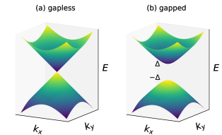
For simplicity, we assume that the energy bands of gapless and gapped Dirac materials are symmetric with respect to . The 2D Dirac material with a band gap can be described by energy dispersion,
| (1) |
where is the Planck constant, is the Fermi velocity, and is the 2D wave vector with magnitude . This energy dispersion is illustrated in Figs. 1(a) and (b) for gapless () and gapped (finite ) 2D Dirac materials, respectively.
We use the Boltzmann transport theory in the linear response regime and apply the relaxation time approximation (RTA) for an isotropic system, which is valid for our simplified model of 2D Dirac materials whose transport properties do not depend on a particular orientation in the 2D plane. Within this approach, thermoelectric properties of a 2D Dirac material can be calculated from the transport coefficients
| (2) |
where is the chemical potential (or Fermi energy), is the Fermi-Dirac distribution, and is the transport distribution function (TDF). In Eq. (2), takes a value of , , or depending on the thermoelectric properties to be calculated.
The explicit form of TDF is
| (3) |
where is the longitudinal velocity in a particular direction, is the relaxation time, and is the density of states (DOS). For isotropic systems, can be related with group velocity and dimension according to the relation , where . Therefore, we can express for the 2D Dirac materials () as:
| (4) |
For the energy-dependent relaxation time, we assume that short-range impurity scattering dominates the relaxation mechanism and as result the relaxation time is inversely proportional to the DOS Hung et al. (2017, 2018), i.e.,
| (5) |
where is the scattering coefficient (in units of ) that depends on the material dimension and confinement length Hung et al. (2018). This assumption can be derived from Fermi’s golden rule and is suitable for the scattering mechanism involving electron-phonon interactions where either acoustic or optical phonons scattered by electrons within temperature range – K Hung et al. (2018, 2017); Zhou et al. (2011b). For the sake of completeness, in Appendix A we also present the calculation result within a constant (relaxation time independent of ) git , which plays a complementary role to . Note that, under the assumption of energy-dependent relaxation time [Eq. (5)], the DOS will disappear from the TDF of Eq. (3). However, under the constant relaxation time approximation (CRTA) the DOS term will remain and is given in Eq. (37).
Using the transport coefficients, one can calculate the electrical conductivity , Seebeck coefficient , and electron thermal conductivity . They are respectively given by
| (6) | ||||
| (7) |
and
| (8) |
From these thermoelectric properties, along with the lattice thermal conductivity , we can calculate the thermoelectric figure of merit,
| (9) |
Whenever necessary, especially to simplify some equations, we will use reduced (dimensionless) variables for the energy dispersion , and also for the chemical potential, .
The transport coefficients are generally calculated by considering all bands available within . However, in most of materials, thermoelectric properties are dominated by the states near the Fermi energy. In this work, we adopt the two-band model involving a valence band and a conduction band as a minimum requirement to include the bipolar effect (or sign inversion of the Seebeck coefficient), which is always observed in materials having two different types of carriers, i.e., electrons and holes in the conduction and valence bands, respectively. A justification for the two-band model is given in Appendix B by comparing it with the multiband, first-principles calculation. In the two-band model, , , and can be written as follows Goldsmid (2010):
| (10) | ||||
| (11) | ||||
| (12) |
where the additional subscript () labels the conduction (valence) band.
III Thermoelectrics of 2D Dirac materials
The transport distribution function of 2D Dirac materials is given by
| (15) |
with the energy intervals and to be considered in the calculation of the TE integrals Eqs. (13) and (14). We also define the dimensionless gap, . The TE integral for the conduction band is then expressed as
| (16) |
with
| (17) | ||||
| (18) |
Similarly, the TE integral for the valence band is
| (19) |
with
| (20) | ||||
| (21) |
The integrals Eqs. (17) and (20) can be obtained analytically. They are:
| (22) | ||||
| (23) | ||||
| (24) | ||||
| (25) | ||||
| (26) | ||||
| (27) |
where is the polylogarithmic function. Note that and are connected via electron-hole symmetry of the system:
| (28a) | ||||
| (28b) | ||||
| (28c) | ||||
Unlike , the integrals for the conduction and valence band contributions cannot be calculated analytically, thus we employ numerical integrations to obtain git .
III.1 Gapless case
Let us firstly discuss the gapless case. In the gapless limit, so that is also equal to zero. As a result, electronic contributions from the conduction band of gapless Dirac materials to the TE quantities are solely a function of :
| (29) | ||||
| (30) | ||||
| (31) |
where is the elementary charge. For convenience, hereafter we will use the units ( V/K), , and . Note that depends on the confinement length or thickness of 2D materials Hung et al. (2018). Therefore, the natural units of electrical conductivity and thermal conductivity, i.e., and , are thickness-dependent.
The contribution of the valence band to the thermoelectric quantities , , and , can be expressed similarly with that of the conduction band:
| (32) | ||||
| (33) | ||||
| (34) |
We set the lattice thermal conductivity as an adjustable quantity,
| (35) |
where is a material parameter and may be engineered to maximize the . We assume that and dependences of are fully adjusted to the free parameter .
Based on the formulas of the two-band model [Eqs. (10)–(12)] and the electron-hole symmetry in the TE integrals [Eq. (28)], it is obvious that the Seebeck coefficient becomes zero [see Fig. 2(a)], whereas the electrical conductivity and electron thermal conductivity have constant values for whole [see Figs. 2(b) and (c)]. As a result, for the gapless 2D Dirac material considered in this approximation, we have .
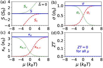
The dotted and dashed lines in Figs. 2(a)–(c) display the sole contributions of valence and conduction bands to , , and , respectively. The dramatic cancelation of the total Seebeck coefficient arising from the electron-hole symmetry in Eqs. (28). Since the relaxation time is assumed to be inversely proportional to DOS in Eq. (5), the TDF becomes energy-independent and the Seebeck coefficient completely vanishes for all doping levels. We note that the energy-dependent [Eq. (5)] fails to describe the region near the Dirac point () as the DOS vanishes. In the realistic situation should be finite even at so that the accidental, perfect cancellation should not appear.
We clarify that the CRTA, which is presented in Appendix A, gives nonzero and finite value of for the gapless 2D Dirac material, consistent with an earlier work by Sharapov and Varlamov Sharapov and Varlamov (2012). It is expected that constant relaxation time and energy-dependent relaxation time play a complementary role giving the total lifetime . Nevertheless, with the sole use of , we expose the demerit of electron-hole cancellation to the TE properties. To get rid of the poor TE performance due to the electron-hole cancellation, we may apply a magnetic field as a facilitator to break the electron-hole symmetry and thus obtain a larger, nonsaturating Seebeck coefficient Skinner and Fu (2018). However, applying the magnetic field on the order of several teslas is beyond the current practical capability of the TE industry. A simpler way to lift this electron-hole cancellation effect is by using gapped 2D Dirac materials.
III.2 Gapped case
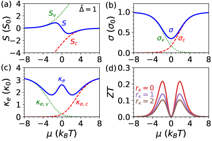
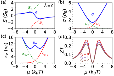
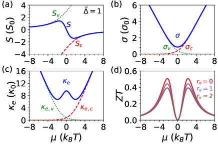
Figure 3 depicts the TE properties of the 2D gapped Dirac material for . The calculation result of Seebeck coefficient shows finite values whose sign changes across the charge neutrality point, indicating competing contribution of electron and hole, as represented by dotted and dashed lines in Fig. 3(a). Nevertheless, the perfect cancelation has now been avoided, thanks to the gap opening. The electrical conductivity exhibits a dip in the band gap and saturates to a finite value far away from the gap [Fig. 3(b)]. The electron thermal conductivity has a local maximum in the small gap limit due to the combination of of and that add each other. The resulting peaks appear slightly above the band edges with a maximum value of about for if no phonon contributes to the thermal conductivity (). The peaks monotonically decrease as the phonon contribution to the thermal conductivity increases.
IV Optimal band gap for better thermoelectrics
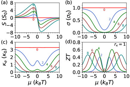
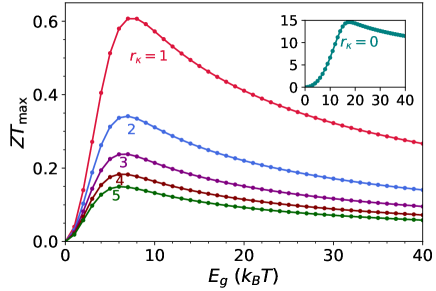
Understanding how band gap alters the TE properties is of importance for designers of TE materials. To see the evolution of TE properties with respect to the band gap, we show in Fig. 4 the calculation results of , , , and for –. As the band gap increases, the Seebeck coefficient monotonically increases while electrical and electron thermal conductivities decrease. Combined action of these interrelated quantities shall give that can be maximized by tuning . For , the value reaches maximum near the band edge and becomes largest at or corresponding band gap [Fig. 4(d)].
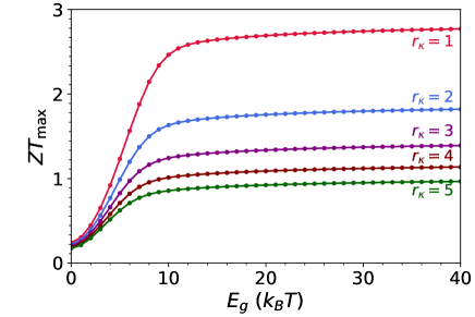
To find the optimal band gap for the 2D Dirac materials, we can numerically calculate the maximum value scanned through various doping levels and then plot (the maximum found after scanning ) as a function of and . The result is shown in Fig. 5. We can see that typically peaks at – depending on phonon thermal conductivity coefficient . By the increase of , we find that tends to be achieved at smaller band gap, saturated at . Decreasing phonon thermal conductivity through different methods such as defect engineering, heterostructures and strain is favorable to enhance . For example, the ultralow thermal conductivity denoted by will give the largest possible far above unity and it favors larger band gap of about as shown in the inset of Fig. 5.
It should be noted that the profile as a function of is sensitive to function and is also affected by the band structure. The profile for a given in the case of 2D Dirac materials has a peak when assuming due to the deterioration of bipolar effect, which means that the valence and conduction bands do not mix in the TE transport. A power law decay with the exponential factor of for at large band gaps is a hallmark of approximation for 2D gapped Dirac materials. This feature follows from asymptotic behavior of in Eq. (18) when the chemical potential reach the band edge (). In Appendixes A and C, we show different profiles for 2D Dirac and parabolic-band materials within the CRTA that do not show clear peaks of . However, we find that the optical chemical potential related to the is always very close to the band edge when and then the starting gaps to enhance appear around , which is still within –. Further works are desired to check whether the optimal gaps will appear beyond the range we find in the present study.
V Conclusions and Perspective
We have shown that optimal band gaps within – are useful for maximizing in the 2D Dirac materials, where the TE properties were calculated considering the energy-dependent relaxation time inversely proportional to the DOS. This conclusion is supplemented by considering the constant relaxation time approximation in Appendixes, as well as comparison with the parabolic-band materials. Our calculations indicate that the gapless 2D Dirac material is not good for thermoelectrics, but opening a gap of few is beneficial to enhance its TE properties.
The candidates of the gapped 2D Dirac materials that are suitable for TE applications may already possible to fabricate, such as bilayer graphene (with electrically tunable gap) and commensurate graphene-hBN heterostructure Hunt et al. (2013); Duan et al. (2016) whose minigap about tens of meV emerges due to inversion symmetry breaking. In particular, the graphene-hBN heterostructure has excellent Duan et al. (2016).
Our model is also readily extensible for other systems by using appropriate parameters, so that it may trigger further theoretical works on thermoelectrics. Multiband effect which is not considered in this calculation might enhance and can be incorporated in a straight-forward fashion within linearized Boltzmann transport equation.
Acknowledgements.
E.H. acknowledges research grant from Indonesia Toray Science Foundation. L.P.A., and B.E.G. acknowledge the financial support from Ministry of Research, Technology, and Higher Education of the Republic of Indonesia (Kemenristekdikti) through PDUPT 2018–2019. N.T.H. acknowledge the financial support from the Frontier Research Institute for Interdisciplinary Sciences, Tohoku University. N.T.H. and A.R.T.N are grateful to Prof. R. Saito (Tohoku University) for the fruitful discussion on thermoelectrics in several recent years.Appendix A Results within constant relaxation time approximation (CRTA)
Here we present the calculation of TE properties of 2D Dirac materials within the constant relaxation time approximation (CRTA). The results within this approximation overestimate the value of and in comparison to those given in the main text. As a result, the gapless 2D Dirac material will have finite (nonzero) , unlike what we have shown in the main text.
In the CRTA, the transport distribution function for the 2D Dirac materials is given by
| (36) |
where is the relaxation time constant. The density of states is defined by
| (37) |
where is degeneracies, is the confinement length, and is the Heaviside step function, i.e., if and otherwise.
After some algebra git , we can obtain the TE integral for the conduction band of the 2D Dirac material within the CRTA as
| (38) |
Similarly, the TE integral for the valence band is
| (39) |
The remaining calculation procedure to obtain the TE properties is the same as in the main text. Due to the complexity of and , the integration is performed numerically. Note that, in addition to , , and , we also need according to the recursive relation of in Eqs. (A) and (A). We obtain
| (40) |
and
| (41) |
Figures 6 and 7 show the results of TE properties of the 2D Dirac materials within the CRTA by using the same parameters as in Figs. 2 (gapless, ) and 3 (gapped, ). Within the CRTA, we can see that all the TE properties are overestimated. The most notable feature is the nonzero for the gapless 2D Dirac material [Fig. 6(a)], which leads to the finite [Fig. 6(d)] for different values. Similarly, for the gapped 2D Dirac material within the CRTA is also larger than that shown in the main text. The profile as a function of band gap for this approximation is shown in Fig. 8. There is no clear peak of , but the starting gaps to enhance are still in the range of –.
Appendix B Comparison with first-principles calculation
The two-band model developed in this work does not only grasp the essence of electronic contribution to the TE properties of 2D Dirac materials, but also reasonably fits with calculation results obtained from the density functional theory (DFT) packages. We perform band structure calculation of a relaxed structure using Perdew-Burke-Ernzerhof exchange-correlation functionals Perdew et al. (1996), as implemented in Quantum ESPRESSO, one of the most popular DFT packages Giannozzi et al. (2017). To achieve the convergence of total energy calculation, a kinetic-energy cutoff of at least eV is set for the plane-wave basis set. The periodic boundary conditions are employed and a sufficiently large vacuum layer of in the z-direction is adopted so as to avoid interaction between the adjacent layer. We obtain the lattice constant and the band gap eV without spin-orbit coupling. The TE properties are then calculated by using the BoltzTraP code Madsen and Singh (2006), which is relevant for comparison with the two-band model within CRTA because the BoltzTrap code also utilizes a constant value of relaxation time.
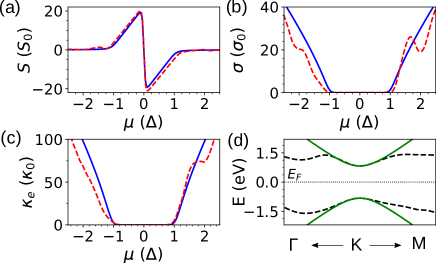
In Figs. 9(a)–(c) we show TE properties of obtained from DFT and from the two-band model within CRTA at K. Although the energy dispersion of gapped 2D Dirac materials fits only in small region near the K point [Fig. 9(d)], the Seebeck coefficient, electrical conductivity, and electronic thermal conductivity from our model fit reasonably well with those from DFT/BoltzTraP code. These results indicate that the TE properties, especially the Seebeck coeficient, of gapped 2D Dirac materials depend primarily on the size of the gap. The relatively small discrepancies between our model and the results of DFT/BoltzTraP can be attributed simply to the multiband effect and nonlinear energy dispersion far from the K point.
Appendix C Comparison with parabolic bands
The curvature of Dirac band is coupled with the size of the gap. In order to unravel this combined factors to thermoelectricity, we compare TE of the Dirac bands with that of parabolic bands. The energy dispersion of parabolic bands takes a form of , where is the effective mass, which accounts the curvature that are decoupled from the gap . The 2D parabolic bands have a constant DOS. As a result, the CRTA and approximation are equivalent.
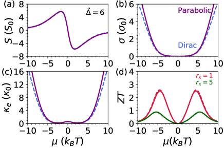
The TE integral for parabolic bands are:
| (42) | ||||
| (43) |
The remaining procedure to calculate the TE properties is the same as in the main text. We again perform numerical calculation for all the integrals above. Figures 10(a)-(d) show comparison of TE quantities for the 2D parabolic-band (solid lines) and Dirac materials (dashed lines) within the CRTA. The TE quantities are nearly unchanged for different shape of bands. These results are obvious because the contribution of relaxation from each energy state is assumed to be constant in the CRTA.
We then plot vs energy gap () by scanning through chemical potential . The result is shown in Fig. 11(a). monotonically increases as increases up to and saturates at above . This saturation is expected because we assume no gap dependent relaxation time (mobility). Figure 11(b) shows the optimal chemical potential that gives maximum ZT. It is apparent that is located very close to the band edge, indicated by as the dashed line. The flat profile of vs can be understood from Eq. (42) that becomes a constant when . We note that when is at the edge of conduction or valence band, all systems are doped with the same charge concentration irrespective of the band gap entering the regime of degenerate semiconductors. As a result, is flat at large band gap. These results are qualitatively similar to the Dirac band with CRTA (see Fig. 8) and to 3D semiconductors Sofo and Mahan (1994).
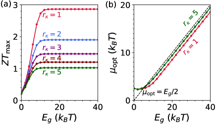
We, therefore, define the optimal bandgap at the turning point before saturates, because increasing the band gap would require larger , which is harder to achieve. For the 2D parabolic-band materials, the optimal band gaps with such a definition are located around 10 . Furthermore, we should note that independent of band gap is unrealistic because highly doped semiconductors are generally suffers large impurity scattering resulting in the decrease of mobility and Yu et al. (2017). We conclude that the thermoelectric properties are relatively insensitive to the detailed shape of band structures as long as the CRTA is concerned. The change of approximation will affect the vs profile for non-parabolic bands (such as the Dirac band) but it does not change the optimal band gap substantially.
References
- Goldsmid (2010) H. J. Goldsmid, Introduction to Thermoelectricity (Springer-Verlag, Berlin Heidelberg, 2010).
- Heremans et al. (2013) J. P. Heremans, M. S. Dresselhaus, L. E. Bell, and D. T. Morelli, “When thermoelectrics reached the nanoscale,” Nat. Nanotechnol. 8, 471–473 (2013).
- Pei et al. (2011) Y. Pei, X. Shi, A. LaLonde, H. Wang, L. Chen, and G. J. Snyder, “Convergence of electronic bands for high performance bulk thermoelectrics,” Nature 473, 66–69 (2011).
- Biswas et al. (2012) K. Biswas, J. He, I. D. Blum, C. I. Wu, T. P. Hogan, D. N. Seidman, V. P. Dravid, and M. G. Kanatzidis, “High-performance bulk thermoelectrics with all-scale hierarchical architectures,” Nature 489, 414 (2012).
- Hicks and Dresselhaus (1993a) L. D. Hicks and M. S. Dresselhaus, “Effect of quantum-well structures on the thermoelectric figure of merit,” Phys. Rev. B 47, 12727 (1993a).
- Hung et al. (2016) N. T. Hung, E. H. Hasdeo, A. R. T. Nugraha, M. S. Dresselhaus, and R. Saito, “Quantum effects in the thermoelectric power factor of low-dimensional semiconductors,” Phys. Rev. Lett. 117, 036602 (2016).
- Majumdar (2004) A. Majumdar, “Thermoelectricity in semiconductor nanostructures,” Science 303, 777 (2004).
- Vining (2009) C. B. Vining, “An inconvenient truth about thermoelectrics,” Nat. Mater. 8, 83 (2009).
- Mahan and Sofo (1996) G. D. Mahan and J. O. Sofo, “The best thermoelectric,” Proc. Natl. Acad. Sci. U.S.A. 93, 7436 (1996).
- Zhou et al. (2011a) J. Zhou, R. Yang, G. Chen, and M. S. Dresselhaus, “Optimal bandwidth for high efficiency thermoelectrics,” Phys. Rev. Lett. 107, 226601 (2011a).
- Sofo and Mahan (1994) J. O. Sofo and G. D. Mahan, “Optimum band gap of a thermoelectric material,” Phys. Rev. B 49, 4565 (1994).
- Hicks and Dresselhaus (1993b) L. D. Hicks and M. S. Dresselhaus, “Thermoelectric figure of merit of a one-dimensional conductor,” Phys. Rev. B 47, 16631 (1993b).
- Hicks et al. (1996) L. D. Hicks, T. C. Harman, X. Sun, and M. S. Dresselhaus, “Experimental study of the effect of quantum-well structures on the thermoelectric figure of merit,” Phys. Rev. B 53, R10493 (1996).
- Dresselhaus et al. (2007) M. S. Dresselhaus, G. Chen, M. Y. Tang, R. G. Yang, H. Lee, D. Z. Wang, Z. F. Ren, J. P. Fleurial, and P. Gogna, “New directions for low-dimensional thermoelectric materials,” Adv. Mater. 19, 1043 (2007).
- Zhang and Zhang (2017) G. Zhang and Y.-W. Zhang, “Thermoelectric properties of two-dimensional transition metal dichalcogenides,” J. Mater. Chem. C 5, 7684 (2017).
- Castellanos-Gomez (2016) A. Castellanos-Gomez, “Why all the fuss about 2D semiconductors?” Nat. Photonics 10, 202 (2016).
- Hippalgaonkar et al. (2017) K. Hippalgaonkar, Y. Wang, Y. Ye, D. Y. Qiu, H. Zhu, Y. Wang, J. Moore, S. G. Louie, and X. Zhang, “High thermoelectric power factor in two-dimensional crystals of MoS2,” Phys. Rev. B 95, 115407 (2017).
- Yang et al. (2014) K. Yang, S. Cahangirov, A. Cantarero, A. Rubio, and R. D’Agosta, “Thermoelectric properties of atomically thin silicene and germanene nanostructures,” Phys. Rev. B 89, 125403 (2014).
- Duan et al. (2016) J. Duan, X. Wang, X. Lai, G. Li, K. Watanabe, T. Taniguchi, M. Zebarjadi, and E. Y. Andrei, “High thermoelectricpower factor in graphene/hBN devices,” Proc. Natl. Acad. Sci. USA 113, 14272 (2016).
- Ni et al. (2012) Z. Ni, Q. Liu, K. Tang, J. Zheng, J. Zhou, R. Qin, Z. Gao, D. Yu, and J. Lu, “Tunable bandgap in silicene and germanene,” Nano Lett. 12, 113 (2012).
- Zaminpayma and Nayebi (2016) E. Zaminpayma and P. Nayebi, “Band gap engineering in silicene: A theoretical study of density functional tight-binding theory,” Phys. E 84, 555 (2016).
- Lee et al. (2016) M. J. Lee, J. H. Ahn, J. H. Sung, H. Heo, S. G. Jeon, W. Lee, J. Y. Song, K.-H. Hong, B. Choi, S. H. Lee, and M. H. Jo, “Thermoelectric materials by using two-dimensional materials with negative correlation between electrical and thermal conductivity,” Nat. Commun. 7, 12011 (2016).
- Wickramaratne et al. (2015) D. Wickramaratne, F. Zahid, and R. K. Lake, “Electronic and thermoelectric properties of van der Waals materials with ring-shaped valence bands,” J. Appl. Phys. 118, 075101 (2015).
- Ghaemi et al. (2010) P. Ghaemi, R. S. K. Mong, and J. E. Moore, “In-plane transport and enhanced thermoelectric performance in thin films of the topological insulators Bi2Te3 and Bi2Se3,” Phys. Rev. Lett. 105, 166603 (2010).
- Maassen and Lundstrom (2013) J. Maassen and M. Lundstrom, “A computational study of the thermoelectric performance of ultrathin Bi2Te3 films,” Appl. Phys. Lett. 102, 093103 (2013).
- Zhao et al. (2014) L. D. Zhao, S. H. Lo, Y. Zhang, H. Sun, G. Tan, C. Uher, C. Wolverton, V. P. Dravid, and M. G. Kanatzidis, “Ultralow thermal conductivity and high thermoelectric figure of merit in SnSe crystals,” Nature 508, 374 (2014).
- Gibbs et al. (2015) Z. M. Gibbs, H. S. Kim, H. Wang, and G. J. Snyder, “Band gap estimation from temperature dependent seebeck measurement-deviations from the relation,” Appl. Phys. Lett. 106, 022112 (2015).
- Anno et al. (2017) Y. Anno, Y. Imakita, K. Takei, S. Akita, and T. Arie, “Enhancement of graphene thermoelectric performance through defect engineering,” 2D Mat. 4, 025019 (2017).
- Qin et al. (2017) D. Qin, X. J. Ge, G. Q. Ding, G. Y. Gao, and J. T. Lu, “Strain-induced thermoelectric performance enhancement of monolayer ZrSe2,” RSC Adv. 7, 47243 (2017).
- Kim et al. (2015) S. I. Kim, K. H. Lee, H. A. Mun, H. S. Kim, S. W. Hwang, J. W. Roh, D. J. Yang, W. H. Shin, X. S. Li, Y. H. Lee, G. J. Snyder, and S. W. Kim, “Dense dislocation arrays embedded in grain boundaries for high-performance bulk thermoelectrics,” Science 348, 109–114 (2015).
- Hung et al. (2017) N. T. Hung, A. R. T. Nugraha, and R. Saito, “Two-dimensional InSe as a potential thermoelectric material,” Appl. Phys. Lett. 111, 092107 (2017).
- Hung et al. (2018) N. T. Hung, A. R. T. Nugraha, and R. Saito, “Universal curve of optimum thermoelectric figures of merit for bulk and low-dimensional semiconductors,” Phys. Rev. Appl. 9, 024019 (2018).
- Zhou et al. (2011b) J. Zhou, R. Yang, G. Chen, and M. S. Dresselhaus, “Optimal bandwidth for high efficiency thermoelectrics,” Phys. Rev. Lett. 107, 226601 (2011b).
- (34) Detailed notes, derivations, and codes for all results in this paper (both in the main text and Appendix) are available at http://github.com/artnugraha/DiracTE.
- Sharapov and Varlamov (2012) S. G. Sharapov and A. A. Varlamov, “Anomalous growth of thermoelectric power in gapped graphene,” Phys. Rev. B 86, 035430 (2012).
- Skinner and Fu (2018) B. Skinner and L. Fu, “Large, nonsaturating thermopower in a quantizing magnetic field,” Sci. Adv. 4, eaat2621 (2018).
- Hunt et al. (2013) B. Hunt, J. D. Sanchez-Yamagishi, A. F. Young, M. Yankowitz, B. J. LeRoy, K. Watanabe, T. Taniguchi, P. Moon, M. Koshino, P. Jarillo-Herrero, and R. C. Ashoori, “Massive Dirac fermions and Hofstadter butterfly in a van der Waals heterostructure,” Science 340, 1427 (2013).
- Perdew et al. (1996) J. P. Perdew, K. Burke, and M. Ernzerhof, “Generalized gradient approximation made simple,” Phys. Rev. Lett. 77, 3865–3868 (1996).
- Giannozzi et al. (2017) P. Giannozzi, O. Andreussi, T. Brumme, O. Bunau, M. Buongiorno Nardelli, M. Calandra, R. Car, C. Cavazzoni, D. Ceresoli, M. Cococcioni, N. Colonna, I. Carnimeo, A. Dal Corso, S. de Gironcoli, P. Delugas, R. A. DiStasio, A. Ferretti, A. Floris, G. Fratesi, G. Fugallo, R. Gebauer, U. Gerstmann, F. Giustino, T. Gorni, J. Jia, M. Kawamura, H.-Y. Ko, A. Kokalj, E. Küçükbenli, M. Lazzeri, M. Marsili, N. Marzari, F. Mauri, N. L. Nguyen, H.-V. Nguyen, A. Otero-de-la-Roza, L. Paulatto, S. Poncé, D. Rocca, R. Sabatini, B. Santra, M. Schlipf, A. P. Seitsonen, A. Smogunov, I. Timrov, T. Thonhauser, P. Umari, N. Vast, X. Wu, and S. Baroni, “Advanced capabilities for materials modelling with Quantum ESPRESSO,” J. Phys. Condens. Matter 29, 465901 (2017).
- Madsen and Singh (2006) G. K. H. Madsen and D. J. Singh, “BoltzTraP. A code for calculating band-structure dependent quantities,” Comput. Phys. Commun. 175, 67–71 (2006).
- Yu et al. (2017) Z. Yu, Z.-Y. Ong, S. Li, J.-B. Xu, G. Zhang, Shi Y. Zhang, Y.-W., and X. Wang, “Analyzing the carrier mobility in transition-metal dichalcogenide MoS2 field-effect transistors,” Adv. Funct. Mater. 27, 1604093 (2017).