A Framework for Evaluating Security in the Presence of Signal Injection Attacks
Abstract
Sensors are embedded in security-critical applications from medical devices to nuclear power plants, but their outputs can be spoofed through electromagnetic and other types of signals transmitted by attackers at a distance. To address the lack of a unifying framework for evaluating the effects of such transmissions, we introduce a system and threat model for signal injection attacks. We further define the concepts of existential, selective, and universal security, which address attacker goals from mere disruptions of the sensor readings to precise waveform injections. Moreover, we introduce an algorithm which allows circuit designers to concretely calculate the security level of real systems. Finally, we apply our definitions and algorithm in practice using measurements of injections against a smartphone microphone, and analyze the demodulation characteristics of commercial Analog-to-Digital Converters (ADCs). Overall, our work highlights the importance of evaluating the susceptibility of systems against signal injection attacks, and introduces both the terminology and the methodology to do so.111 This article is the extended technical report version of the paper presented at ESORICS 2019. DOI: 10.1007/978-3-030-29959-0_25.
Keywords:
Signal Injection Attacks Security Metrics Analog-to-Digital Converters Electromagnetic Interference Non-linearities1 Introduction
In our daily routine we interact with dozens of sensors: from motion detection in home security systems and tire pressure monitors in cars, to accelerometers in smartphones and heart rate monitors in smartwatches. The integrity of these sensor outputs is crucial, as many security-critical decisions are taken in response to the sensor values. However, specially-crafted adversarial signals can be used to remotely induce waveforms into the outputs of sensors, thereby attacking pacemakers [10], temperature sensors [5], smartphone microphones [9], and car-braking mechanisms [20]. These attacks cause a system to report values which do not match the true sensor measurements, and trick it into performing dangerous actions such as raising false alarms, or even delivering defibrillation shocks.
The root cause of these vulnerabilities lies in the unintentional side-effects of the physical components of a system. For example, the wires connecting sensors to microcontrollers behave like low-power, low-gain antennas, and can thus pick up high-frequency electromagnetic radiations. Although these radiations are considered “noise” from an electrical point of view, hardware imperfections in the subsequent parts of the circuit can transform attacker injections into meaningful waveforms. Specifically, these radiations are digitized along with the true sensor outputs, which represent a physical property as an analog electrical quantity. This digitization process is conducted by Analog-to-Digital Converters (ADCs), which, when used outside of their intended range, can cause high-frequency signals to be interpreted as meaningful low-frequency signals.
Despite the potential that signal injection attacks have to break security guarantees, there is no unifying framework for evaluating the effect of such adversarial transmissions. Our work fills this gap through the following contributions:
-
1.
We propose a system model which abstracts away from engineering concerns associated with remote transmissions, such as antenna design (Section 2).
-
2.
We define security against adversarial signal injection attacks. Our definitions address effects ranging from mere disruptions of the sensor readings, to precise waveform injections of attacker-chosen values (Section 3).
-
3.
We introduce an algorithm to calculate the security level of a system under our definitions and demonstrate it in practice by injecting “OK Google” commands into a smartphone (Section 4).
-
4.
We investigate how vulnerable commercial ADCs are to malicious signal injection attacks by testing their demodulation properties (Section 5).
-
5.
We discuss how our model can be used to inform circuit design choices, and how to interpret defense mechanisms and other types of signal injection attacks in its context (Section 6).
Overall, our work highlights the importance of testing systems against signal injection attacks, and proposes a methodology to test the security of real devices.
2 System and Adversary Model
Remote signal injection attacks pose new challenges from a threat-modeling perspective, since the electrical properties of systems suggest that adversaries cannot arbitrarily and precisely change any sensor reading. To create a threat model and define security in its context, we need to first abstract away from specific circuit designs and engineering concerns related to remote transmissions. To do so, we separate the behavior of a system into two different transfer functions. The first function describes circuit-specific behavior, including how adversarial signals enter the circuit (e.g., through PCB wires acting as antennas), while the second one is ADC-specific, and dictates how the signals which have made it into the circuit are digitized. We describe this model in greater detail in Section 2.1, taking a necessary detour into electrical engineering to show why our proposal makes for a good system model. We then explain some sources of measurement errors even in the absence of an adversary in Section 2.2 and finish by detailing the capabilities and limitations of the adversary in Section 2.3. Both sub-sections are crucial in motivating the security definitions of Section 3.
2.1 Circuit Model
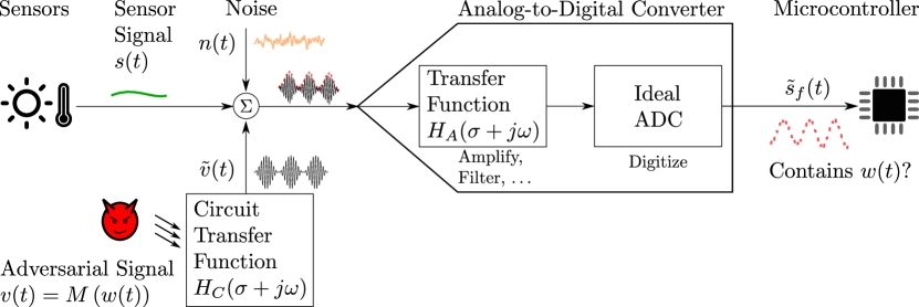
Analog-to-Digital Converters (ADCs) are central in the digitization process of converting signals from the analog to the digital realm, and our circuit block diagram (Figure 1) reflects that. In the absence of an adversary, the ADC digitizes the sensor signal as well as the environmental noise , and transfers the digital bits to a microcontroller. We model the ADC in two parts: an “ideal” ADC which simply digitizes the signal, and a transfer function . This transfer function describes the internal behavior of the ADC, which includes effects such as filtering and amplification. The digitized version of the signal depends both on this transfer function, and the sampling frequency of the ADC. An adversarial signal can enter the system (e.g., through the wires connecting the sensor to the ADC) and add to the sensor signal and the noise. This process can be described by a second, circuit-specific transfer function , which transforms the adversarial signal into . Note that components such as external filters and amplifiers in the signal path between the point of injection and the ADC can be included in either or . We include them in when they also affect the sensor signal , but in when they are specific to the coupling effect. and are discussed in detail below.
Circuit Transfer Function . To capture the response of the circuit to external signal injections, we introduce a transfer function . This transfer function explains why the adversarial waveforms must be modulated, and why it is helpful to try and reduce the number of remote experiments to perform. For electromagnetic interference (EMI) attacks, the wires connecting the sensor to the ADC pick up signals by acting as (unintentional) low-power and low-gain antennas, which are resonant at specific frequencies related to the inverse of the wire length [12]. Non-resonant frequencies are attenuated more, so for a successful attack the adversary must transmit signals at frequencies with relatively low attenuation. For short wires, these frequencies are in the range [12], so the low-frequency waveform that the adversary wants to inject into the output of the ADC may need to be modulated over a high-frequency carrier using a function . We denote this modulated version of the signal by .
is also affected by passive and active components on the path to the ADC, and can also be influenced by inductive and capacitive coupling for small transmission distances, as it closely depends on the circuit components and their placement. Specifically, it is possible for 2 circuits with “the same components, circuit topology and placement area” to have different EMI behavior depending on the component placement on the board [13]. Despite the fact that it is hard to mathematically model and predict the behavior of circuits in response to different signal transmissions, can still be determined empirically using frequency sweeps. It presents a useful abstraction, allowing us to separate the behavior of the ADC (which need only be determined once, for instance by the manufacturer) from circuit layout and transmission details.
Note, finally, that can also account for distance factors between the adversary and the circuit under test: due to the Friis transmission formula [4], as distance doubles, EMI transmission power needs to quadruple. This effect can be captured by increasing the attenuation of by , while defense mechanisms such as shielding can be addressed similarly. This approach allows us to side-step engineering issues of remote transmissions and reduce the number of parameters used in the security definitions we propose in Section 3.

ADC Transfer Function . Every system with sensors contains one or more ADCs, which may even be integrated into the sensor chip itself. ADCs are not perfect, but contain components which may cause a mismatch between the “true” value at the ADC input and the digitized output. In this section, we describe how these components affect the digitization process.
Although there are many types of ADCs, every ADC contains three basic components: a “sample- or track-and-hold circuit where the sampling takes place, the digital-to-analog converter and a level-comparison mechanism” [15]. The sample-and-hold component acts as a low-pass filter, and makes it harder for an adversary to inject signals modulated at high frequencies. However, the level-comparison mechanism is essentially an amplifier with non-linearities which induces DC offsets, and allows low-frequency intermodulation products to pass through. These ADC-specific transformations, modeled through , unintentionally demodulate high-frequency signals which are not attenuated by . They are explored in more detail in Section 5 and Appendix 0.A.
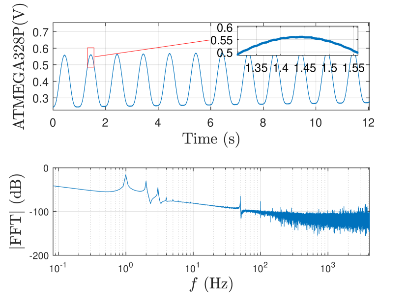
Sample-And-Hold Filter Characteristics. A sample-and-hold (S/H) mechanism is an circuit connected to the analog input, with the resistor and the capacitor connected in series (Figure 2). The transfer function of the voltage across the capacitor is , and the magnitude of the gain is . As the angular frequency increases, the gain is reduced: the S/H mechanism acts as a low-pass filter. The cutoff frequency is thus , which is often higher than the ADC sampling rate (Section 5). Hence, “aliasing” occurs when signals beyond the Nyquist frequency are digitized by the ADC: high-frequency signals become indistinguishable from low-frequency signals which the ADC can sample accurately.
Amplifier Non-Linearities. Every ADC contains amplifiers: a comparator, and possibly buffer and differential amplifiers. Many circuits also contain additional external amplifiers to make weak signals measurable. All these amplifiers have harmonic and intermodulation non-linear distortions [17], which an adversary can exploit. Harmonics are produced when an amplifier transforms an input to an output . In particular, if , then:
This equation shows that “the frequency spectrum of the output contains a spectral component at the original (fundamental) frequency, [and] at multiples of the fundamental frequency (harmonic frequencies)” [17]. Moreover, the output includes a DC component, which depends only on the even-order non-linearities of the system. Besides harmonics, intermodulation products arise when the input signal is a sum of two sinusoids (for instance when the injected signal sums with the sensor signal): . In that case, the output signal contains frequencies of the form for integers . These non-linearities demodulate attacker waveforms, even when they are modulated on high-frequency carriers.
Diode Rectification. Figure 2 shows that the input to an ADC can contain reverse-biased diodes to ground and to protect the input from Electrostatic Discharge (ESD). When the input to the ADC is negative, or when it exceeds , the diodes clamp it, causing non-linear behavior. When the sensor signal is positive, this behavior is also asymmetric, causing a DC shift [17], which compounds with the amplifier non-linearities.
Conclusion. All ADCs contain the same basic building blocks, modeled through . Although the sample-and-hold mechanism should attenuate high-frequency signals beyond the maximum sampling rate of the ADC, non-linearities due to ESD diodes and amplifiers in the ADC cause DC offsets and the demodulation of signals through harmonics and intermodulation products. Section 5 and Appendix 0.A exemplify these effects through experiments on different ADCs.
2.2 Sampling Errors in the Absence of an Adversary
The digitization process through ADCs entails errors due to quantization and environmental noise. Quantization errors exist due to the inherent loss of accuracy in the sampling process. An ADC can only represent values within a range, say between and volts, with a finite binary representation of bits, called the resolution of the ADC. In other words, every value between and is mapped to one of the values that can be represented using bits. As a result, there is a quantization error between the true sensor analog value and the digitized value . The maximum value of this error is
| (1) |
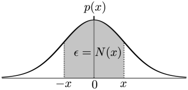
The second source of error comes from environmental noise, which may affect measurements. We assume that this noise, denoted by , is independent of the signal being measured, and that it comes from a zero-mean distribution, i.e., that the noise is white. The security definitions we introduce in Section 3 require an estimate of the level of noise in the system, so we introduce some relevant notation here. We assume that follows a probability distribution function (PDF) , and define as the probability that the noise is between and , as shown in Figure 3, i.e.,
Note that typically the noise is assumed to come from a normal distribution, but this assumption is not necessary in our models and definitions.
We are also interested in the inverse of this function, where given a probability , we want to find such that . For this , the probability that the noise magnitude falls within is , as also shown in Figure 3. Because for some distributions there might be multiple for which , we use the smallest such value:
| (2) |
Since is an increasing function, so is .
To account for repeated measurements, we introduce a short-hand for sampling errors, which we denote by . The sampling errors depend on the sensor input into the ADC , the sampling rate , the discrete output of the ADC as well as the conversion delay , representing the time the ADC takes for complete a conversion:
| (3) |
2.3 Adversary Model
Our threat model and definitions can capture a range of attacker goals, from attackers who merely want to disrupt sensor outputs, to those who wish to inject precise waveforms into a system. We define these notions precisely in Section 3, but here we describe the attacker capabilities based on our model of Figure 1. Specifically, in our model, the adversary can only alter the transmitted adversarial signal . He/she cannot directly influence the sensor signal , the (residual) noise , or the transfer functions and . The adversary knows , , and the distribution of the noise , although the true sensor signal might be hidden from the adversary (see Section 3.2). The only constraint placed on the adversarial signal is that the attacker is only allowed to transmit signals whose peak voltage level is bounded by some constant , i.e., for all . We call this adversary a -bound adversary, and all security definitions are against such bounded adversaries.
We choose to restrict voltage rather than restricting power or distance, as it makes for a more powerful adversarial model. Our model gives the adversary access to any physical equipment necessary (such as powerful amplifiers and highly-directional antennas), while reducing the number of parameters needed for our security definitions of Section 3. Distance and power effects can be compensated directly through altering , or indirectly by integrating them into , as discussed in Section 2.1.
3 Security Definitions
Using the model of Figure 1, we can define security in the presence of signal injection attacks. The -bound adversary is allowed to transmit any waveform , provided that for all : the adversary is only constrained by the voltage budget. Whether or not the adversary succeeds in injecting the target waveform into the output of the system depends on the transfer functions and . For a given system described by and , there are three outcomes against an adversary whose only restriction is voltage:
-
1.
The adversary can disturb the sensor readings, but cannot precisely control the measurement outputs, an attack we call existential injection. The lack of existential injections can be considered universal security.
-
2.
The adversary can inject a target waveform into the ADC outputs with high fidelity, performing a selective injection. If the adversary is unable to succeed, the system is selectively secure against .
-
3.
The adversary can universally inject any waveform . If there is any non-trivial waveform for which he/she fails, the system is existentially secure.
This section sets out to precisely define the above security notions by accounting for noise and quantization error (Equation (1)). Our definitions capture the intuition that systems are secure when there are no adversarial transmissions, and are “monotonic” in voltage, i.e., systems are more vulnerable against adversaries with access to higher-powered transmitters. Our definitions are also monotonic in noise: in other words, in environments with low noise, even a small disturbance of the output is sufficient to break the security of a system. Section 3.1 evaluates whether an adversary can disturb the ADC output away from its correct value sufficiently. Section 3.2 then formalizes the notion of selective security against target waveforms . Finally, Section 3.3 introduces universal injections by defining what a non-trivial waveform is. The three types of signal injection attacks, the corresponding security properties, and the ensuing ADC errors (injected waveforms) are summarized in Table 1.222 The terminology chosen was inspired by attacks against signature schemes, where how broken a system is depends on what types of messages an attacker can forge [8].
| Security | Injection | ADC Error |
|---|---|---|
| Universal | Existential | Bounded away from |
| Selective | Selective | Target waveform |
| Existential | Universal | Non-trivial waveforms |
3.1 Existential Injection, Universal Security
The most primitive type of signal injection attack is a simple disruption of the sensor readings. There are two axes in which this notion can be evaluated: adversarial voltage and probability of success (success is probabilistic, as noise is a random variable). For a fixed probability of success, we want to determine the smallest voltage level for which an attack is successful. For a fixed voltage level, we want to find the probability of a successful attack. Alternatively, if we fix both the voltage and the probability of success, we want to determine if a system is secure against disruptive signal injection attacks.
The definition for universal security is a formalization of the above intuition, calling a system secure when, even in the presence of injections (bounded by adversarial voltage), the true analog sensor value and the ADC digital output do not deviate by more than the quantization error and the noise, with sufficiently high probability. Mathematically:
Definition 1 (Universal Security, Existential Injection)
For , and , we call a system universally -secure if
| (4) |
for every adversarial waveform , with for all . is the quantization error of the system, is the noise distribution inverse defined in Equation (2), and is the sampling error as defined by Equation (3). The probability is taken over the duration of the attack, i.e., at each sampling point within the interval . We call a successful attack an existential injection, and simply call a system universally -secure, when is implied.
We first show that in the absence of injections, the system is universally -secure for all . Indeed, let , so that . Then, in the absence of injections,
which holds for all , as desired. This proof is precisely the reason for requiring a noise level and probability of at least 50% in the definition: the proof no longer works if is replaced by just . In other words, mere noise would be classified as an attack by the modified definition.
Voltage. We now show that a higher adversarial voltage budget can only make a system more vulnerable. Indeed, if a system is universally -secure, then it is universally -secure for . For this, it suffices to prove the contrapositive, i.e., that if a system is not universally -secure, then it is not universally -secure. For the proof, let be an adversarial waveform with such that Equation (4) does not hold, which exists by the assumption that the system is not universally -secure. Then, by the transitive property, , making a valid counterexample for universal security.
Probability. The third property we show is probability monotonicity, allowing us to define a “critical threshold” for , above which a system is universally secure (for a fixed ), and below which a system is not universally secure. Indeed, for fixed , if a system is universally -secure, then it is universally -secure for , as
because is increasing. The contrapositive is, of course, also true: if a system is not universally secure for a given , it is also not universally secure for with .
Thresholds. For a given security level , then, we can talk about the maximum (if any) such that a system is universally -secure, or conversely the minimum (if any) such that a system is not universally -secure. This is the critical universal voltage level for the given . Moreover, for any , there is a unique critical universal security threshold such that the system is universally -secure for and not universally -secure for . By convention we take if the system is secure for all , and if there is no for which the system is secure. This critical threshold indicates the security level of a system: the lower is, the better a system is protected against signal injection attacks.
3.2 Selective Injection and Security
The second definition captures the notion of security against specific target waveforms : we wish to find the probability that a -bounded adversary can make appear in the output of the ADC. Conversely, to define security in this context, we must make sure that the digitized signal differs from the waveform with high probability, even if plenty of noise is allowed. There are two crucial points to notice about the waveform . First, is not the raw signal the adversary is transmitting, as this signal undergoes two transformations via and . Instead, is the signal that the adversary wants the ADC to think that it is seeing, and is usually a demodulated version of (see Figure 1). Second, does not necessarily cancel out or overpower , because that would require predictive modeling of the sensor signal . However, if the adversary can predict (e.g., by monitoring the output of the ADC, or by using identical sensors), we can then ask about security against the waveform instead. Given this intuition, we can define selective security as follows:
Definition 2 (Selective Security, Selective Injection)
For , and , a system is called selectively -secure if
| (5) |
for every adversarial waveform , with for all , where the probability is taken over the duration of the attack. is the quantization error of the system, is the noise distribution inverse defined in Equation (2), and during sampling periods, and otherwise. We call a successful attack a selective injection, and simply call a system selectively -secure, when and are clear from context.
This definition is monotonic in voltage and the probability of success, allowing us to talk about “the” probability of success for a given waveform:
Voltage. A similar argument shows that increasing can only make a secure system insecure, but not vice versa, i.e., that if a system is selectively -secure, then it is selectively -secure for . We can thus define the critical selective voltage level for a given and .
Probability. If a system is selectively -secure (against a target waveform and voltage budget), then it is selectively -secure for , because
If the system is not selectively -secure, then it is not selectively -secure.
Given the above, for a given waveform and fixed , we can define a waveform-specific critical selective security threshold such that the system is vulnerable for all with and secure for all with . By convention we take if there is no for which the system is vulnerable, and if there is no for which the system is secure.
Threshold Relationship. The critical universal threshold of a system is related to the critical selective threshold against the zero waveform through the equation . Indeed, if a system is not universally -secure, then , so , making the system selectively -secure for the zero waveform. Conversely, if a system is selectively -secure for the zero waveform, then it is not universally -secure. The fact that a low critical universal threshold results in a high critical selective threshold for the zero threshold is not surprising: it is easy for an adversary to inject a zero signal by simply not transmitting anything.
3.3 Universal Injection, Existential Security
The final notion of security is a weak one, which requires that the adversary cannot inject at least one “representable” waveform into the system, i.e., one which is within the ADC limits. We can express this more precisely as follows:
Definition 3 (Representable Waveform)
A waveform is called representable if it is within the ADC voltage levels, and has a maximum frequency component bounded by the Nyquist frequency of the ADC. Mathematically, and .
Using this, we can define security against at least one representable waveform:
Definition 4 (Existential Security, Universal Injection)
For , and , a system is called existentially -secure if there exists a representable waveform for which the system is selectively -secure. We call a system existentially -secure when is clear. If there is no such , we say that the adversary can perform any universal injection.
As above, voltage and probability are monotonic in the opposite direction.
Voltage. If a system is existentially -secure, then it is -secure for . By assumption, there is a representable such that the system is selectively -secure. By the previous section, this system is -secure, concluding the proof.
Probability. If a system is existentially -secure, then it is -secure for . By assumption, there is a representable such that the system is selectively -secure. By the previous section, the system is also -secure, as desired.
Thresholds. Extending the definitions of the previous sections, for fixed we can define a critical existential voltage level below which a system is existentially -secure, and above which the system is existentially -insecure. Similarly, for a fixed adversarial voltage we can define the critical existential security threshold , above which the system is existentially secure, and below which the system is insecure.
In some cases, security designers may wish to adjust the definitions to restrict target waveforms (and existential security counterexamples) even further. For instance, we might wish to check whether an adversary can inject all waveforms which are sufficiently bounded away from 0, periodic waveforms, or waveforms of a specific frequency. The proofs for voltage and probability monotonicity still hold, allowing us to talk about universal security against -representable waveforms: waveforms which are representable and also in a set .
4 Security Evaluation of a Smartphone Microphone
| Injection | Resulting Signal | Crit. Thres. |
|---|---|---|
| Existential | ||
| Selective | ||
| Selective | ||
| Universal | “OK Google” commands |
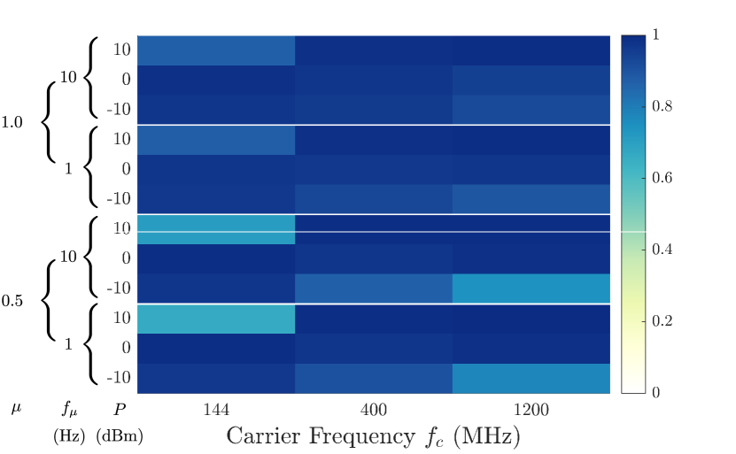
In this section, we illustrate how our security definitions can be used to determine the security level of a commercial, off-the-shelf smartphone microphone. We first introduce an algorithm to calculate the critical selective security threshold against a target waveform in Section 4.1. We then use the algorithm to calculate the critical thresholds of a smartphone in Section 4.2. Finally, we comment on universal security in Section 4.3, where we show that we are able to inject complex “OK Google” commands. We summarize our results in Table 2, while Appendix 0.A contains additional experiments for further characterization of the smartphone’s ADC.
4.1 Algorithm for Selective Security Thresholds
In this section, we introduce an algorithm to calculate the critical selective security threshold of a system against a target waveform , using a transmitted signal . The first step in the algorithm (summarized in pseudocode as Algorithm 1) is to determine the noise distribution. To that end, we collect measurements of the system output during the injection and pick one as the reference signal. We then pick of them to calculate the noise (estimation signals), while the remaining are used to verify our calculations (validation signals).
Our algorithm first removes any DC offset and re-scales the measurements so that the root-mean-square (RMS) voltages of the signals are the same. The repeated measurements are then phase-aligned, and we calculate the distance between the reference signal and the estimation signals. The average of this distance should be very close to 0, as the signals are generated in the same way. However, the standard deviation is non-zero, so we can model noise as following a zero-mean normal distribution . We can then find the critical threshold between the reference signal and any target ideal waveform as follows: we first detrend, scale, and align the ideal signal to the reference waveform, as with the estimation signals. Then, we calculate the errors (distance) between the ideal and the reference signal. Finally, we perform a binary search for different values of , in order to find the largest for which Equation (5) does not hold: this is the critical threshold . To calculate the inverse of the noise, we use the percentile point function , which is the inverse of the cumulative distribution function, and satisfies . Note that since the critical universal threshold is related to the selective critical threshold of the zero waveform through (Section 3.2), the same algorithm can be used to calculate the critical universal security threshold .
4.2 Existential and Selective Injections into a Smartphone
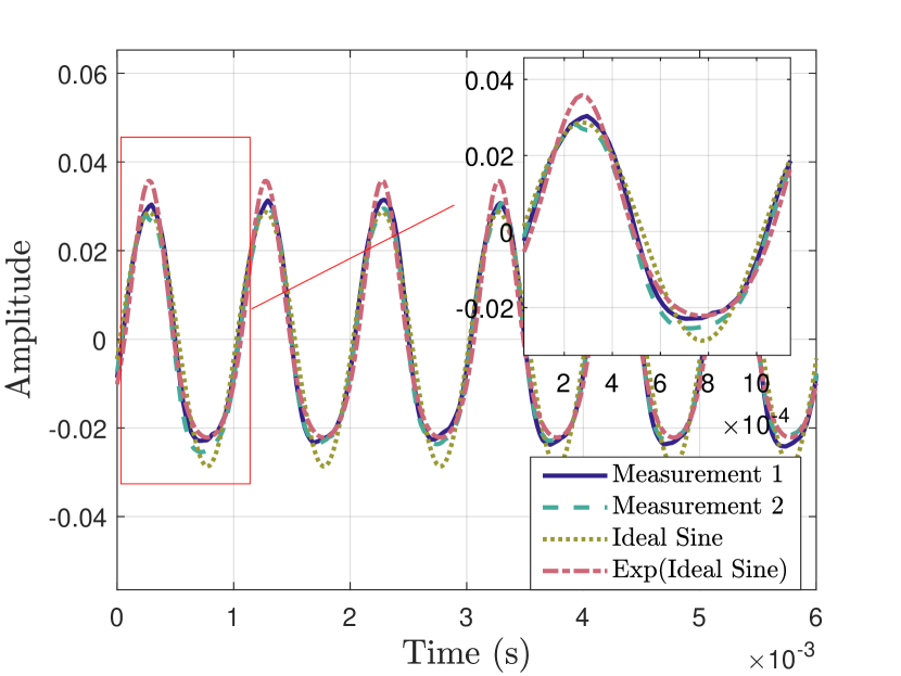
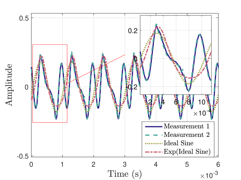
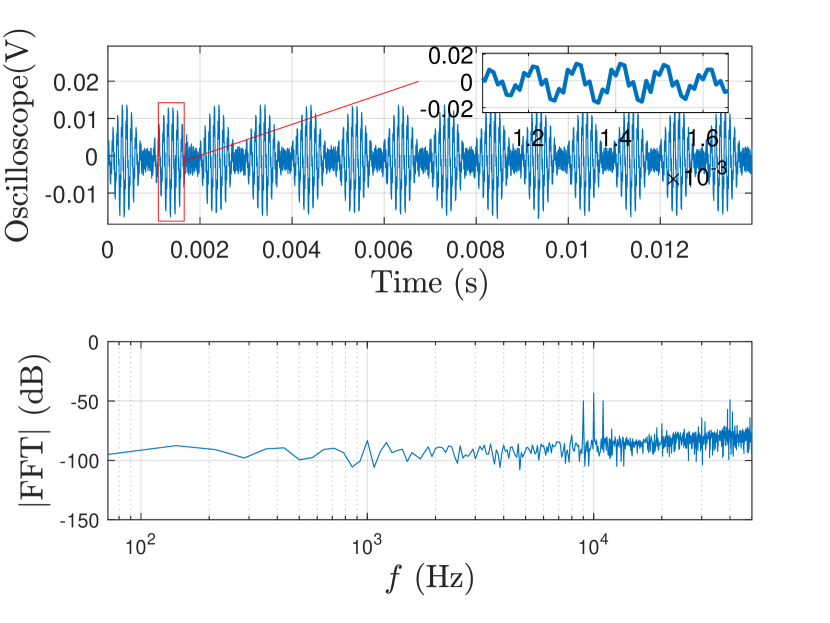
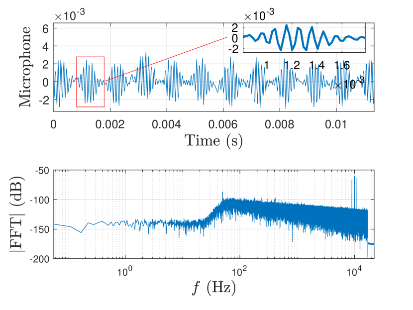
We demonstrate how our algorithm can be used in a realistic setup using a Motorola XT1541 Moto G3 smartphone. We inject amplitude-modulated signals using a Rohde & Schwarz SMC100A/B103 generator into the headphone jack of the phone, following direct power injection (DPI) methodology [7]. We collect measurements of sample points per run using an “Audio Recorder” app, and record the data at a frequency of in a dimensionless range (AAC encoding). We first amplitude-modulate over using an output level of . This injection is demodulated well by the smartphone and has a “similarity” (see Appendix 0.A) of over compared to a pure tone. We call this example the “clean” waveform. The second injection, which we call the “distorted” waveform, uses , , and has a similarity of less than to the ideal tone. Example measurements of these signals and “ideal” signals (see below) are shown in Figure 4.
The algorithm first calculates the noise level using the reference signals. As expected, the error average is very close to 0 (usually less than ), while the standard deviation is noticeable at around . Taking the reference signals as the target signal , the critical selective thresholds are close to . In other words, even if the injected waveforms do not correspond to “pure” signals, the adversary can inject them with high fidelity: the system is not selectively secure against them with high probability.
We also tried two signals as the signal that the adversary is trying to inject: a pure sine wave, and an exponential of the same sine wave. The averages and standard deviations for the calculated thresholds over all combinations of and reference signals are shown in Table 3. As we would expect, the thresholds for the distorted waveform are much lower than the values for the clean waveform: the signal is distorted, so it is hard to inject an ideal signal. We also find that the exponential function is a better fit for the signal we are seeing, and can better explain the harmonics. Table 3 also includes the critical universal injection threshold based on the two waveform injections. This threshold is much higher for both waveforms, as injections disturb the ADC output sufficiently, even when the demodulated signal is not ideal.
| Waveform | Validation | Ideal Sine | ||
|---|---|---|---|---|
| Clean | ||||
| Distorted |
4.3 Universal Injections on a Smartphone
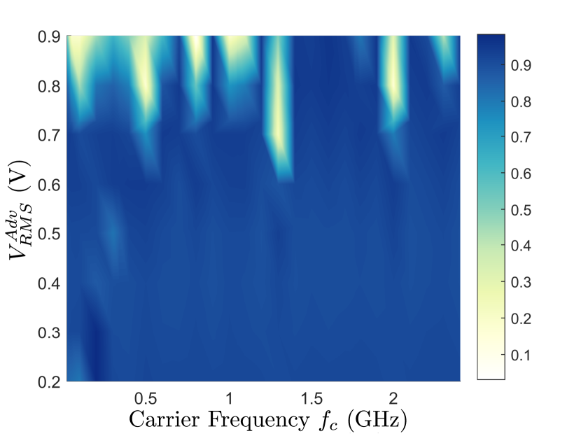
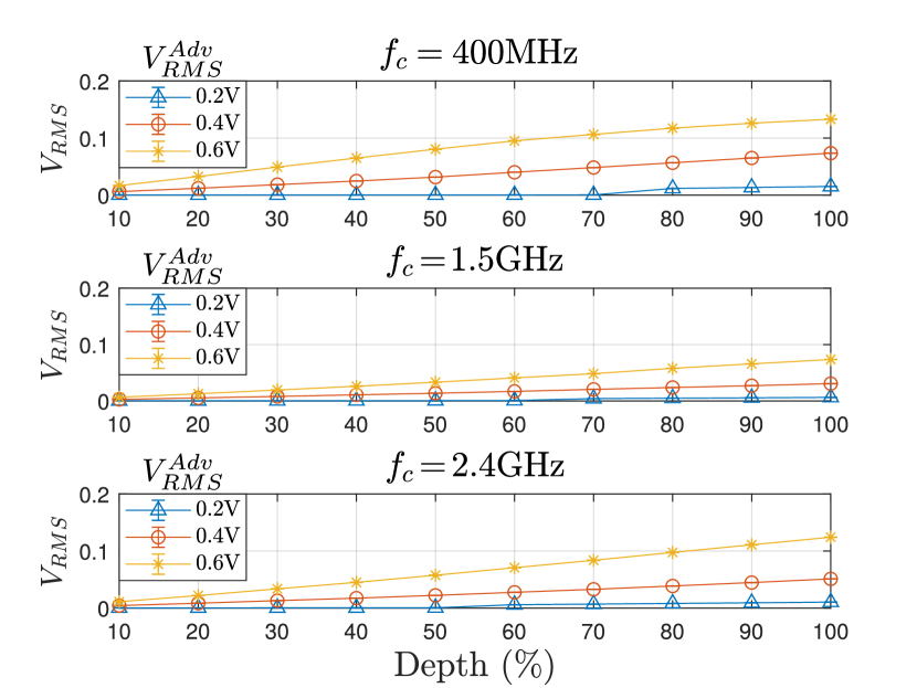
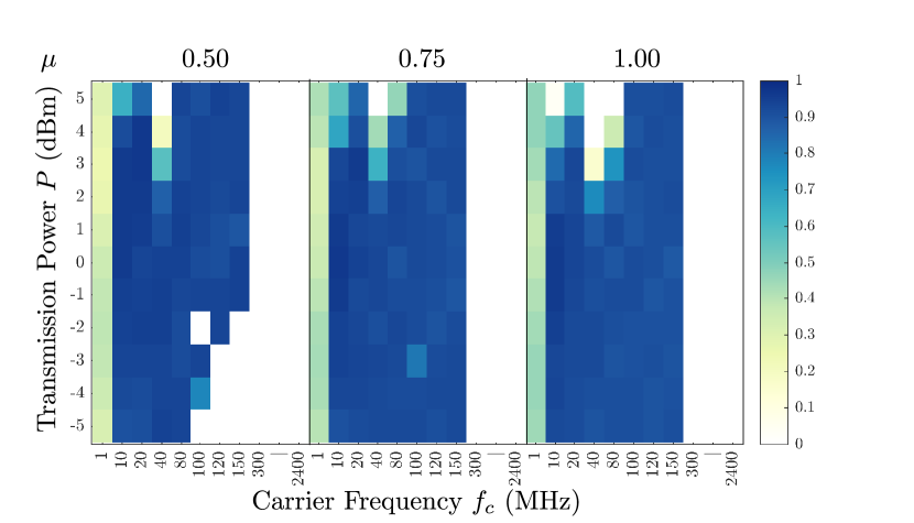
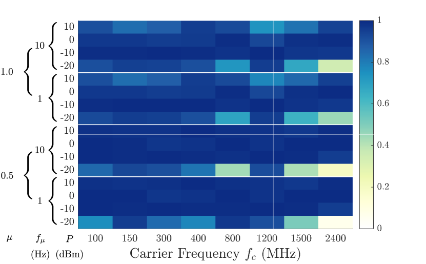
In this section, we demonstrate that the smartphone is vulnerable to the injection of arbitrary commands, which cause the smartphone to behave as if the user initiated an action. Using the same setup of direct power injection (Section 4.2), we first inject a modulated recording of “OK Google, turn on the flashlight” into the microphone port, checking both whether the voice command service was activated in response to “OK Google”, and whether the desired action was executed. We repeat measurements 10 times, each time amplitude-modulating the command at a depth of with on 26 carrier frequencies : , , and at a step of . The voice-activation feature (“OK Google”) worked with 100% success rate (10/10 repetitions) for all frequencies, while the full command was successfully executed for 23 of the 26 frequencies we tested (all frequencies except ). Increasing the output level to , increased success rate to 25/26 frequencies. Only did not result in a full command injection, possibly because the Wi-Fi disconnected in the process.
We repeated the above injections, testing 5 further commands to (1) call a contact; (2) text a contact; (3) set a timer; (4) mute the volume; and (5) turn on airplane mode. The results remained identical, regardless of the actual command to be executed. As a result, all carrier frequencies which are not severely attenuated by (e.g., when coupling to the user’s headphones) are vulnerable to injections of complex waveforms such as human speech.
5 Commercial ADC Response to Malicious Signals
| ADC | Manufacturer | Package | Type | Bits | Max | ||
|---|---|---|---|---|---|---|---|
| TLC549 | Texas Instruments | DIP | SAR | 8 | |||
| ATmega328P | Atmel | Integrated | SAR | 10 | |||
| Artix7 | Xilinx | Integrated | SAR | 12 | |||
| AD7276 | Analog Devices | TSOT | SAR | 12 | |||
| AD7783 | Analog Devices | TSSOP | 24 | [,] | |||
| AD7822 | Analog Devices | DIP | Flash | 8 |
As explained in Section 2, an adversary trying to inject signals remotely into a system typically needs to transmit modulated signals over high-frequency carriers. As is unique to each circuit and needs to be re-calculated even for minor changes to its components and layout [6], the first step to determine the system vulnerability is to understand the behavior of the ADC used.
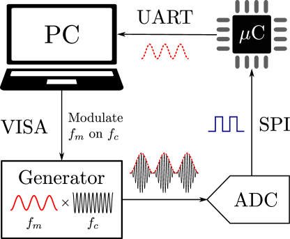
To do so, we inject signals into the ADCs to determine their demodulation characteristics. As shown in Figure 5, the output of the Rohde & Schwarz signal generator is directly connected to the ADC under test, while additional experiments with an amplifier or with remote transmissions are performed in Appendix 0.A. An Arduino Uno (ATmega328P microcontroller) interfaces with the ADC over the appropriate protocol, while a computer collects the measurements from the microcontroller over the UART, and controls the signal generator over the VISA interface.
Experiments are conducted with six ADCs from four manufacturers (Texas Instruments, Analog Devices, Atmel, and Xilinx) in different packages: some are part of the silicon in other ICs, while others are standalone surface-mount or through-hole chips. Delta-Sigma (), half-flash, and successive approximation (SAR) ADCs are tested, with sampling rates ranging from a few to several , and resolutions between and bits. Table 4 shows these properties along with the cutoff frequency , calculated using the parameters in the ADCs’ datasheets.
We use sinusoidals of frequencies that have been amplitude-modulated on carrier frequencies . In other words, we consider the intended signal to be , the sensor signal to be absent (), and evaluate how “close” is to the ADC output . We summarize typical results for each ADC here, and present more details in Appendix 0.A.
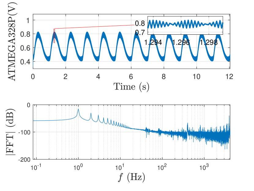
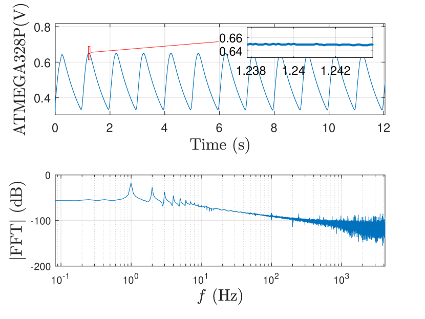
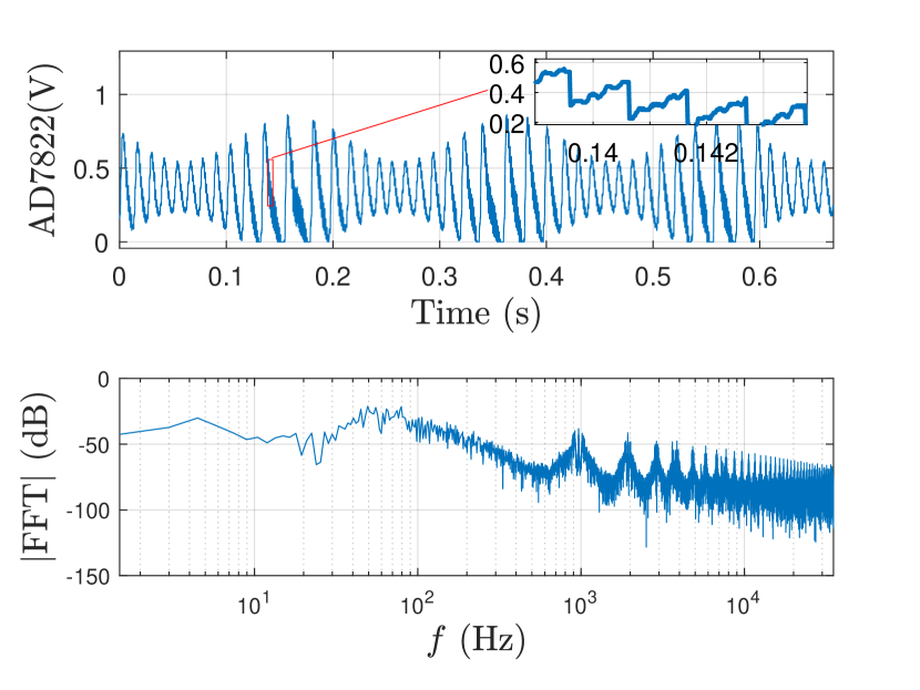
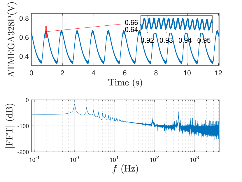
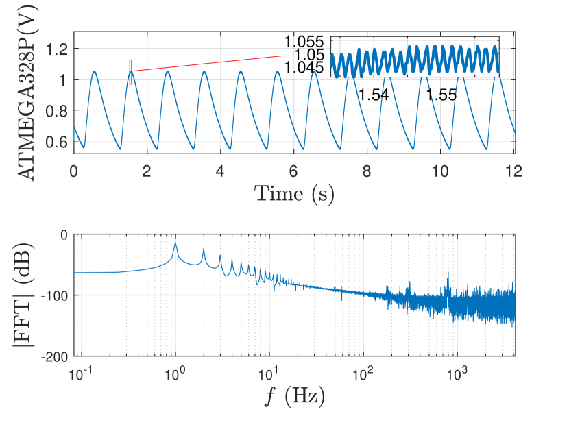
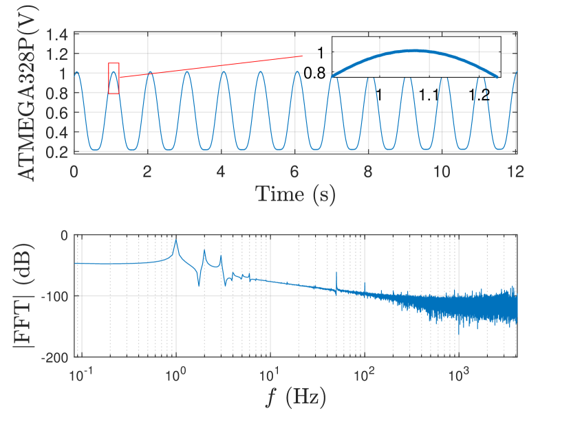
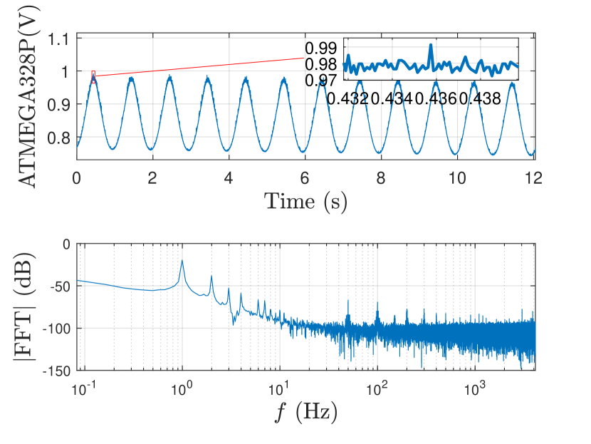
ATmega328P. Figure 6 presents two example measurements of outputs of the ATmega328P, both in the time domain and in the frequency domain. The input to the ADC is a signal modulated over different high-frequency carriers. As shown in the frequency domain (bottom of Figure 6), the fundamental frequency dominates all other frequencies, so the attacker is able to inject a signal of the intended frequency into the output of the ADC. However, the output at both carrier frequencies has strong harmonics at , which indicates that the resulting signal is not pure. Moreover, there is a residual high-frequency component, which is attenuated as the carrier frequency increases. Finally, there is a frequency-dependent DC offset caused, in part, by the ESD diodes, while the peak-to-peak amplitude of the measured signal decreases as the carrier frequency increases. This is due to the low-pass filtering behavior of the sample-and-hold mechanism, which also explains why we are only able to demodulate signals for carrier frequencies until approximately .

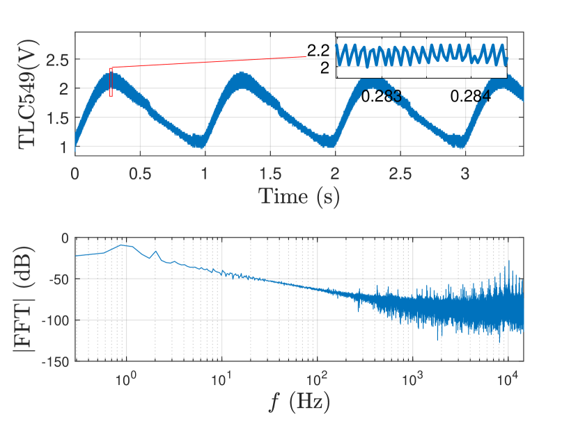
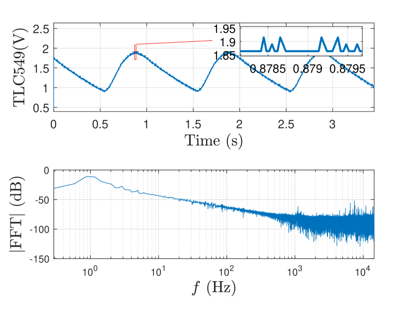
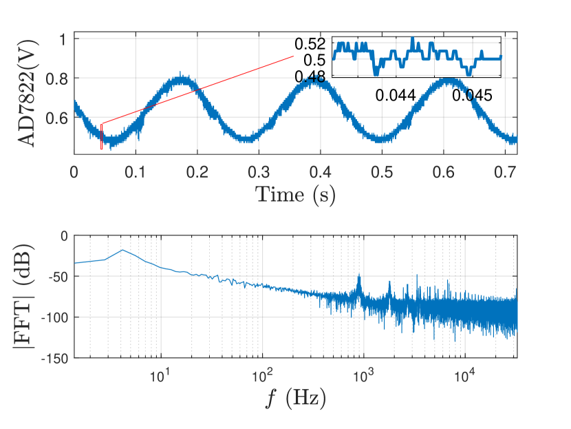
TLC549. The TLC549 (Figure 7(a)) also demodulates the injected signal, but still contains harmonics and a small high-frequency component.
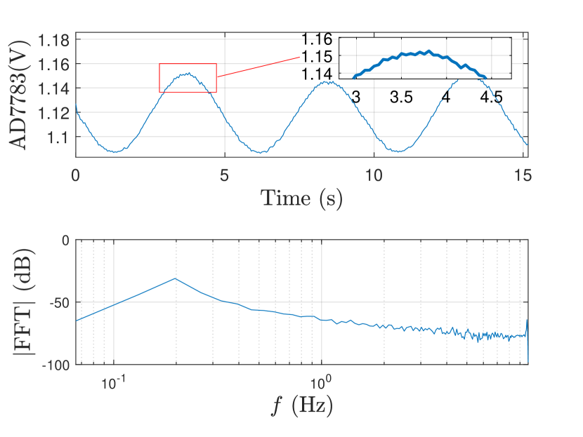
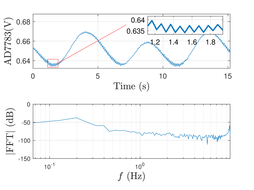
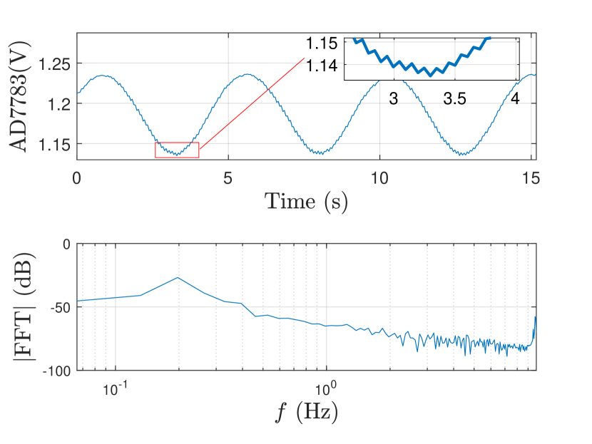
AD7783. As the AD7783 (Figure 7(b)) only has a sampling frequency of , aliasing occurs when the baseband signal exceeds the Nyquist frequency . For example, when the baseband frequency is , the fundamental frequency dominating the measurements is of frequency , with a high-frequency component of .
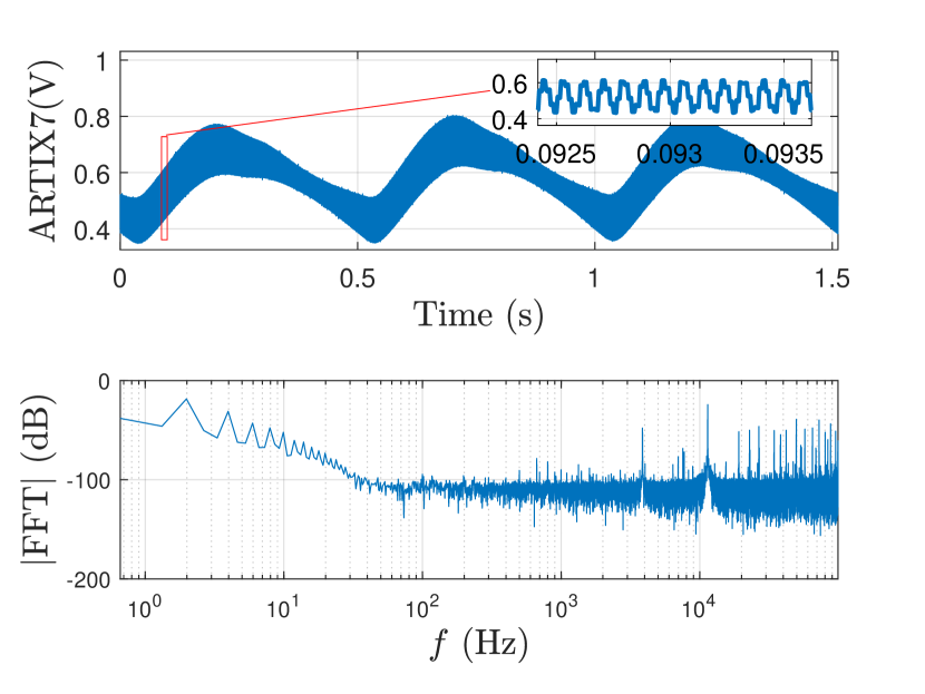
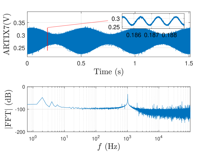
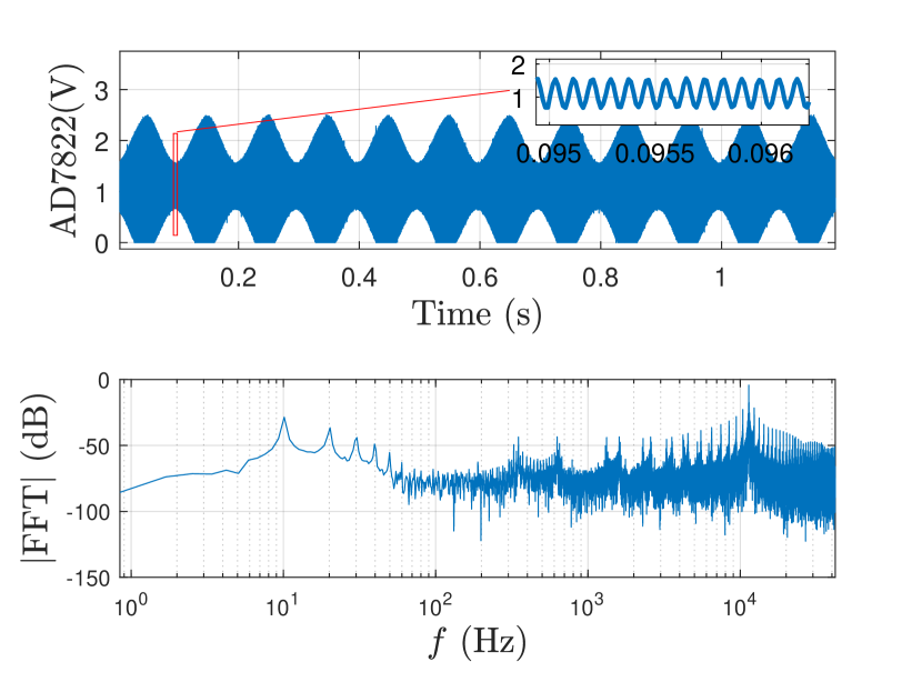
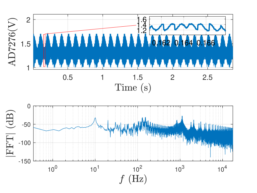
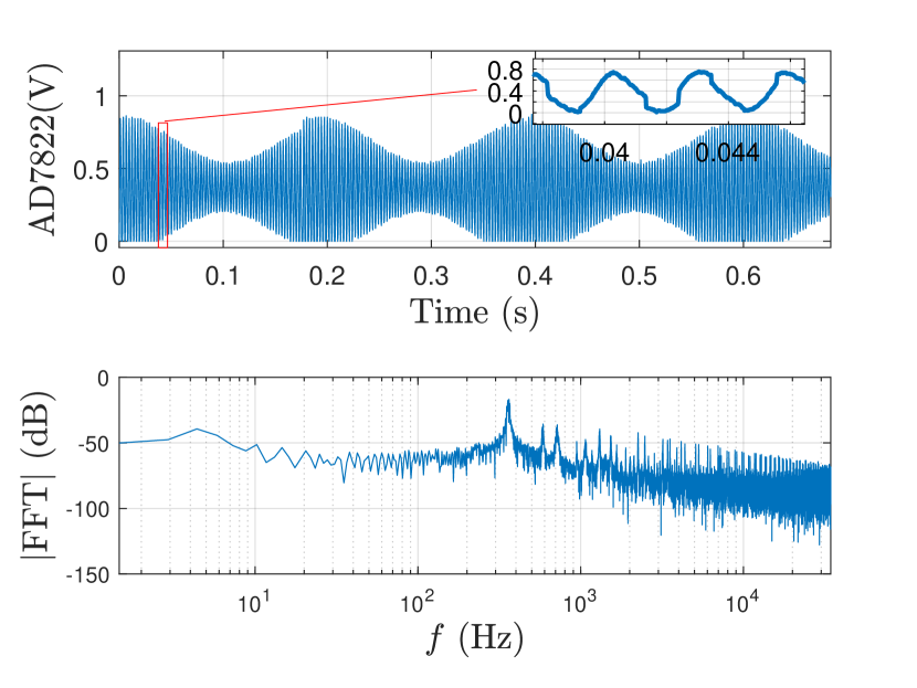
AD7822, AD7276, Artix7. The three remaining ADCs contain strong high-frequency components which dominate the low-frequency signal. Their outputs appear to be AM-modulated, but at a carrier frequency which is below the ADC’s Nyquist frequency. However, with manual tuning of the carrier frequency, it is possible to remove this high frequency component, causing the ADC to demodulate the input. This is shown for the Flash ADC AD7822 in Figure 8, where we change the carrier frequency in steps of .
Conclusion. The results of our experiments lead to the following observations:
-
1.
Generality – All 6 ADCs tested are vulnerable to signal injections at multiple carrier frequencies, as they demodulate signals, matching the theoretical expectations of Section 2.1. As the ADCs are of all major types and with a range of different resolutions and sampling frequencies, the conclusions drawn should also be valid for other ADC chips.
-
2.
Low-Pass Filter – Although all ADCs exhibited low-pass filtering characteristics, the maximum vulnerable carrier frequency for a given power level was multiple times the cut-off frequency of the circuit at the input of the ADC. This extended the frequency range that an attacker could use for transmissions to attack the system.
-
3.
Power – The adversary needs to select the power level of transmissions carefully: too much power in the input of the ADC can cause saturation and/or clipping of the measured signal. Too little power, on the other hand, results in output that looks like noise or a zero signal.
-
4.
Carrier Frequency – Some ADCs were vulnerable at any carrier frequency that is not severely attenuated by the sample-and-hold mechanism. For others, high-frequency components dominated the intended baseband signal of frequency in the ADC output for most frequencies. Even then, carefully-chosen carrier frequencies resulted in a demodulated ADC output.
6 Discussion
We now discuss how our work can inform design choices. To start, choosing the right ADC directly impacts the susceptibility to signal injection attacks. As shown in Section 5, some ADCs distort the demodulated output and result in more sawtooth-like output, making them more resilient to clean sinusoidal injections. Moreover, other ADCs require fine-grained control over the carrier frequency of injection. As the adversarial signal is transformed through the circuit-specific transfer function , the adversary may not have such control, resulting in a more secure system.
Having chosen the appropriate ADC based on cost, performance, security, or other considerations, a designer needs to assess the impact of . Prior work has shown that even small layout or component changes affect the EMI behavior of a circuit [6, 13, 23]. Since the ADC behavior can be independently determined through direct power injections, fewer experiments with remote transmissions are required to evaluate the full circuit behavior and how changes in the circuit’s topology influence the system’s security.
Our selective security definition and algorithm address how to determine the vulnerability of a system against specific waveforms. Universal security, on the other hand, allows us to directly compare the security of two systems for a fixed adversarial voltage budget through their critical universal security thresholds. Moreover, given a probability/threshold , we can calculate the critical universal voltage level, which is the maximum output level for which a system is still universally -secure.
Our smartphone case study showed that our framework can be used in practice with real systems, while our “OK Google” experiments demonstrated that less-than-perfect injections of adversarial waveforms can have the same effect as perfect injections. This is because there is a mismatch between the true noise level of a system and the worst-case noise level that the system expects. In other words, injections worked at all carrier frequencies, even when the demodulated output was noisy or distorted. This is a deliberate, permissive design decision, which allows the adversary to succeed with a range of different and noisy waveforms , despite small amplitudes and DC offsets.
Although not heavily discussed in this paper, our model and definitions are general enough to capture alternative signal injection techniques. For instance, electro-mechanical sensors have resonant frequencies which allow acoustic injection attacks [22, 25]. can account for such imperfections in the sensors themselves, attenuating injection frequencies which are not close to the resonant frequencies. Our system model also makes it easy to evaluate countermeasures and defense mechanisms in its context. For example, shielding increases the attenuation factor of , thereby increasing the power requirements for the adversary (Section 2.1). Alternatively, a low-pass filter (LPF) before the ADC and/or amplifier changes , and attenuates the high-frequency components which would induce non-linearities. Note, however, that even moving the pre-amplifier, LPF and ADC into the same IC package does not fully eliminate the vulnerability to signal injection attacks (Section 7) as the channel between the analog sensor and the ADC cannot be fundamentally authenticated.
7 Related Work
Ever since a 2013 paper by Kune et al. showed that electromagnetic (EM) signals can be used to cause medical devices to deliver defibrillation shocks [10], there has been a rise in EM, acoustic, and optical signal injection attacks against sensor and actuator systems [7]. Although some papers have focused on vulnerabilities caused by the ADC sampling process itself [2], others have focused on exploiting the control algorithms that make use of the digitized signal. For example, Shoukry et al. showed how to force the Anti-Lock Braking Systems (ABS) to model the real input signal as a disturbance [20]. Selvaraj et al. also used the magnetic field to perform attacks on actuators, but further explored the relationship between frequency and the average injected voltage into ADCs [19]. By contrast, our paper primarily focused on a formal mathematical framework to understand security in the context of signal injection attacks, but also investigated the demodulation properties of different ADCs.
Our work further highlighted how to use the introduced algorithm and definitions to investigate the security of a smartphone, complementing earlier work which had shown that AM-modulated electromagnetic transmissions can be picked up by hands-free headsets to trigger voice commands in smartphones [9]. Voice injection attacks can also be achieved by modulating signals on ultrasound frequencies [27], or by playing two tones at different ultrasound frequencies and exploiting non-linearities in components [18]. Acoustic transmissions at a device’s resonant frequencies can also incapacitate [22] or precisely control [24] drones, with attackers who account for sampling rate drifts being able to control the outputs of accelerometers for longer periods of time [25]. Moreover, optical attacks can be used to spoof medical infusion pump measurements [14], and cause autonomous cars and unmanned aerial vehicles (UAVs) to drift or fail [3, 16, 26].
It should be noted that although the literature has primarily focused on signal injection attacks, some works have also proposed countermeasures. These defense mechanisms revolve around better sampling techniques, for example by adding unspoofable physical and computational delays [21], or by oversampling and selectively turning the sensors off using a secret sequence [28].
Overall, despite the extensive literature on signal injection attacks and defenses, the setup and effectiveness of different works is often reported in an inconsistent way, making their results hard to compare [7]. Our work, recognizing this gap, introduced a formal foundation to define and quantify security against signal injection attacks, working towards unifying the reporting methodology for competing works.
8 Conclusion
Sensors guide many of our choices, and we often blindly trust their values. However, it is possible to spoof their outputs through electromagnetic or other signal injection attacks. To address the lack of a unifying framework describing the susceptibility of devices to such attacks, we defined a system and adversary model for signal injections. Our model is the first to abstract away from specific environments and circuit designs and presents a strong adversary who is only limited by transmission power. It also makes it easy to discuss and evaluate countermeasures in its context and covers different types of signal injection attacks.
Within our model, we defined existential, selective, and universal security, capturing effects ranging from mere disruptions of the ADC outputs to precise injections of all waveforms. We showed that our definitions can be used to evaluate the security level of an off-the-shelf smartphone, and introduced an algorithm to calculate “critical” thresholds, which express how close an injected signal is to the ideal signal. Finally, we characterized the demodulation characteristics of commercial ADCs to malicious injections. In response to the emerging signal injection threat, our work paves the way towards a future where security can be quantified and compared through our methodology and security definitions.
References
- [1] Benesty, J., Chen, J., Huang, Y.: On the importance of the Pearson correlation coefficient in noise reduction. IEEE Transactions on Audio, Speech, and Language Processing 16(16), 757–765 (2008)
- [2] Bolshev, A., Larsen, J., Krotofil, M., Wightman, R.: A rising tide: Design exploits in industrial control systems. In: USENIX Workshop on Offensive Technologies (WOOT) (2016)
- [3] Davidson, D., Wu, H., Jellinek, R., Singh, V., Ristenpart, T.: Controlling UAVs with sensor input spoofing attacks. In: USENIX Workshop on Offensive Technologies (WOOT) (2016)
- [4] Friis, H.T.: A note on a simple transmission formula. Proceedings of the IRE (JRPROC) 34(5), 254–256 (May 1946)
- [5] Fu, K., Xu, W.: Risks of trusting the physics of sensors. Commun. ACM 61(2), 20–23 (2018)
- [6] Gago, J., Balcells, J., González, D., Lamich, M., Mon, J., Santolaria, A.: EMI susceptibility model of signal conditioning circuits based on operational amplifiers. IEEE Transactions on Electromagnetic Compatibility 49(4), 849–859 (2007)
- [7] Giechaskiel, I., Rasmussen, K.B.: Taxonomy and challenges of out-of-band signal injection attacks and defenses. IEEE Communications Surveys & Tutorials (COMST) (2020)
- [8] Goldwasser, S., Micali, S., Rivest, R.L.: A digital signature scheme secure against adaptive chosen-message attacks. SIAM Journal on Computing 17(2), 281–308 (1988)
- [9] Kasmi, C., Lopes-Esteves, J.: IEMI threats for information security: Remote command injection on modern smartphones. IEEE Transactions on Electromagnetic Compatibility 57(6), 1752–1755 (2015)
- [10] Kune, D.F., Backes, J.D., Clark, S.S., Kramer, D.B., Reynolds, M.R., Fu, K., Kim, Y., Xu, W.: Ghost talk: Mitigating EMI signal injection attacks against analog sensors. In: IEEE Symposium on Security and Privacy (S&P) (2013)
- [11] Lena, P.D., Margara, L.: Optimal global alignment of signals by maximization of Pearson correlation. Information Processing Letters 110(16), 679–686 (2010)
- [12] Leone, M., Singer, H.L.: On the coupling of an external electromagnetic field to a printed circuit board trace. IEEE Transactions on Electromagnetic Compatibility 41(4), 418–424 (1999)
- [13] Lissner, A., Hoene, E., Stube, B., Guttowski, S.: Predicting the influence of placement of passive components on EMI behaviour. In: European Conference on Power Electronics and Applications (2007)
- [14] Park, Y.S., Son, Y., Shin, H., Kim, D., Kim, Y.: This ain’t your dose: Sensor spoofing attack on medical infusion pump. In: USENIX Workshop on Offensive Technologies (WOOT) (2016)
- [15] Pelgrom, M.J.M.: Analog-to-Digital Conversion. Springer Publishing Company, Incorporated, 3rd edn. (2017)
- [16] Petit, J., Stottelaar, B., Feiri, M., Kargl, F.: Remote attacks on automated vehicles sensors: Experiments on camera and LiDAR. Black Hat Europe (2015)
- [17] Redouté, J.M., Steyaert, M.: EMC of Analog Integrated Circuits. Springer Publishing Company, Incorporated, 1st edn. (2009)
- [18] Roy, N., Hassanieh, H., Roy Choudhury, R.: BackDoor: Making microphones hear inaudible sounds. In: International Conference on Mobile Systems, Applications, and Services (MobiSys) (2017)
- [19] Selvaraj, J., Dayanikli, G.Y., Gaunkar, N.P., Ware, D., Gerdes, R.M., Mina, M.: Electromagnetic induction attacks against embedded systems. In: Asia Conference on Computer and Communications Security (ASIACCS) (2018)
- [20] Shoukry, Y., Martin, P.D., Tabuada, P., Srivastava, M.B.: Non-invasive spoofing attacks for anti-lock braking systems. In: Cryptographic Hardware and Embedded Systems (CHES) (2013)
- [21] Shoukry, Y., Martin, P.D., Yona, Y., Diggavi, S., Srivastava, M.B.: PyCRA: Physical challenge-response authentication for active sensors under spoofing attacks. In: Conference on Computer and Communications Security (CCS) (2015)
- [22] Son, Y., Shin, H., Kim, D., Park, Y., Noh, J., Choi, K., Choi, J., Kim, Y.: Rocking drones with intentional sound noise on gyroscopic sensors. In: USENIX Security Symposium (2015)
- [23] Sutu, Y.H., Whalen, J.J.: Statistics for demodulation RFI in operational amplifiers. In: International Symposium on Electromagnetic Compatibility (EMC) (1983)
- [24] Trippel, T., Weisse, O., Xu, W., Honeyman, P., Fu, K.: WALNUT: Waging doubt on the integrity of MEMS accelerometers with acoustic injection attacks. In: IEEE European Symposium on Security and Privacy (EuroS&P) (2017)
- [25] Tu, Y., Lin, Z., Lee, I., Hei, X.: Injected and delivered: Fabricating implicit control over actuation systems by spoofing inertial sensors. In: USENIX Security Symposium (2018)
- [26] Yan, C., Xu, W., Liu, J.: Can you trust autonomous vehicles: Contactless attacks against sensors of self-driving vehicle. DEFCON (2016)
- [27] Zhang, G., Yan, C., Ji, X., Zhang, T., Zhang, T., Xu, W.: DolphinAttack: Inaudible voice commands. In: Conference on Computer and Communications Security (CCS) (2017)
- [28] Zhang, Y., Rasmussen, K.B.: Detection of electromagnetic interference attacks on sensor systems. In: IEEE Symposium on Security and Privacy (S&P) (2020)
Appendix 0.A Additional Experiments with ADCs
This appendix contains further measurements on the demodulation properties of ADCs. Section 0.A.1 precisely defines the similarity metric of Section 4, and validates the experimental setup. Section 0.A.2 and 0.A.3 then conduct further characterization experiments of the smartphone microphone and ATmega328P ADC respectively. Finally, Section 0.A.4 contains additional examples of the demodulation characteristics of the remaining ADCs.
0.A.1 Similarity Metric and Setup Validation
The experiments of Section 4.2 required an independent metric to evaluate how “similar” two signals are as a way of independently validating the security definitions of Section 3. The metric proposed for this task is based on the Pearson Correlation Coefficient (PCC), which is commonly found in signal-alignment and optimization applications [1, 11]. It is defined as the covariance of two variables divided by the product of their standard deviations:
| (6) |
It is a suitable metric because it removes the mean value of the signals (DC shift), as well as the effects of scaling (related to transmission power). In other words, for a variable and scalars . However, the PCC is sensitive to signal alignment. To overcome this issue, the phase (time) offset between two signals , can be found using cross-correlation. Specifically, the signals are aligned when the cross-correlation coefficient is maximized:
| (7) |
Using Equations (6) and (7), the similarity metric between the measured signal and the ideal signal can be defined as follows:
| (8) |
To sanity-check this metric and the experimental setup, an unmodulated signal is generated. Figure 9(a) shows this waveform as measured by the smartphone of Section 4.2 along with an ideal signal. Even though the amplitudes are different, the frequency responses of the measured and the ideal signal are almost identical, with the two signals having a similarity of according to Equation (8).
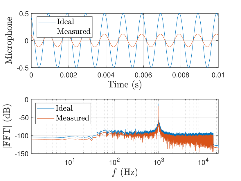
Figures 9(b) and 9(c) additionally show the same signal modulated on a carrier frequency of at a depth of . This carrier frequency was chosen as it is within the Nyquist range of the smartphone ADC (sampling frequency ). Figure 9(b) contains measurements taken by a Rigol DS2302A oscilloscope with a timescale division of , while Figure 9(c) uses the smartphone microphone.
Unlike the examples of Section 4, the measurements shown in Figure 9 do not exhibit harmonics, but rather high-frequency components at and , as expected. Consequently, the demodulation characteristics are due to non-linearities in amplifiers and ADCs when used outside of their intended range, instead of the experimental setup.
0.A.2 Smartphone Microphone Properties
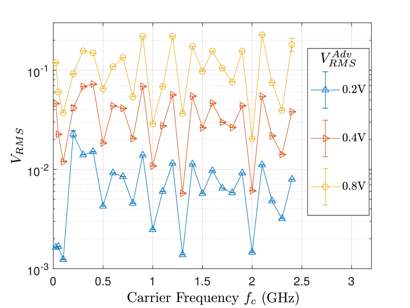
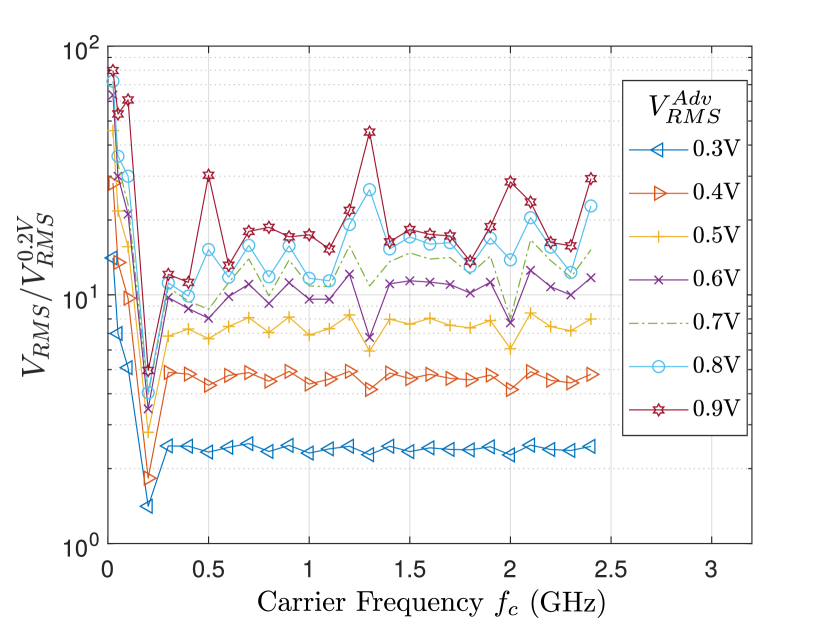
This section characterizes the smartphone microphone through the direct injection methodology of Section 5. An tone is amplitude-modulated with a depth of on the following carrier frequencies : , , and at a step of . The RMS output level of the signal generator is also varied between at a step of .
The similarity of the measured to the ideal signal for various carrier frequencies and output levels is shown in Figure 10(a). It is consistently high for all frequencies when , while higher voltage levels lead to more pronounced harmonics and clipping, reducing the similarity. The results are consistent across measurements: the confidence interval of the similarity is always below , except for the pairs and , where it reaches .
According to work on amplifier properties [23], the measured RMS voltage level , the input voltage , the modulation depth , the signal frequency , and the carrier frequency satisfy the following relationship:
| (9) |
where is a second-order transfer function. Figure 10 mostly confirms this equation for the microphone and ADC subsystem of the smartphone.
Specifically, fixing and in Equation (9) suggests that across all carrier frequencies . Indeed, Figure 10(b) verifies that the received RMS voltage is linear in the modulation depth for fixed with . For , the relationship becomes linear after , as the measured is approximately below that.
Figure 10(c) illustrates that the transfer function for the response is frequency-dependent. Finally, Figure 10(d) shows relative to . For and , there is a linear relationship between the carrier frequency and , as predicted by Equation (9).
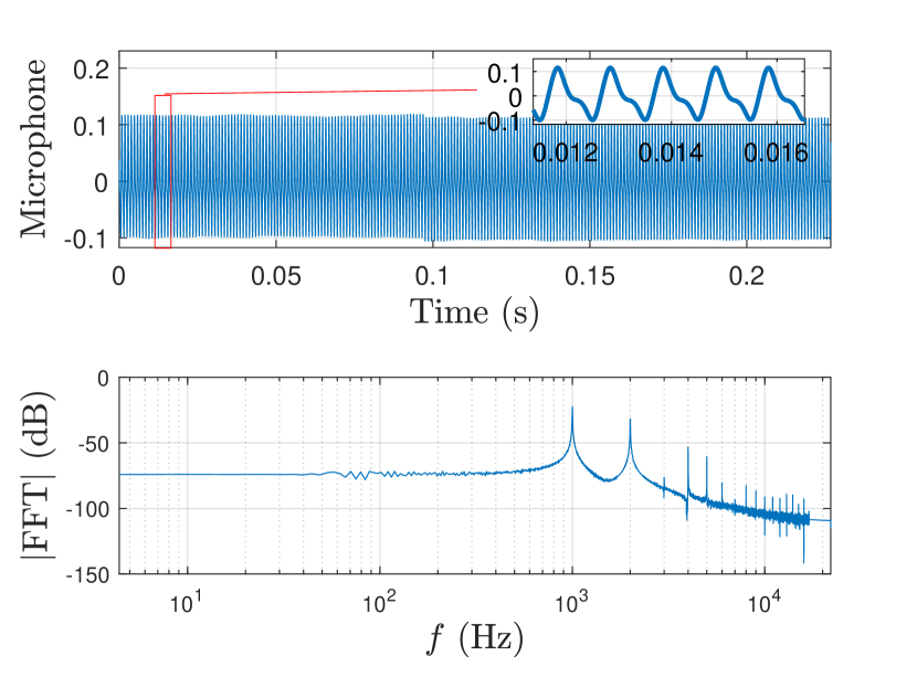
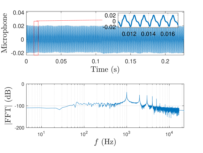
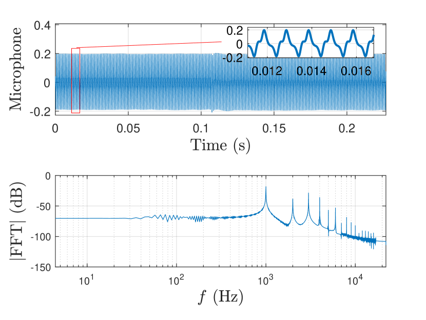
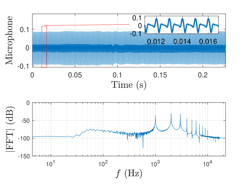
Figure 11 shows example microphone outputs for different carrier frequencies and output voltages . They all exhibit high harmonics, but the similarity compared to the ideal signal for Figures 11(a)–11(c) is still over . However, the injection of Figure 11(d) contains more pronounced distortions, and the similarity drops to less than .
Overall, the results of this section show that a higher-order transfer function may be needed to more accurately predict the ADC output, both in terms of its RMS voltage, and in terms of the harmonics it produces.
0.A.3 ATmega328P Characterization
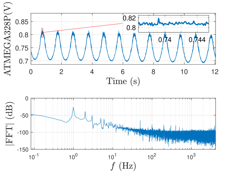
This section contains detailed results for injections into the ATmega328P ADC in three different arrangements: (a) the ADC on its own; (b) the ADC with an amplifier; and (c) the ADC with an amplifier and an antenna. The experimental results support the theoretical model of Section 2 and show that, despite its low-pass filtering behavior, the ADC demodulates signals carried at frequencies multiple times the cut-off frequency of the sample-and-hold mechanism. Moreover, external amplifier non-linearities increase the vulnerable frequency band into the range.
ATmega328P Only. The first experiment targets the ATmega328P directly, without using any additional components. The similarity of the demodulated signal to the ideal signal is calculated for injections at different powers , modulation depths , carrier frequencies , and a signal frequency of . As Figure 12(a) illustrates, the similarity for is always low due to aliasing. However, similarity is high for between , but signals are severely attenuated for . Small modulation depths and powers do not result in demodulated outputs, while too much power causes the ADC to be saturated. This leads to partial clipping of the signal, or induces a DC offset which is beyond the range of the ADC. Overall, the adversary has a range of choices for and , and can use carrier frequencies which are multiple times the cutoff frequency of the ADC, provided these are not attenuated by the circuit-specific transfer function .
ATmega328P + Amplifier. A low-cost, off-the-shelf wideband LNA is added before the input to the ADC to change the transfer function . The amplifier works between and can perform a maximum amplification of . It can output at most , and has a noise figure of approximately . Sinusoidals of and are modulated at depths of on carrier frequencies from to at transmission powers between and . As can be seen in Figure 13(a), the similarity is high across all frequencies, provided the transmission power is above a minimum threshold.
The amplifier thus both reduces the power requirements for the adversary, and increases the vulnerable frequencies to the range. This allows an attacker to target systems with short wires between the ADC and the sensor with a lower power budget: short wires are not a sufficient defense against electromagnetic out-of-band signal injection attacks. Moreover, it should be noted that an adversary gains an advantage by not obeying the amplifier constraints: abusing the amplifier by transmitting higher-powered signals or by driving frequency signals outside of the intended range still results in recognizable output. In other words, although the signal may be distorted, non-linearities produce outputs within the range of the ADC.
ATmega328P + Amplifier + Antenna. The final set of experiments changes the circuit-specific transfer function by using a transmitting antenna at the signal generator output and a receiving antenna at the amplifier input. The antennas used are Ettus Research omnidirectional VERT400 antennas, which are resonant at , , and . The antennas are placed in parallel at a distance of to one another, and the results for sine signals of and are presented in Figure 13(b). Although the minimum power required for successful injections is higher due to transmission losses, the system remains vulnerable for all three frequencies due to the amplifier and ADC non-linearities. In other words, results are reproducible across multiple setups, whether through remote transmissions, or through direct injections with an identity transfer function .
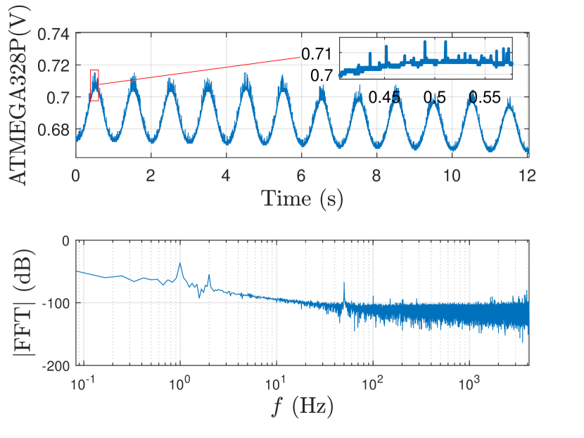
Figures 14–16 show example outputs from the internal ATmega328P ADC for different carrier frequencies , powers , and modulation depths , with fixed at . Figure 14 first shows the results for the ADC on its own, and complements Figure 6 of Section 5. Although harmonics of the fundamental persist, the high-frequency component becomes less pronounced as increases.
Figure 15 then shows output from the ATmega328P for two different carrier frequencies when connected to an amplifier. The ADC no longer behaves like a low-pass filter due to non-linearities, while harmonics of the fundamental remain strong. Finally, Figure 16 shows output from the ATmega328P for remote injections using the VERT400 antenna with the amplifier. As in the amplifier case, carrier frequencies in the range are still demodulated, and harmonics (and some high-frequency components) persist.
0.A.4 Further ADC Demodulation Examples
This section contains additional examples of injections into the different ADCs.
TLC549. Figure 17 shows example outputs from the TLC549 ADC for two carrier frequencies . Harmonics of the fundamental are not pronounced, as the resolution is only 8 bits.
Artix 7. Figure 18 shows example outputs from the Artix 7 ADC for two carrier frequencies . The output contains high-frequency components which dominate the target signal, forcing injections to require more fine-grained control over the carrier frequency.
AD7783. Figure 19 shows the output from the (slow) AD7783 ADC for different carrier frequencies and modulation depths. As is above the Nyquist frequency, aliasing occurs. The strongest frequency present is , while the high-frequency component is .
AD7822 & AD7276. Figure 20(a) and Figure 20(b) show example measurements for the AD7822 and the AD7276 ADCs respectively. As for the Artix 7, high-frequency components dominate the output, and hence require manual tuning to get a demodulated, low-frequency output.