Current address: ]Centre of Excellence for Quantum Computation and Communication Technology, University of New South Wales, Sydney, New South Wales 2052, Australia
Current address: ]National Graphene Institute, University of Manchester, Manchester, M13 9PL, UK
Current address: ]Instituto de Sistemas Optoelectrónicos y Microtecnología, Universidad Politécnica de Madrid, Madrid 28040, Spain
Current address: ]University of California, San Francisco, 185 Berry Street Bldg B, San Francisco CA 94158, USA
Current address: ]Department of Electronic and Electrical Engineering, University of Sheffield, Mappin St, Sheffield, S1 3JD, UK
Single-photon Emission from an Acoustically-driven Lateral Light-emitting Diode
Abstract
Single-photon sources are essential building blocks in quantum photonic networks, where quantum-mechanical properties of photons are utilised to achieve quantum technologies such as quantum cryptography and quantum computing. Most conventional solid-state single-photon sources are based on single emitters such as self-assembled quantum dots, which are created at random locations and require spectral filtering. These issues hinder the integration of a single-photon source into a scaleable photonic quantum network for applications such as on-chip photonic quantum processors. In this work, using only regular lithography techniques on a conventional GaAs quantum well, we realise an electrically triggered single-photon source with a GHz repetition rate and without the need for spectral filtering. In this device, a single electron is carried in the potential minimum of a surface acoustic wave (SAW) and is transported to a region of holes to form an exciton. The exciton then decays and creates a single photon in a lifetime of ps. This SAW-driven electroluminescence (EL) yields photon antibunching with , which satisfies the common criterion for a single-photon source . Furthermore, we estimate that if a photon detector receives a SAW-driven EL signal within one SAW period, this signal has a 79%–90% chance of being a single photon. This work shows that a single-photon source can be made by combining single-electron transport and a lateral n-i-p junction. This approach makes it possible to create multiple synchronised single-photon sources at chosen positions with photon energy determined by quantum-well thickness. Compared with conventional quantum-dot-based single-photon sources, this device may be more suitable for an on-chip integrated photonic quantum network.
The development of single-photon sources is important for many quantum information technologies (Senellart2017, ; Aharonovich2016, ; Shields2007, ), such as quantum cryptography (Gisin2001, ; Ekert1991, ; Lo1999, ), quantum communication (Kimble2008, ; Pirandola2015, ; Horodecki2009, ), quantum metrology (Giovannetti2004, ; Giovannetti2011, ), and quantum computation (Knill2001, ; Kok2007, ). Currently, most high-performance single-photon sources are self-assembled InGaAs-based quantum dots (QDs) (He2013, ; Somaschi2016, ; Ding2016, ). However, there are several issues that may limit their integration into practical quantum photonic networks (Politi2009, ; Crespi2011, ; Harris2017, ; Qiang2018, ; Spring2013, ; Wang2017, ; Sparrow2018, ; Arrazola2018, ). Firstly, in conventional growth of self-assembled QDs, the location and size of each QD are quite random. Therefore, one has to rely on statistics to create structures like optical cavities and gates around a quantum dot. This will be an issue for applications that require several deterministically-fabricated single-photon sources on a compact chip. Secondly, it is hard to precisely control the size of a quantum dot, which will affect the single-photon energy. Hence, it is challenging to make identical QD single-photon sources, which is essential for applications like quantum computation and a quantum repeater (Knill2001, ; Kaltenbaek2009, ). Finally, in order to ensure that a neutral exciton is created in every optical or electrical excitation, the excitation power is usually high, which causes extra biexciton emission line. This issue can be avoided by employing resonance fluorescence, which requires a more sophisticated tuneable light source to excite each dot (Ding2016, ), and needs orthogonal-excitation or cross-polarisation configurations to suppress the laser background (Ding2016, ; Muller2007, ; Ates2009, ).

On the other hand, many prototypical quantum processors, for tasks such as boson sampling, Shor’s algorithm, arbitrary two-qubit gates, and quantum molecular-dynamics simulation, have recently been realised using on-chip photonic quantum networks (Politi2009, ; Crespi2011, ; Harris2017, ; Qiang2018, ; Spring2013, ; Wang2017, ; Sparrow2018, ). In these works, multiple heralded single-photon states are prepared via spontaneous parametric down-conversion or spontaneous four-wave mixing, which both have low efficiency issue due to their Poissonian photon-number distribution (Migdall2002, ; Collins2013, ). Therefore, if a single-photon source, which exhibits sub-Poissonian photon statistics, can be fabricated just by conventional lithography techniques, it will be possible to make multiple sources at predefined locations on a photonic chip. Moreover, if these sources can be electrically triggered at a GHz-repetition rate, an ideal and compact photonic quantum processor may thus be achieved.
To try to overcome the issues of the randomness of self-assembled quantum dots and to create integrated on-chip photonic quantum networks, a single-photon source can in principle be made in a novel approach combining a single-electron-transport technique with a lateral n-i-p junction, a semiconductor interface between adjacent electron (‘n’) and hole (‘p’) regions, formed in a quantum well, with an intrinsic region (‘i’) in between (a lateral light-emitting diode). In recent years, control of a propagating single-electron quantum state has been achieved using an electron pump (Giblin2012, ), a leviton (Dubois2013, ), and a surface acoustic wave (SAW) (Shilton1996, ; PhysRevB.56.15180, ; Ford2017, ; Bauerle2018, ). If a single electron can be transported from an electron region into a region of holes (an n-i-p junction), it can form an exciton and then decay into a single photon. In this approach, the emission of single photons is caused by the single-electron transport, rather than the stochastic capture of electrons in a static quantum dot. Therefore, it does not suffer from the spectral and temporal randomness of self-assembled quantum-dots, and is possible to be made at any arbitrary location using conventional lithography techniques. Moreover, because only one exciton can be formed at a time using the single-electron-transport technique, a biexciton will not form in this approach, eliminating the need for extra spectral filtering. Furthermore, since the exciton energy is determined by the thickness of the quantum well, the single-photon energy can be easily predicted, which makes the optical-cavity integration more reliable.
Based on the approach mentioned above, a scheme for making a single-photon source using a SAW has been proposed (Foden2000, ). This makes use of the fact that, in a piezoelectric material such as GaAs, a SAW consists of both a strain and a potential modulation. In a narrow channel, electrons are confined in moving quantum dots formed by the SAW potential and the lateral channel potential. The number of electrons in each SAW potential minimum is well defined if the Coulomb charging energy is large enough. The SAW (of frequency ) can therefore drive a quantised current along the channel ( is the electronic charge) Shilton1996 ; Ford2017 . To generate light, single electrons must be carried in SAW potential minima across a lateral n-i-p junction to create single photons by recombining with holes (see Supplementary Video for a simple animation). Over more than a decade, various attempts have been made to implement this scheme (Hosey2004, ; Cecchini2005, ; Smith2006, ; Gell2006, ; DeSimoni2009, ; Dai2014, ). However, to the authors’ knowledge, no evidence for photon antibunching or single-photon emission has been observed. Note that a few works based on SAW-injected or SAW-regulated excitons in a QD have shown single-photon emission (Iikawa2009, ; Weib2016, ; Villa2017, ). However, they still rely on the presence of a QD and thus suffer from the randomness issue. Here we successfully demonstrate that an electrically triggered and GHz-repetition-rate single-photon source based on this scheme can be fabricated in a deterministic conventional lithography process, and, without any spectral filtering, our device shows clear photon antibunching with the second-order correlation function , which is lower than the common criterion for a single-photon source, .
In this work, the lateral n-i-p junction is made in a conventional undoped GaAs quantum well using standard lithography techniques (see Methods). Electrons and holes are induced in the regions under the electron and hole surface gates, which are separated by an intrinsic region (Fig. 1(a)). A source-drain (S-D) bias less than the GaAs bandgap is applied across the n-i-p junction to create a finite potential difference between the electron and hole regions. A SAW is generated by applying a radio-frequency (RF) signal to an interdigitated transducer (IDT) at its resonant frequency GHz. Electrons are trapped in SAW potential minima and pushed towards the hole region (Fig. 1(b)). To achieve SAW-driven single-electron transport, lateral confinement is provided by etching the region connecting the electron and hole regions into a 1D intrinsic channel. In addition, a pair of side gates is placed on either side of the channel to adjust the electrostatic potential in the intrinsic region. The physical length of the channel is made to be similar to the SAW wavelength of 2.5 m. In this case, any current flow will be caused by the SAW carrying electrons up the potential slope linking the conduction band in the regions of electrons and holes, not by the SAW reducing the height of the potential barrier in the intrinsic region at a certain part of its cycle. All measurements were carried out at 1.5 K.
In order to test the effect of a SAW on the induced lateral n-i-p junction, a S-D bias less than 1.45 V is applied to the junction. This is at least 90 mV below the voltage required to align the conduction band in the n and p regions so that current can flow at cryogenic temperature if any intermediate barrier is overcome. In this case, due to the conduction-band offset between the n and p regions, electrons cannot reach the p region to recombine with holes unless a SAW carries them there. Therefore, a S-D current and electroluminescence (EL) signal will only appear when an RF signal is applied to the IDT at its resonant frequency . Examples of the SAW-driven current and EL are shown in Fig. 1(c). The S-D current (Fig. 1(c) top panel) is greatly enhanced around GHz with an RF power of 9 dBm (quality factor ). This SAW-driven current is close to nA. It means that the number of electrons carried in each SAW minimum is roughly one on average, a single-electron regime which will, in principle, generate single photons. These electrons driven by the SAW arrive at the hole region and recombine, causing a SAW-driven EL signal, as seen in Fig. 1(c) (bottom panel). The EL signal is emitted from the p region as electrons recombine with holes there. The internal quantum efficiency , defined as the ratio of the number of photons actually collected to the number of photons that can theoretically be collected by the optics, is about 2.5%. This low may be caused by trapping and non-radiative recombination in surface states around the etched edges (Demichel2010, ; Shiozaki2005, ), or due to electrons being carried away without recombining near the junction. Time-resolved measurements of the SAW-driven EL, shown in Fig. 1(d), exhibit periodic peaks with a period of 860 ps. Hence, it is evident that electrons are injected into the hole region by the SAW, leading to photon emission with the period of the SAW.
The spectrum of the SAW-driven EL is shown in Fig. 1(e). The spectral peak corresponds to the neutral-exciton transition from the conduction band to the first heavy-hole subband in the quantum well (see Supplementary Information S1) (Hegarty1985, ). The full width at half maximum (FWHM) of the peak is about 1 meV, which can be attributed to acoustic-phonon scattering ( meV at 1.5 K) and interface roughness (atomic monolayer fluctuations in the quantum-well thickness give meV) (Srinivas1992, ; Singh2003, ). The lower-energy tail of the peak may be due to localised exciton states or a Stark shift in the hole region. Unlike conventional single-photon sources based on self-assembled quantum dots, which usually have an extra peak in the spectrum due to biexciton states, this device shows only one peak (neutral exciton) without any spectral filtering or optical cavity. Hence, it should be possible to obtain single-photon emission from this SAW-driven lateral n-i-p junction even though there is no spectral filtering or optical cavity.
The dynamics of the SAW-driven electron transport can be studied using a time-resolved EL measurement technique. A 350 ns-long pulsed RF signal is applied to the IDT to generate a pulsed SAW (Fig. 2(a) top). The SAW-driven current is close to the single-electron regime. Because the SAW velocity on GaAs is m/s and the distance from the IDT to the n-i-p junction is mm, it will take about 400 ns for the SAW to arrive at the junction, and for its amplitude to build up so that it transports electrons which then recombine with holes. Therefore, compared with the RF signal, SAW-driven EL will be delayed by about 400 ns, as can be seen in Fig 2(a) (bottom). This confirms that the EL signal is indeed caused by the SAW, rather than by electromagnetic (EM) crosstalk generated by the RF signal, which should have an effect without any noticeable delay since the speed of light is five orders of magnitude faster than the SAW.

In order to understand more detailed dynamics, data points three SAW periods apart are averaged across a large part of the region where the EL signal is observed, in Fig. 2(a) (bottom), to give three periods that are the combination of every third period of the data. The resulting data is shown in Fig. 2(b). The shape of an individual peak can be understood from the injection of electrons by the SAW. When an electron is pumped across the n-i-p junction by the SAW, the probability of electron-hole recombination suddenly steps up and causes a rapid enhancement of the EL signal. The signal then decays exponentially as the probability that the electron has already recombined rises. These peaks in Fig. 2(b) are broadened by the temporal uncertainty (jitter) of the single-photon avalanche photodiode (SPAD) and of the SAW-driven electron transport itself, originating from a slight uncertainty about the position of an electron in a SAW minimum. Note that each peak in Fig. 2(b) does not decay to zero by the time the next peak appears. One reason for this non-zero background level, , is that the lifetime of the dominant exciton state is not short enough. Hence, there is significant overlap between two consecutive peaks. Other reasons may be an effective background due to after-pulsing of the SPAD (Ziarkash2018, ) or to slowly-decaying secondary-exciton states (lifetime – ns) (Feldmann1987, ; Angeloni1989, ). These slowly-decaying exciton states may be the localised excitons seen in the small lower-energy tail in Fig. 1(e). In Fig. 2(b), dynamical parameters, including carrier lifetime and jitter , can be quantified by fitting the data to a theoretical function describing the SAW-driven EL (see Supplementary Information S3). The best fit, plotted along with the data in Fig. 2(b), gives ps, ps, and % of the peak height. The 94 ps carrier lifetime of SAW-driven electrons is short compared with the 860 ps SAW period, so photons driven by consecutive SAW minima will not overlap significantly in the time domain, which is desirable for a single-photon source.
In this device, quantised SAW-driven current cannot be observed, meaning that there is some variation in the number of electrons in each SAW minimum. However, the probability distribution of electron occupation numbers can still be affected by the discrete nature of SAW-driven charge transport, causing a reduced variance in electron number. The probability distribution should thus become a sub-Poissonian distribution, which will lead to photon antibunching after recombination. Photon antibunching in the SAW-driven EL is tested by measuring an autocorrelation histogram using a Hanbury Brown and Twiss (HBT) setup (see Methods). A continuous SAW is used to drive the n-i-p junction in the single-electron regime (with an average number of electrons in a SAW minimum of 0.89) stablised by a feedback control loop (see Supplementary Information S2). The autocorrelation histogram in Fig. 3(a) shows periodic peaks with the 860 ps SAW period, indicating that coincidences in the histogram are indeed caused by the periodic SAW-driven photon emission. The peak at is suppressed to 65% of the average peak value. The suppression at is clear evidence of photon antibunching in the SAW-driven EL (a reduced probability of two photons arriving at the same moment), demonstrating that the SAW-driven n-i-p junction can operate as a quantum photon emitter.

Although photon antibunching is observed in Fig. 3(a), the second-order correlation function , which confirms the presence of single-photon emission if , cannot be simply obtained from the peak heights. This is because coincidence at a peak can have a contribution from the two neighbouring peaks if they have significant overlap, and also because an effective background () in EL can give rise to a background () in the autocorrelation histogram. Therefore, the actual shape of individual peaks and the background have to be considered in order to extract the real . The peak shape and the background can be estimated by fitting the autocorrelation histogram to a theoretical function describing the autocorrelation of SAW-driven EL (see Supplementary Information S4). To have a better fit, points from every third peak in the histogram are averaged together. The averaged histogram and the best fit are plotted in Fig. 3(b). The fit shows that the autocorrelation histogram is caused by a SAW-driven EL signal with ps, ps and % of the peak height. These parameters are consistent with those obtained in fitting the time-resolved data (Fig. 2(b)). With these parameters, the actual shape of individual peaks and the background are known. Hence, the real can now be extracted from the autocorrelation histogram.
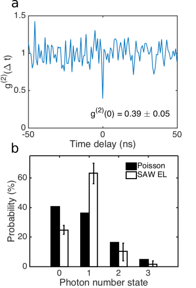
of the SAW-driven EL is obtained by finding the real contribution from each peak in the autocorrelation histogram (see Supplementary Information S5). The result is shown in Fig. 4(a). The suppressed photon-antibunching peak at gives , showing that the SAW-driven n-i-p junction can indeed produce single-photon emission. In addition, since the average number of electrons, , in a SAW minimum is 0.89, the probability distribution of photon-number states can be estimated. The wave function of electrons in a SAW minimum can be expressed in the Fock basis
| (1) |
where and denote the electron-number states and their respective probabilities. is thus a function of the probability distribution {}. When electrons (electron-number state ) arrive at the hole region, each of these electrons may recombine with a hole and produce a photon according to the internal quantum efficiency . Hence, up to photons will be produced from . These photons will then cause coincidences in an autocorrelation histogram. As a result, is also a function of the probability distribution {}. Assuming that has no projection to with (meaning that a SAW minimum can carry only up to three electrons) and given that and , a probability distribution {} of electron-number states (and photon-number states) in the SAW-driven n-i-p junction can be estimated to be {} (see Supplementary Information, section S6). This probability distribution is shown in Fig. 4(b), along with the distribution expected for a classical Poissonian light source (with the same average number ) for comparison. It can be seen that, in the SAW-driven n-i-p junction, the single-photon probability is greatly enhanced compared with the classical case. Based on this estimated probability distribution, when a detector receives a light signal from this SAW-driven n-i-p junction, the signal has a probability of – to actually be a single photon.
Although photon antibunching and single-photon emission have been experimentally demonstrated in this SAW-driven single-photon source, many improvements need to be done in future devices. In order to understand how to enhance , we build a simplified SAW-transport model to calculate the probability distribution of SAW-driven electrons. The result indicates that a more well-defined single-electron state (and thus higher ) may be achieved with a stronger confinement in the 1D channel and the SAW potential (see Supplementary Information S7). This may be done by using a narrower channel, and depositing ZnO thin film to enhance the SAW potential (Pedros2011, ). As for the low efficiency , this can be improved by surface passivation to reduce non-radiative surface states (Shiozaki2005, ), and by better capturing of the SAW-driven electrons and building an optical cavity (see Supplementary Information S8). On the other hand, to be useful for a quantum repeater or for quantum computing, good photon indistinguishability is important. The SAW-driven EL shows a peak with FWHM meV, which is two orders of magnitude larger than the spectral FWHM from a self-assembled QD, but comparable to the FWHM of single photons in photonic quantum networks (Tanida2012, ; Crespi2013, ; Spring2013, ; Wang2017, ; Sparrow2018, ). It has been shown experimentally that single photons with a FWHM meV can show good photon indistinguishability within a coherence time of 0.5-1 ps (coherent length m) and thus can be used to perform boson sampling and quantum simulation on integrated photonic chips. Hence, multiple SAW-driven single-photon sources may be integrated into a GaAs-based photonic waveguide chip (FattahPoor2013, ; Prtljaga2014, ; Jons2015, ), to achieve electrically-driven photonic quantum computation. Moreover, the photon indistinguishability in our device may be improved by using a high-quality quantum-well wafer with improved interface roughness (see Supplementary Information S8).
In this work, we have shown that a single-photon source can be made from a SAW-driven lateral n-i-p junction fabricated in a deterministic lithographic process using gates, etching and an interdigitated transducer. Hence, multiple single-photon sources at the same energy (limited by interface roughness) could be made in any arbitrary arrangement, which is beneficial for realising on-chip integrated photonic networks. On the other hand, since growing quantum wells with highly precise thickness is possible using molecular-beam epitaxy (MBE), and the single-photon energy in this device depends on the quantum-well thickness, making identical single-photon sources using this scheme is arguably easier than using self-assembled quantum dots. This is useful for applications that require photon entanglement. Finally, this device structure may also be fabricated using emerging 2D materials like WSe2 and MoS2 to realise more advanced quantum photon emitters (Mak2012, ; Zhang2014a, ). In these 2D materials, photon polarisations are coupled to the K and K’ valleys in their band structures owing to the breaking of inversion symmetry. Because the junction direction and the SAW direction can both be easily reversed in such a device structure, a chiral-single-photon source with electrically-controlled polarisation may be achieved using a similar device design, which will be useful in various quantum information technologies.
I Methods
I.1 Device Fabrication
The SAW-driven lateral n-i-p junction was made in a 15 nm undoped GaAs quantum well. The quantum-well layer structure consists of (from the top) a 10 nm GaAs capping layer, a 100 nm Al0.33Ga0.67As top barrier, a 15 nm GaAs quantum well, a 285 nm Al0.33Ga0.67As back barrier, and finally a 1 m GaAs buffer layer. n-type and p-type ohmic contacts were in direct contact with the quantum well. AuGeNi (for n-type contacts) and AuBe (for p-type contacts) were evaporated in regions recessed to the quantum well, and annealed at and respectively. Bridging gates for inducing electrons and holes from the ohmic contacts were fabricated by evaporating Ti/Au on a 100 nm Al2O3 insulator, which is on top of the ohmic contacts. Surface gates for extending charge carriers and forming a lateral n-i-p junction were fabricated on the wafer surface using electron-beam lithography. 1.2 m-wide 1D channel between the electron and hole regions was made by removing quantum well next to the 1D channel using electron-beam-defined wet etching. The interdigitated transducers with a period of 2.5 m were made using electron-beam lithography. The completed device was then mounted on a custom-made sample holder for measurement at 1.5 K.
I.2 Optical Setup
A EL signal emitted from a 2 m2 area is collected by a home-made confocal fibre-coupled lens assembly, the position of which is controlled by a three-axis piezoelectric stage relative to the sample. The EL signal is then sent through a single-mode fibre to optical components outside the cryostat. The EL signal was spectrally filtered by a 750mm Czerny-Turner spectrometer before being detected by a chilled EMCCD camera.
I.3 Time-resolved EL Measurement
A time-resolved EL setup consists of a SPAD, an arbitrary waveform generator that produces timing pulses, a time-to-digital converter, and a RF source that is synchronised to the timing pulses. The SPAD can be triggered by the detection of a single photon and will then output a signal pulse with a 40 ps jitter. The pulse generator also produces timing pulses with a 10 ps jitter. The signal pulses and the timing pulses are connected to the time-to-digital converter, which measures the time difference between a timing pulse and a signal pulse. The RF source is synchronised with the pulse generator by using a 10 MHz sync signal. The RF signal is used to generate a SAW signal synchronised to the timing pulses. A time-correlated histogram of a SAW-driven EL signal can thus be obtained by recording the time difference between timing pulses and SPAD signal pulses.
I.4 Hanbury Brown-Twiss Setup
An HBT setup consists of a 50:50 fibre-coupled beam-splitter and two SPADs. The beam-splitter splits the stream of photons in a SAW-driven EL signal into two beams. Each beam is sent to a SPAD. These two SPADs produce signal pulses when they are triggered by the incoming photons. In a start-stop autocorrelation method, a signal pulse from SPAD 1 (start) will cause the time-to-digital converter to begin time counting until the counter receives a signal pulse from SPAD 2 (stop). The counter then records one coincidence at the time delay between these two signal pulses. The two beams of photons will give rise to the autocorrelation histogram, which is the number of coincidences as a function of time delay.
References
- (1) Senellart, P., Solomon, G. & White, A. High-performance semiconductor quantum-dot single-photon sources. Nature Nanotechnology 12, 1026–1039 (2017).
- (2) Aharonovich, I., Englund, D. & Toth, M. Solid-state single-photon emitters. Nature Photonics 10, 631–641 (2016).
- (3) Shields, A. J. Semiconductor quantum light sources. Nature Photonics 1, 215–223 (2007).
- (4) Gisin, N., Ribordy, G., Tittel, W. & Zbinden, H. Quantum cryptography. Reviews of Modern Physics 74, 145–195 (2002).
- (5) Ekert, A. K. Quantum cryptography based on Bellâs theorem. Physical Review Letters 67, 661–663 (1991).
- (6) Lo, H. K. & Chau, H. F. Unconditional security of quantum key distribution over arbitrarily long distances. Science 283, 2050–2056 (1999).
- (7) Kimble, H. J. The quantum internet. Nature 453, 1023–1030 (2008).
- (8) Pirandola, S., Eisert, J., Weedbrook, C., Furusawa, A. & Braunstein, S. L. Advances in quantum teleportation. Nature Photonics 9, 641–652 (2015).
- (9) Horodecki, R., Horodecki, P., Horodecki, M. & Horodecki, K. Quantum entanglement. Reviews of Modern Physics 81, 865–942 (2009).
- (10) Giovannetti, V., Lloyd, S. & Maccone, L. Quantum-enhanced measurements: Beating the standard quantum limit. Science 306, 1330–1336 (2004).
- (11) Giovannetti, V., Lloyd, S. & MacCone, L. Advances in quantum metrology. Nature Photonics 5, 222–229 (2011).
- (12) Knill, E., Laflamme, R. & Milburn, G. J. A scheme for efficient quantum computation with linear optics. Nature 409, 46–52 (2001).
- (13) Kok, P. et al. Linear optical quantum computing with photonic qubits. Reviews of Modern Physics 79, 135–174 (2007).
- (14) He, Y. M. et al. On-demand semiconductor single-photon source with near-unity indistinguishability. Nature Nanotechnology 8, 213–217 (2013).
- (15) Somaschi, N. et al. Near-optimal single-photon sources in the solid state. Nature Photonics 10, 340–345 (2016).
- (16) Ding, X. et al. On-Demand Single Photons with High Extraction Efficiency and Near-Unity Indistinguishability from a Resonantly Driven Quantum Dot in a Micropillar. Physical Review Letters 116, 0202401 (2016).
- (17) Politi, A., Matthews, J. C. F. & O’Brien, J. L. Shor’s quantum factoring algorithm on a photonic chip. Science 325, 1221 (2009).
- (18) Crespi, A. et al. Integrated photonic quantum gates for polarization qubits. Nature Communications 2 (2011).
- (19) Harris, N. C. et al. Quantum transport simulations in a programmable nanophotonic processor. Nature Photonics 11, 447–452 (2017).
- (20) Qiang, X. et al. Large-scale silicon quantum photonics implementing arbitrary two-qubit processing. Nature Photonics 12, 534–539 (2018).
- (21) Spring, J. B. et al. Boson sampling on a photonic chip. Science 339, 798–801 (2013).
- (22) Wang, J. et al. Experimental quantum Hamiltonian learning. Nature Physics 13, 551–555 (2017).
- (23) Sparrow, C. et al. Simulating the vibrational quantum dynamics of molecules using photonics. Nature 557, 660–667 (2018).
- (24) Arrazola, J. M., Diamanti, E. & Kerenidis, I. Quantum superiority for verifying NP-complete problems with linear optics. npj Quantum Information 4, 56 (2018).
- (25) Kaltenbaek, R., Prevedel, R., Aspelmeyer, M. & Zeilinger, A. High-fidelity entanglement swapping with fully independent sources. Physical Review A - Atomic, Molecular, and Optical Physics 79, 040302 (2009).
- (26) Muller, A. et al. Resonance fluorescence from a coherently driven semiconductor quantum dot in a cavity. Physical Review Letters 99, 187402 (2007).
- (27) Ates, S. et al. Post-Selected Indistinguishable Photons from the Resonance Fluorescence. Physical Review Letters 103, 167402 (2009).
- (28) Migdall, A. L., Branning, D. & Castelletto, S. Tailoring single-photon and multiphoton probabilities of a single-photon on-demand source. Physical Review A - Atomic, Molecular, and Optical Physics 66, 4 (2002).
- (29) Collins, M. J. et al. Integrated spatial multiplexing of heralded single-photon sources. Nature Communications 4 (2013).
- (30) Giblin, S. P. et al. Towards a quantum representation of the ampere using single electron pumps. Nature Communications 3, 930 (2012).
- (31) Dubois, J. et al. Minimal-excitation states for electron quantum optics using levitons. Nature 502, 659 (2013).
- (32) Shilton, J. M. et al. High-frequency single-electron transport in a quasi-one-dimensional GaAs channel induced by surface acoustic waves. Journal of Physics Condensed Matter 8, L531–L539 (1996).
- (33) Talyanskii, V. I. et al. Single-electron transport in a one-dimensional channel by high-frequency surface acoustic waves. Phys. Rev. B 56, 15180–15184 (1997).
- (34) Ford, C. J. B. Transporting and manipulating single electrons in surface-acoustic-wave minima. Physica Status Solidi (B) Basic Research 254, 1600658 (2017).
- (35) Bäuerle, C. et al. Coherent control of single electrons: a review of current progress. Reports on Progress in Physics 81, 056503 (2018).
- (36) Foden, C. L., Talyanskii, V. I., Milburn, G. J., Leadbeater, M. L. & Pepper, M. High-frequency acousto-electric single-photon source. Physical Review A 62, 011803 (2000).
- (37) Hosey, T. et al. Lateral n-p junction for acoustoelectric nanocircuits. Applied Physics Letters 85, 491–493 (2004).
- (38) Cecchini, M. et al. Surface acoustic wave-induced electroluminescence intensity oscillation in planar light-emitting devices. Applied Physics Letters 86, 1–3 (2005).
- (39) Smith, S. J. et al. Lateral light emitting n-i-p diodes in InSbAl[sub x]In[sub 1x]Sb quantum wells. Applied Physics Letters 89, 111118 (2006).
- (40) Gell, J. R. et al. Surface-acoustic-wave-driven luminescence from a lateral p-n junction. Applied Physics Letters 89, 243505 (2006).
- (41) De Simoni, G., Piazza, V., Sorba, L., Biasiol, G. & Beltram, F. Acoustoelectric luminescence from a field-effect n-i-p lateral junction. Applied Physics Letters 94, 121103 (2009).
- (42) Dai, V.-T. et al. High-quality planar light emitting diode formed by induced two-dimensional electron and hole gases. Optics express 22, 3811–7 (2014).
- (43) Couto, O. D. D. et al. Photon anti-bunching in acoustically pumped quantum dots. Nature Photonics 3, 645–648 (2009).
- (44) Weiß, M. et al. Surface acoustic wave regulated single photon emission from a coupled quantum dot-nanocavity system. Applied Physics Letters 109, 033105 (2016).
- (45) Villa, B. et al. Surface acoustic wave modulation of a coherently driven quantum dot in a pillar microcavity. Applied Physics Letters 111, 011103 (2017).
- (46) Demichel, O., Heiss, M., Bleuse, J., Mariette, H. & Fontcuberta Morral, I. A. Impact of surfaces on the optical properties of GaAs nanowires. Applied Physics Letters 97, 201907 (2010).
- (47) Shiozaki, N., Anantathanasarn, S., Sato, T., Hashizume, T. & Hasegawa, H. Surface-related reduction of photoluminescence in GaAs quantum wires and its recovery by new passivation. Applied Surface Science 244, 71–74 (2005).
- (48) Hegarty, J. & Sturge, M. D. Studies of exciton localization in quantum-well structures by nonlinear-optical techniques. Journal of the Optical Society of America B 2, 1143 (1985).
- (49) Srinivas, V., Hryniewicz, J., Chen, Y. J. & Wood, C. E. Intrinsic linewidths and radiative lifetimes of free excitons in GaAs quantum wells. Physical Review B 46, 10193–10196 (1992).
- (50) Singh, J. Electronic and optoelectronic properties of semiconductor structures (Cambridge University Press, 2003), 1 edn.
- (51) Ziarkash, A. W., Joshi, S. K., Stipčević, M. & Ursin, R. Comparative study of afterpulsing behavior and models in single photon counting avalanche photo diode detectors. Scientific Reports 8 (2018).
- (52) Feldmann, J. et al. Linewidth dependence of radiative exciton lifetimes in quantum wells. Physical Review Letters 59, 2337–2340 (1987).
- (53) Angeloni, L. et al. Time-resolved photoluminescence of GaAs/GaAlAs M.Q.W. structures under picosecond excitation. Superlattices and Microstructures 5, 549–554 (1989).
- (54) Pedros, J. et al. Guided propagation of surface acoustic waves and piezoelectric field enhancement in ZnO/GaAs systems. Journal of Applied Physics 110, 103501 (2011).
- (55) Tanida, M., Okamoto, R. & Takeuchi, S. Highly indistinguishable heralded single-photon sources using parametric down conversion. Optics Express 20, 15275–15285 (2012).
- (56) Crespi, A. et al. Integrated multimode interferometers with arbitrary designs for photonic boson sampling. Nature Photonics 7, 545–549 (2013).
- (57) Fattah Poor, S. et al. Efficient coupling of single photons to ridge-waveguide photonic integrated circuits. Applied Physics Letters 102, 131105 (2013).
- (58) Prtljaga, N. et al. Monolithic integration of a quantum emitter with a compact on-chip beam-splitter. Applied Physics Letters 104, 231107 (2014).
- (59) Jöns, K. D. et al. Monolithic on-chip integration of semiconductor waveguides, beamsplitters and single-photon sources. Journal of Physics D: Applied Physics 48, 085101 (2015).
- (60) Mak, K. F., He, K., Shan, J. & Heinz, T. F. Control of valley polarization in monolayer MoS2by optical helicity. Nature Nanotechnology 7, 494–498 (2012).
- (61) Zhang, Y. J., Oka, T., Suzuki, R., Ye, J. T. & Iwasa, Y. Electrically Switchable Chiral Light-Emitting Transistor. Science 344, 725 – 728 (2014).
Acknowledgements This work was supported by the European Union Horizon 2020 research and innovation program under Marie Skłodowska-Curie Grant Agreement No. 642688 (SAWtrain), and the UK EPSRC [Grant Nos. EP/J003417/1 and EP/H017720/1]. A.N. was supported by the UK Department for Business, Innovation and Skills. TKH was supported by the Cambridge Overseas Trust. JP acknowledges the support from the Spanish MICINN (Programa Nacional de Movilidad de Recursos Humanos I+D+i) and from the 7th European Community Framework Programme (Marie Curie Intra-European Fellowship, Project no. 235515) during his time at the University of Cambridge, as well as from the Spanish MINECO (grant RyC-2015-18968) now at Universidad Politécnica de Madrid. We thank Mete Atatüre for the loan of the SPADs and the time-to-digital converter and Charles Smith and Joanna Waldie for the loan of the arbitrary waveform generator. We also thank Peter Spencer for assistance with the optical setup.
Author contributions Project planning: CJBF, TKH and JP; MBE growth: IF and DAR; E-beam lithography: JPG and TAM; sample design and fabrication: TKH, YC, AR, SKS and AN; electrostatic calculation: HH; scanning cryogenic microscope: JP, YC, RTP, TKH, SKS, HH and CJBF; Spectrometer, HBT and time-resolved setup: AN, GÉM, MJS and RTP; transport and optical measurements: TKH, AN and AR; analysis of results and theoretical interpretation: TKH and CJBF.
Data availability Data associated with this work are available at the University of Cambridge data repository (https://doi.org/???; see ref. ??).
Competing Interests The authors declare that they have no competing financial interests.
Correspondence Correspondence and requests for materials should be addressed to C. J. B. Ford (email: cjbf@cam.ac.uk) or Tzu-Kan Hsiao (email: tzu-kan.hsiao@cantab.net or tkh28@cam.ac.uk).