Reduced Thermal Conductivity of Epitaxial GaAs on Si due to Symmetry-breaking Biaxial Strain
Abstract
Epitaxial growth of III-V semiconductors on Si is a promising route for silicon photonics. Threading dislocations and the residual thermal stress generated during growth are expected to affect the thermal conductivity of the III-V semiconductors, which is crucial for efficient heat dissipation from photonic devices built on this platform. In this work, we combine a non-contact laser-induced transient thermal grating technique with ab initio phonon simulations to investigate the in-plane thermal transport of epitaxial GaAs-based buffer layers on Si, employed in the fabrication of III-V quantum dot lasers. Surprisingly, we find a significant reduction of the in-plane thermal conductivity of GaAs, up to 19, as a result of a small in-plane biaxial stress of 250 MPa. Using ab initio phonon calculations, we attribute this effect to the enhancement of phonon-phonon scattering caused by the in-plane biaxial stress, which breaks the cubic crystal symmetry of GaAs. Our results indicate the importance of eliminating the residual thermal stress in the epitaxial III-V layers on Si to avoid the reduction of thermal conductivity and facilitate heat dissipation. Additionally, our results showcase potential means of effectively controlling thermal conductivity of solids with external strain/stress.
I Introduction
The field of photonic integrated circuits is rapidly becoming an important contender in the development of optoelectronic devices with improved performance for diverse applications such as high-speed telecommunications and information processing Thomson et al. (2016); Liu and Bowers (2018). Among the available integration strategies and material platforms, direct epitaxial growth of III-V compound semiconductors such as GaAs and InP on Si for the fabrication of photonic devices has emerged as a promising direction owing to the reduced cost, the better heat-dissipation capability, the larger available device area and the prospect for scalable manufacturingLiu and Bowers (2018); Sakai and Wada (1994); Wang et al. (2011). However, the epitaxial growth process of III-V materials on Si has its own share of obstacles, mainly caused by the lattice constant mismatch, the formation of anti-phase domains (APD) (due to polarity mismatchKroemer et al. (1980)) and the thermal expansion mismatchSakai and Wada (1994). The resulting high threading dislocation density (TDD) and residual thermal stress in the III-V layer are the major factors that negatively impact the efficiency, stability and lifetime of the photonic devicesSakai and Wada (1994); Liu et al. (2015). Various methods have been developed in order to tackle these problems Liu and Bowers (2018). Recently, the combination of a thin GaP(45 nm) buffer layer grown on (001) Si substrates (for suppression of APD formation) with buffer structures comprised of GaAs and strained superlattices as dislocation filters has led to the fabrication of high efficiency, long lifetime and low threshold III-V quantum dot lasers Jung et al. (2018a, b) on Si. In these state-of-the-art devices, the TDD is typically reduced to the level of , and the residual thermal stress due to the mismatch in the thermal expansion coefficients of GaAs and Si is MPa, corresponding to a strain of roughly 0.16%Jung et al. (2017); Sugo et al. (1989).
Temperature effects also play an important role in the performance and the lifetime of integrated photonic devices, as an elevated temperature can facilitate the motion and the growth of dislocations, which consequently can lead to device aging and operational malfunction Sakai and Wada (1994); Thomson et al. (2016). In this light, efficient heat dissipation from the III-V materials grown on Si is desirable. In principle, both the presence of threading dislocationsZou et al. (2002); Mion et al. (2006) and the residual thermal stressBorca-Tasciuc et al. (2000); Li et al. (2010); Parrish et al. (2014); Alam et al. (2015) can affect the thermal conductivity of the epitaxial III-V semiconductors grown on Si, directly impacting the thermal management in devices with multilayered structures. Despite a sparse number of previous studies regarding thermal transport in GaAs based devicesNadri et al. (2018), there has not been direct experimental evaluation of the effect of the TDD and the residual thermal stress on the thermal conductivity of realistic III-V materials grown on Si for photonic integrated circuit applications.
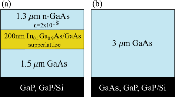
In this study, we present in-plane thermal transport measurements of 3 m thick GaAs based buffer layers employed in the fabrication of III-V quantum dot lasers. The measurements were performed using an optical non-contact, non-destructive method known as laser-induced transient thermal grating (TTG) Eichler et al. (1986); Rogers and Maznev (2000). We analyzed two multilayered samples with the GaAs based buffer layers and the /GaAs strained superlattice dislocation filter layers epitaxially grown on different substrates: one on a GaP substrate, and the other on a GaP/Si template (45 nm of GaP on a (001) Si substrate), as shown in Fig. 1(a). Both structures are fundamentally the same; their only difference is the formation of an in-plane residual tensile stress of 250 MPa resulting from the growing process (described in section II) on the GaP/Si substrate Jung et al. (2018a). The stressed buffer layer showed a decrease of 13 in thermal conductivity compared to the unstressed layer. In order to confirm the effect of the residual thermal stress, we further performed TTG measurements on 3 m thick GaAs films epitaxially grown on GaAs, GaP and GaP/Si substrates (Fig. 1(b)), and verified a reduction of the in-plane thermal conductivity. To understand the results, we conducted ab initio phonon calculations based on density functional theory (DFT), which predicts a 21 reduction in the in-plane thermal conductivity of GaAs under a symmetry-breaking 250 MPa biaxial tesile strain, in good agreement with the experimental results.
II Sample preparation
Detailed description of the growth process can be found elsewhereJung et al. (2017); Volz et al. (2011); Huang et al. (2014, 2018), and a brief overview is given here. Two different substrates were selected for growth, GaP, and GaP/Si (see Fig. 1), hereafter referred to as samples s-GaP and s-Si, respectively. The GaP/Si template was provided by GmbH and consisted of a 775 m thick (001) on-axis p-doped Si substrate with a 200 nm thick n-doped Si homo-epitaxial buffer and a subsequent 45 nm thick n-doped GaP nucleation layer deposited by metal-organic chemical vapor depositionVolz et al. (2011). A 1.5 m GaAs layer was then grown on both substrates in a solid-source molecular beam epitaxy (MBE), as previously reportedHuang et al. (2014); Jung et al. (2017). A thermal annealing cycle was employed after the growth to facilitate dislocation annihilation Huang et al. (2014); Jung et al. (2017). Following this step, a 200 nm /GaAs strained superlattice layer was grown. This layer is used as dislocation filters for successive film growths Volz et al. (2011); Huang et al. (2014, 2018). Finally, 1.3 m of GaAs (doped ) was grown, providing a template for further III-V device fabrication. The TDD of cm-2 and cm-2 were measured for the top GaAs buffer layer in samples s-GaP and s-Si, respectively, using electron channeling contrast imaging (ECCI) techniqueJung et al. (2018a). There is an additional in-plane biaxial residual thermal stress of 250 MPa in sample s-Si due to the mismatch of the thermal expansion coefficients of GaAs and Si. This residual stress is absent in sample s-GaP because of the matching thermal expansion coefficients of GaAs and GaP. The residual thermal stress was determined by measuring the red shift of the photoluminescence peak of the GaAs layersJung et al. (2017); Sugo et al. (1989). In addition to samples s-GaP and s-Si, a set of three GaAs films of 3 m thickness were grown on GaAs, GaP and GaP/Si (see Fig. 1(b)) substrates using MBE under the same growth conditions as s-GaP and s-Si. The GaAs film grown on GaP/Si also shows the in-plane residual tensile stress of 250 MPa.
III Thermal transport measurements and calculations
III.1 Experimental methodology
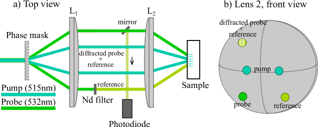
In-plane thermal transport was measured using the laser-induced TTG technique. Figure 2 shows a schematic of our TTG setup that includes a heterodyne detection scheme. For extensive details regarding heterodyne in a TTG experiment, we refer the readers to the references Maznev et al. (1998); Vega-Flick et al. (2015). Briefly, a transmission optical diffraction grating (also known as a phase mask) is used to split the excitation and the probe beams into two pairs. A two lens confocal imaging system is used to recombine the excitation and probe beams onto the sample (the focal lengths were cm and cm, respectively). The excitation pulses (pump beams) are from a femtosecond Yb-doped fiber laser at 1030 nm (Clark-MXR IMPULSE), have 260 fs pulse width, 250 kHz repetition rate and are frequency doubled to 515 nm wavelength. The spot diameter at the sample is 100 m with a nJ pulse energy. The probe beam is a CW laser with a 532 nm wavelength, 90 m spot diameter and mW power. The two excitation laser pulses are crossed at an angle 2 in order to produce an intensity pattern with a periodicity , where is the optical wavelength. In the case of optically opaque samples, absorption of the laser light creates a spatially periodic temperature profile at the surface, which will remain until the thermal energy is redistributed from peak to null. The time dependence of the temperature profile can be monitored by diffracting a probe CW laser off of the heated region. One of the probe beams is attenuated and used as the local oscillator (reference). Overlapping the reference and the diffracted probe light leads to amplification and linearization of the observed signal (heterodyne detection) Goodno et al. (1998); Maznev et al. (1998), and is subsequently monitored using a fast photodiode (Hamamatsu C5658) connected to an oscilloscope (Tektronix TDS784A). The diffraction of the probe beam is due to both surface displacement induced by thermal expansion and changes in the reflectivity with respect to periodic temperature profile Johnson et al. (2012); Käding et al. (1995).
By quantitatively analyzing the time dependence of the TTG signal, we can obtain the in-plane thermal diffusivity of the sample, which is the material property that physically determines the speed of heat propagation due to temperature differences and is related to the thermal conductivity through the expression , where is the density, is heat capacity and is the thermal diffusivity. A unique feature of the TTG technique is that the length scale of the spatial heating profile can be conveniently controlled by changing the period of the induced thermal grating, which in turn changes the thermal penetration depth probed by TTG.
The multilayered samples measured in this work were considered as a single film with “effective” thermal properties, grown on a semi-infinite substrate. In this case, the time evolution of the TTG signal can be modeled by solving both the thermal diffusion and thermo-elastic equations with a periodic spatial heating source, as presented in reference Käding et al. (1995). In the case where in-plane thermal transport is dominated by the film, the solution for the TTG signal simplifies to that of a semi-infinite half-space with a thermal diffusivity , and is given by the expression Johnson et al. (2012); Käding et al. (1995)
| (1) |
where is the complementary error function, is the TTG wavevector, is the TTG period, and are fitting parameters. Equation 1 assumes that the thermoreflectance contribution to the TTG signal is small compared to the surface displacement, which is generally the case for non-metalsKäding et al. (1995).
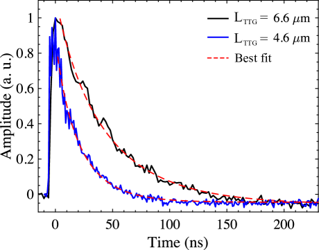
Figure 3 shows typical time traces obtained for sample s-Si using of 6.6 m and 4.6 m. The dashed lines correspond to the best fits using Eq. 1. As the time scale probed here was tens to hundreds of nanoseconds, the fast dynamics induced by photocarriers, typically happening on the sub-nanosecond time scale, has no effect on the results.
III.2 Thermal conductivity calculations
In order to elucidate the effect that the residual thermal stress has on thermal transport, we also performed ab initio thermal conductivity calculations of GaAs with or without the in-plane biaxial strain. Under the Boltzmann transport equation (BTE) formalism Turney et al. (2009), the thermal conductivity can be expressed as
| (2) |
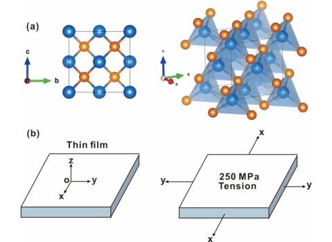
where and are the phonon wavevector and phonon branch, respectively, is the mode-specific heat capacity, is the group velocity, and is the phonon lifetime. We applied density functional perturbation theory (DFPT) Baroni et al. (2001) in order to determine the lattice dynamics and consequently calculate the thermal conductivity for stressed and un-stressed GaAs. The technical details regarding the ab initio calculations are shown in Appendix A. Briefly, using the DFPT method we calculated the harmonic second-order interatomic force constants (IFCs), which we employed to determine the phonon dispersion across the whole Brillouin zone (BZ). From here, the group velocity and the heat capacity were calculated as and (where is the mode specific phonon frequency, is the reduced Planck’s constant, is the Bose-Einstein distribution and is the temperature). In the following step, we employed the supercell frozen-phonon approach Esfarjani et al. (2011) in order to calculate the third-order (anharmonic) IFCs. In conjunction with the Fermi’s golden rule, the anharmonic IFCs were used to calculate the phonon lifetime . All calculations used a conventional cell, which included 8 atoms (see Fig. 4(a)).
We calculated the thermal conductivity of GaAs under two different cases of residual stress: i) 0 Pa (unstressed GaAs) and ii) 250 MPa in-plane biaxial stress (X-Y plane, see Fig. 4(b)). As a control, we also calculated the thermal conductivity of GaAs under an isotropic stress of 250 MPa along all three directions. In the calculation, the isotropic stress was implemented by uniformly scaling the conventional cell until the desirable stress was obtained; the biaxial stress was implemented by uniformly adjusting the lattice constants along the X and Y directions, while relaxing the atom positions in the conventional cell and the lattice constant along the Z direction, until the desired in-plane biaxial stress and zero cross-plane stress were achieved. The optimized structure under stress corresponds to a biaxial strain of 0.15%, in good agreement with experimental measurementsSakai and Wada (1994); Jung et al. (2017); Sugo et al. (1989).
IV Results and discussion
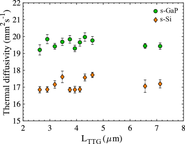
Figure 5 (a) shows the measured thermal diffusivity values for the s-GaP and s-Si buffer layer samples as a function of the TTG period () using Eq. 1. The obtained values are independent of , indicating the absence of a substrate effect, i.e. the multilayered structure dominates the in-plane thermal transport, therefore we are effectively measuring the multilayered structures as a bulk semi-infinite material. There is a significant decrease in the in-plane thermal diffusivity of the multilayer structure when it is grown on the GaP/Si substrate ( lower thermal diffusivity). Given the identical structures and similar TDD of the two samples, we attribute the difference in thermal diffusivity to the in-plane residual stress in the sample s-Si. This significant reduction of thermal diffusivity is unexpected given the small magnitude of the stress (0.16% strain).
| Sample | D(mm2/s) | (W/mK) |
|---|---|---|
| s-GaP | 19.60.25 | - |
| s-Si | 17.10.3 | - |
| GaP | 33.31 | 54.61.6 |
| Si | 59.30.8 | 105.51.4 |
| GaP/Si11145 nm of GaP grown on Si. The same heat capacity and density of Si was considered for the estimation of . | 56.71.5 | 100.9.2.7 |
| GaAs | 23.50.3 | 41.30.5 |
| GaAs(3m)/GaAs | 18.7 0.62 | 32.91.1 |
| GaAs(3m)/GaP | 18.5 0.63 | 32.61.1 |
| GaAs(3m)/GaP(45nm)/Si | 15.2 0.56 | 26.71.0 |
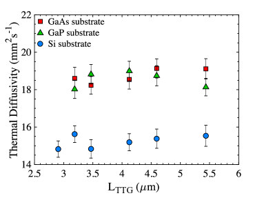
In order to experimentally corroborate the residual stress as the main factor in the reduction of the thermal diffusivity, we measured GaAs films of 3 m thickness epitaxially grown on GaAs, GaP and GaP/Si (45 nm of GaP on Si) substrates, as well as the substrates themselves (all obtained values are shown in Table 1). The TTG time traces were normalized and analyzed using the complete solution to the thermo-elastic equation Käding et al. (1995) and only the thermal diffusivity of the GaAs film was used as a fitting parameter. All other material properties were taken from literature (see Appendix B). 222The fitting procedure using the complete solution to the thermo-elastic equations was performed with and without the consideration of a thermal boundary resistance between the GaAs film and the substrate. With a resistance value of mK/W, we found that the fitted thermal diffusivity values were affected by less than 0.5. The thermal boundary resistance was therefore considered negligible in the rest of the manuscript.
Figure 6 shows the obtained thermal diffusivities as a function of . The GaAs film shows similar values for the case of GaP and GaAs substrates ( 18.6 mm2s-1,see Table 1). This is expected given that the film is not under residual stress when using GaAs or GaP substrates due to the thermal expansion coefficients of GaAs and GaP being similar Roesener et al. (2013). Comparing these results to the values obtained using GaAs grown on the GaP/Si substrate (15.2 mm2s-1), we found a reduction of 19 in the thermal diffusivity of the stressed film grown on GaP/Si. Additionally, the unstressed film has a lower thermal diffusivity compared to the bulk value ( reduction). This can be explained using the Fuchs-Sondheimer theory for thin films, where the effective phonon mean free path (MFP) is reduced due to an increase in the boundary scattering of phonons at the film surfaces Sondheimer (1952); Chen (2005). We also note that the thermal diffusivity of the bare GaAs films (Fig. 1(b)) without the dislocation filter layers is consistently lower than that of the samples with the dislocation filter layers (Fig. 1(a)) grown on the same substrates, which can be attributed to the effect of the threading dislocations on phonon transport. It has been known that the threading dislocations can scatter phononsLi et al. (2018) and reduce the thermal conductivity, for example in GaNZou et al. (2002); Mion et al. (2006). A systematic study of the effect of TDD on thermal transport in epitaxial GaAs on Si will be reported in a separate publication.
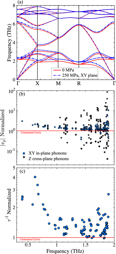
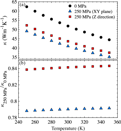
To compare our experimental findings with theory, we performed calculations of the in-plane thermal conductivity of stressed and unstressed GaAs following the procedure described in Section III B. The 250 MPa of tensile stress results in a 0.15% variation in the lattice constant. This changes the atomic positions in the conventional cell, leading to variations in the phonon band structure. Figure 7(a) shows the phonon dispersion relation comparison between 0 and 250 MPa tensile stress in the XY plane. The high-frequency optical phonon branches show very small changes due to the stress. Only small changes are visible in the direction. In contrast, the lower frequency acoustic branches show a consistent shift towards higher frequencies. Figure 7(b) and (c) shows normalized values (with respect to the unstressed film) of the heat carrying phonon group velocities and the phonon scattering rates, respectively (phonons with frequencies lower than 2 THz, which are the major heat carriers in GaAs). In the case of the group velocities, cross-plane phonons have a symmetric variation across the base line as a function of frequency, in contrast to in-plane phonons showing a small net increase in the group velocity as a function of frequency, which does not explain the reduced thermal conductivity of GaAs under stress. Strikingly, the small 0.15% biaxial strain significantly increases the scattering rates of low frequency acoustic phonons, up to a factor of 4, as shown in Fig. 7(c). This is expected to have an important impact on the thermal conductivity, as these low frequency acoustic phonons are the major heat carriers in GaAs. Figure 8(a) shows the calculated isotropic thermal conductivity of unstressed GaAs (circles), the calculated in-plane (triangles) and cross-plane (squares) thermal conductivity of GaAs under the biaxial stress of 250 MPa at different temperatures. The normalized in-plane and cross-plane thermal conductivity of the stressed GaAs with respect to the unstressed GaAs is plotted in Fig. 8(b). The thermal conductivity decreases by an average of and for in-plane and cross-plane directions, respectively. The reduction of the in-plane thermal conductivity is caused by the increased phonon scattering rates in the stressed GaAs, and the relative magnitude of the reduction is in good agreement with our experimental results.
The effect of stress/strain on the thermal conductivity of solids has been intensively studied beforePicu et al. (2003); Bhowmick and Shenoy (2006); Li et al. (2010); Parrish et al. (2014). The general finding is that tensile stress reduces the thermal conductivity of solids due to the reduction of phonon group velocities and/or specific heat. In previous studies, however, significant reduction of the thermal conductivity typically happens at much higher stress/strain. For example, Parrish et al.Parrish et al. (2014) predicted a 10% reduction of the thermal conductivity of Si under a tensile strain of 3%, corresponding to a tensile stress of 7 GPa. Li et al.Li et al. (2010) predicted similar values for bulk Si and diamond. A key difference here is that isotropic strain was applied in these previous studies, whereas in the present study GaAs is under an in-plane biaxial strain. Although isotropic strain modifies the effective “stiffness” of the material, the crystal structure of the material is uniformly scaled along all directions and the crystal symmetry is preserved (with the exception of pressure-driven phase transitionsHohensee et al. (2015); Yue et al. (2018)). In contrast, in-plane biaxial strain in GaAs also breaks its cubic crystal symmetry with increased lattice constants along the X and Y directions and decreased lattice constant along the Z direction. It is known that high crystal symmetry imposes selection rules on the scattering matrix elements and limits the possible channels of phonon scatteringInui et al. (2012). In particular, this symmetry-breaking strain effect on electron-phonon scattering in Si and III-V semiconductors has been studied and well understoodBaykan et al. (2010); Sjakste et al. (2013); Sun et al. (2007); Sjakste et al. (2006) and the same principle also applies to phonon-phonon scattering. To confirm that the observed significant reduction of thermal conductivity in this work originates from the symmetry-breaking biaxial strain, we also conducted ab initio thermal conductivity calculation of GaAs under an isotropic tensile stress of 250 MPa, where the reduction of thermal conductivity was found to be within 2%. A more rigorous analysis based on group theory is in progress and beyond the scope of this work.
Our findings have multiple implications. On one hand, the significant reduction of the thermal conductivity of epitaxial GaAs on Si due to the residual thermal stress is detrimental to the heat dissipation capability of photonic devices built on this platform. The residual thermal stress is already known to induce motion of the dislocationsSakai and Wada (1994); Jung et al. (2018a) and reduce the device lifetime, and our new findings provide additional motivation to address the residual thermal stress through rational design of device structures, e.g. by forming high aspect-ratio structures such as micro-ring lasersJung et al. (2018a). On the other hand, our results also provide a potential route to design solid-state thermal switchesWehmeyer et al. (2017), whose thermal conductivity can be effectively controlled by external strain/stress.
V Conclusions
In conclusion, we measured the in-plane thermal transport of epitaxial GaAs grown on Si, and discovered a reduction of the thermal diffusivity up to 19%. By comparing the measurement results of GaAs grown on different substrates, we clarified that the reduction of thermal diffusivity was due to the residual in-plane thermal stress. We further corroborated the result using ab initio phonon calculations, and attributed the reduction to enhanced phonon-phonon scattering due to the symmetry-breaking in-plane biaxial stress. Our results reaffirm the importance of addressing the residual thermal stress in epitaxial III-V materials on Si for photonic and electronic applications and may open up new venues towards controlling the thermal conductivity of bulk solids with external means. It will also be of interest to investigate the effect of the TDD and residual thermal stress on the dynamics of hot carriers using time-resolved imaging techniquesLiao and Najafi (2017), as well as dislocation-mediated anisotropic thermal transportSun et al. .
Acknowledgments
This work is based on research supported by the Academic Senate Faculty Research Grant from University of California, Santa Barbara (UCSB). B. L. acknowledges the support of a Regents’ Junior Faculty Fellowship from UCSB.
Appendix A: Theoretical calculation, technical details
The ab initio calculation was performed using the Vienna ab-initio simulation package (VASP)Kresse and Furthmüller (1996a, b) for the DFT and DFPT calculations. For all calculations, we adopted the Perdew-Burke-Ernzerhof (PBE) generalized gradient approximation (GGA)Perdew et al. (1996) as the exchange-correlation functional. We employed the pseudopotentials based on the projector augmented wave (PAW)Blöchl (1994); Kresse and Joubert (1999). The kinetic energy cutoff of plane-wave functions was set at and the tolerance for the energy convergence was . The Monkhorst-PackMonkhorst and Pack (1976) k-mesh of was used to sample the Brillouin zone. We checked the convergence for the cutoff energy of the plane wave basis and the k-grid density. We used conventional cell which includes 8 atoms in our simulations.
Details regarding the DFPT calculations of the lattice dynamics are as follows. The harmonic second-order IFC tensors were calculated using the PHONOPYTogo and Tanaka (2015). The non-analytical terms were added to dynamical matrices to capture the polar phonon effects with the Born charges (, ) and the dielectric constant () which were comparable to previous reportsLuo et al. (2013). Fine q-grid meshes () were adoped in the DFPT calculations to capture the long-range polar interactions in GaAs.
The third-order (anharmonic) IFCs were calculated using a supercell frozen-phonon approach. supercells were used for both calculations with or without the strain. The interatomic interactions were considered up to the 6th nearest neighbours, meaning that the cutoff radius was taken as . The thermal conductivity, , was obtained from solving the phonon Boltzmann transport equationTurney et al. (2009) iteratively as implemented in the ShengBTELi et al. (2014) package.
Appendix B: Material properties
Table 2 shows the literature values for the material properties used to analyze the TTG time traces. The thermal expansion coefficient, Poisson’s ratio, shear modulus, heat capacity, and density were employed in the calculations of the full solution to the thermo-elastic equations. In the case of the multilayer samples (shown in Fig. 1). the TTG data was easily analyzed using Eq. 1, where the only unknown parameter is the effective thermal diffusivity .
| GaAs | GaP | Si | |
| (K-1)333Thermal expansion coefficient | 5.710-6 | 2.610-6 | 4.710-6 |
| (GPa)444Shear modulus | 32.4 | 62 | 39.2 |
| 555Poisson’s ratio | 0.31 | 0.27 | 0.31 |
| (kgm-3)666Density | 5320 | 2329 | 4138 |
| (J/K) 777Heat capacity | 330 | 704 | 430 |
References
References
- Thomson et al. (2016) D. Thomson, A. Zilkie, J. E. Bowers, T. Komljenovic, G. T. Reed, L. Vivien, D. Marris-Morini, E. Cassan, L. Virot, J.-M. Fédéli, et al., Journal of Optics 18, 073003 (2016).
- Liu and Bowers (2018) A. Y. Liu and J. Bowers, IEEE Journal of Selected Topics in Quantum Electronics 24, 1 (2018).
- Sakai and Wada (1994) S. Sakai and N. Wada, Fiber and Integrated Optics 13, 31 (1994).
- Wang et al. (2011) T. Wang, H. Liu, A. Lee, F. Pozzi, and A. Seeds, Optics express 19, 11381 (2011).
- Kroemer et al. (1980) H. Kroemer, K. J. Polasko, and S. C. Wright, Applied Physics Letters 36, 763 (1980).
- Liu et al. (2015) A. Y. Liu, R. W. Herrick, O. Ueda, P. M. Petroff, A. C. Gossard, and J. E. Bowers, IEEE Journal of Selected Topics in Quantum Electronics 21, 1900708 (2015).
- Jung et al. (2018a) D. Jung, R. Herrick, J. Norman, K. Turnlund, C. Jan, K. Feng, A. C. Gossard, and J. E. Bowers, Applied Physics Letters 112, 153507 (2018a).
- Jung et al. (2018b) D. Jung, Z. Zhang, J. Norman, R. Herrick, M. Kennedy, P. Patel, K. Turnlund, C. Jan, Y. Wan, A. C. Gossard, et al., ACS Photonics 5, 1094 (2018b).
- Jung et al. (2017) D. Jung, P. G. Callahan, B. Shin, K. Mukherjee, A. C. Gossard, and J. E. Bowers, Journal of Applied Physics 122, 225703 (2017).
- Sugo et al. (1989) M. Sugo, N. Uchida, A. Yamamoto, and T. Nishioka, Journal of Applied Physics 65 (1989).
- Zou et al. (2002) J. Zou, D. Kotchetkov, A. Balandin, D. Florescu, and F. H. Pollak, Journal of applied physics 92, 2534 (2002).
- Mion et al. (2006) C. Mion, J. Muth, E. Preble, and D. Hanser, Applied Physics Letters 89, 092123 (2006).
- Borca-Tasciuc et al. (2000) T. Borca-Tasciuc, W. Liu, J. Liu, T. Zeng, D. W. Song, C. D. Moore, G. Chen, K. L. Wang, M. S. Goorsky, T. Radetic, et al., Superlattices and microstructures 28, 199 (2000).
- Li et al. (2010) X. Li, K. Maute, L. Dunn, and R. Yang, Physical Review B 81 (2010).
- Parrish et al. (2014) K. D. Parrish, A. Jain, J. M. Larkin, W. A. Saidi, and A. J. H. McGaughey, Physical Review B 90 (2014).
- Alam et al. (2015) M. T. Alam, R. A. Pulavarthy, C. Muratore, and M. A. Haque, Nanoscale and Microscale Thermophysical Engineering 19 (2015).
- Nadri et al. (2018) S. Nadri, N. D. Sauber, M. E. Cyberey, A. W. Lichtenberger, N. S. Barker, M. Zebarjadi, and R. M. Weikle, IEEE Transactions on Electron Devices (2018).
- Eichler et al. (1986) H. J. Eichler, P. Gunter, and D. Pohl, Laser-Induced Dynamic Gratings, edited by Springer-Verlag (Berlin, 1986).
- Rogers and Maznev (2000) J. A. Rogers and A. A. Maznev, Annu. Rev. Mater. Sci. 30, 117 (2000).
- Volz et al. (2011) K. Volz, A. Beyer, W. Witte, J. Ohlmann, I. Nemeth, B. Kunert, and W. Stolz, Journal of Crystal Growth 315 (2011).
- Huang et al. (2014) X. Huang, Y. Song, T. Masuda, D. Jung, and M. Lee, Electronics Letters 50, 1226 (2014).
- Huang et al. (2018) H. Huang, J. Duan, D. Jung, A. Y. Liu, Z. Zhang, J. Norman, J. E. Bowers, and F. Grillot, Optical Society of America 35 (2018).
- Maznev et al. (1998) A. A. Maznev, K. A. Nelson, and J. A. Rogers, Opt. Lett. 23, 1319 (1998).
- Vega-Flick et al. (2015) A. Vega-Flick, J. K. Eliason, A. A. Maznev, A. Khanolkar, M. A. Abi Ghanem, N. Boechler, J. J. Alvarado-Gil, and K. A. Nelson, Rev. Sci. Instrum. 86, 123101 (2015).
- Goodno et al. (1998) G. D. Goodno, G. Dadusc, and R. J. Miller, J. Opt. Soc. Am. B: Opt. Phys. 15, 1791 (1998).
- Johnson et al. (2012) J. A. Johnson, A. A. Maznev, M. T. Bulsara, E. A. Fitzgerald, T. C. Harman, S. Calawa, C. J. Vineis, G. Turner, and K. A. Nelson, J. App. Phys. 111, 023503 (2012).
- Käding et al. (1995) O. W. Käding, H. Skurk, A. A. Maznev, and E. Matthias, Appl. Phys. A 61, 253 (1995).
- Turney et al. (2009) J. E. Turney, E. S. Landry, A. J. H. McGaughey, and C. H. Amon, Phys. Rev. B 79, 064301 (2009).
- Baroni et al. (2001) S. Baroni, S. de Gironcoli, A. Dal Corso, and P. Giannozzi, Rev. Mod. Phys. 73, 515 (2001).
- Esfarjani et al. (2011) K. Esfarjani, G. Chen, and H. T. Stokes, Physical Review B 84, 085204 (2011).
- Note (1) The fitting procedure using the complete solution to the thermo-elastic equations was performed with and without the consideration of a thermal boundary resistance between the GaAs film and the substrate. With a resistance value of mK/W, we found that the fitted thermal diffusivity values were affected by less than 0.5. The thermal boundary resistance was therefore considered negligible in the rest of the manuscript.
- Roesener et al. (2013) T. Roesener, V. Klinger, C. Weuffen, D. Lackner, and F. Dimroth, Journal of Crystal Growth 368, 21 (2013).
- Sondheimer (1952) E. H. Sondheimer, Advances in Physics 1 (1952).
- Chen (2005) G. Chen, Nanoscale energy transport and conversion (Oxford University Press, 2005).
- Li et al. (2018) M. Li, Y. Tsurimaki, Q. Meng, N. Andrejevic, Y. Zhu, G. D. Mahan, and G. Chen, New Journal of Physics 20, 023010 (2018).
- Picu et al. (2003) R. Picu, T. Borca-Tasciuc, and M. Pavel, Journal of applied physics 93, 3535 (2003).
- Bhowmick and Shenoy (2006) S. Bhowmick and V. B. Shenoy, The Journal of chemical physics 125, 164513 (2006).
- Hohensee et al. (2015) G. T. Hohensee, M. R. Fellinger, D. R. Trinkle, and D. G. Cahill, Physical Review B 91, 205104 (2015).
- Yue et al. (2018) S.-Y. Yue, L. Cheng, B. Liao, and M. Hu, Physical Chemistry Chemical Physics 20, 27125 (2018).
- Inui et al. (2012) T. Inui, Y. Tanabe, and Y. Onodera, Group theory and its applications in physics (Springer Science & Business Media, 2012).
- Baykan et al. (2010) M. O. Baykan, S. E. Thompson, and T. Nishida, Journal of Applied Physics 108 (2010).
- Sjakste et al. (2013) J. Sjakste, N. Vast, H. Jani, S. Obukhov, and V. Tyuterev, Phys. Status Solidi B 250 (2013).
- Sun et al. (2007) Y. Sun, S. E. Thompson, and T. Nishida, Journal of Applied Physics 101 (2007).
- Sjakste et al. (2006) J. Sjakste, V. Tyuterev, and N. Vast, Physical Review B 74 (2006).
- Wehmeyer et al. (2017) G. Wehmeyer, T. Yabuki, C. Monachon, J. Wu, and C. Dames, Applied Physics Reviews 4, 041304 (2017).
- Liao and Najafi (2017) B. Liao and E. Najafi, Materials Today Physics 2, 46 (2017).
- (47) B. Sun, G. Haunschild, C. Polanco, J. Ju, L. Lindsay, G. Koblmuller, and Y. Kan Koh, arXiv:1804.02825v1 [cond-mat.mtrl-sci] .
- Kresse and Furthmüller (1996a) G. Kresse and J. Furthmüller, Phys. Rev. B 54, 11169 (1996a).
- Kresse and Furthmüller (1996b) G. Kresse and J. Furthmüller, Comp. Mater. Sci. 6, 15 (1996b).
- Perdew et al. (1996) J. P. Perdew, K. Burke, and M. Ernzerhof, Phys. Rev. Lett. 77, 3865 (1996).
- Blöchl (1994) P. E. Blöchl, Phys. Rev. B 50, 17953 (1994).
- Kresse and Joubert (1999) G. Kresse and D. Joubert, Phys. Rev. B 59, 1758 (1999).
- Monkhorst and Pack (1976) H. J. Monkhorst and J. D. Pack, Phys. Rev. B 13, 5188 (1976).
- Togo and Tanaka (2015) A. Togo and I. Tanaka, Scr. Mater. 108, 1 (2015).
- Luo et al. (2013) T. Luo, J. Garg, J. Shiomi, K. Esfarjani, and G. Chen, EPL (Europhysics Letters) 101, 16001 (2013).
- Li et al. (2014) W. Li, J. Carrete, N. A. Katcho, and N. Mingo, Computer Physics Communications 185, 1747 (2014).