Optimization of multi-gigabit transceivers for high speed data communication links in HEP Experiments
Abstract
The scheme of the data acquisition (DAQ) architecture in High Energy Physics (HEP) experiments consist of data transport from the front-end electronics (FEE) of the online detectors to the readout units (RU), which perform online processing of the data, and then to the data storage for offline analysis. With major upgrades of the Large Hadron Collider (LHC) experiments at CERN, the data transmission rates in the DAQ systems are expected to reach a few TB/sec within the next few years. These high rates are normally associated with the increase in the high-frequency losses, which lead to distortion in the detected signal and degradation of signal integrity. To address this, we have developed an optimization technique of the multi-gigabit transceiver (MGT) and implemented it on the state-of-the-art 20nm Arria-10 FPGA manufactured by Intel Inc. The setup has been validated for three available high-speed data transmission protocols, namely, GBT, TTC-PON and 10 Gbps Ethernet. The improvement in the signal integrity is gauged by two metrics, the Bit Error Rate (BER) and the Eye Diagram. It is observed that the technique improves the signal integrity and reduces BER. The test results and the improvements in the metrics of signal integrity for different link speeds are presented and discussed.
keywords:
HEP, DAQ, Transceiver, FPGA, Signal Integrity1 Introduction
The major goals of HEP experiments are to probe the fundamental constituents of the matter and understand the nature of fundamental forces. Advanced research in HEP demands a progressive increase in collision energies and beam luminosities of the particle accelerators, which are essential for accessing rare probes with extremely low cross sections [1]. The experiments are continuously upgraded with sophisticated detectors, electronics and DAQ systems [2, 3]. The DAQ architectures have been evolving continuously to cope up with the demands of the experiments [4, 5]. The LHC at CERN will go through a major upgrade during the long shutdown (LS2) period, following which the beam luminosities will increase by about an order of magnitude from their present values. At the same time, the experiments at the LHC are upgrading the detector and DAQ systems to allow for faster readout of the online data.
The DAQ architecture in HEP experiments consists of the three general steps: (i) the data from the online detectors are transferred to the FEE through the detector backplane, (ii) the data from the FEE are transferred to the RU [6, 7, 8], and (iii) the processed data are further transferred to data storage. These steps require high-speed data communication links from one step to the other. Most of the DAQ systems are designed using the present available technology in such a way that it could be easily upgraded to match the requirements of the system. Since one of the major concerns is to efficiently acquire data for all the collisions, error resilient and efficient data transmission with minimal signal attenuation is required. Signal integrity is essential for the proper Clock and Data Recovery (CDR) [6, 9]. Thus it is a challenge to minimize the bit error ratio (BER) and improve signal integrity for increased data rates [10].
In this manuscript we address the challenges of high-frequency losses arising due to the high data rates for the DAQ systems in HEP experiments. Using FPGA we present a heuristic optimization technique to tune the parameters of multi-gigabit transceivers for achieving the best performance at high-speeds for the transmission of data, trigger, timing and slow control information. The proposed technique helps to improve the system performance in terms of signal integrity and is implemented on a state-of-the-art 20nm Intel Arria-10 FPGA [11]. It uses the Intel-Altera on-die Instrumentation tools [12] and does not require the probing of FPGA pins or transceiver attributes. The full setup is tested for the link rate of the high-speed communication protocols frequently used for data transmission in these experiments. The technique is useful for on-field system-level debugging, and the parameters can be reconfigured dynamically, allowing the user to configure the transceivers for optimum performance. The robustness of the optimization technique has been tested with Pseudo Random Binary Sequence31 (PRBS31) pattern, which represents the stressed and transitional data conditions. For the statistical reliability of the performed tests, a large number of data vectors are acquired. Different performance indicators, such as, BER and eye diagrams have been used to verify the improvement of the quality of data signal posterior to the execution of proposed optimization technique.
The manuscript is organized as follows. In section 2, we present the data aggregation and processing in HEP experiments. The important constituents of the high-speed DAQ system are discussed in section 3. Details of the transceiver optimization technique with its intricate features are presented in section 4. Section 5 describes the FPGA based test setup, and section 6 discusses the methodology to implement the proposed technique and its advantages. The test results are presented and discussed in section 7. The manuscript is summarised in section 8.
2 Data aggregation and processing
A generalised architecture for the DAQ scheme of the HEP experiments is presented in Figure 1. The FEE boards are connected to the detectors and are located in the radiation zone with proximity to the detector, requiring custom-built radiation hard electronics. The FEE boards process the analog detector signals and convert those to digital signals. Design and specifications of these boards are unique to the individual detector system [13]. The particle detectors operate in the harsh radiation zones and in some cases, in high magnetic fields. The main data storage units, on the other hand, are kept in low radiation zones. The RUs, which are intermediary between FEE and storage, can be placed either in the radiation zone of the experiment’s cavern or in a low radiation zone near the data storage units. In an ideal case, the placing of the RUs near the detectors in the cavern minimizes the transmission latencies. But it requires custom-built radiation hard electronics, which are difficult to obtain. In order to minimize the effect of radiation, the RUs as well as the trigger system and the back-end computing nodes, are kept out of the radiation zone. This helps to get the advantage of the high processing power available electronics with a large ecosystem, ease of accessibility and maintenance.
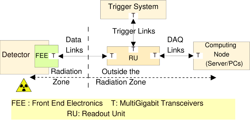
The RU acts as an interface between detector data links, the trigger system, and links to storage as well as computing nodes as shown in Figure 1. The tasks performed by the FPGA based RUs depend on the detector specifications and requirements. Main tasks are data sorting, optical link handling, multiplexing and forwarding of data from different interfacing links, embedding control and trigger information, etc. [14]. These versatile functionalities require RU to be designed on custom electronics boards with re-programmable functionality [15]. It is based on up-to-date FPGA technology with embedded on-chip transceivers. For our tests we have used the Intel Arria-10 GX FPGA based development board [11, 16]. The interfacing links of RU and the high-speed communication protocols used for the LHC experiments in the context of the present framework are discussed in the following sections.
3 High-speed protocols
The DAQ architecture in Fig. 1 features three different interfacing links: (i) the Data link, which connects the detector FEE to RU, (ii) the Trigger link, which connects the RU to the trigger system of the experiment, and (iii) the DAQ link, which takes the data from the RU to the storage and computing nodes. For the data link, the Gigabit Transceiver (GBT) protocol architecture [17], developed at CERN, has been found to be most ideal. The GBT protocol supports 4.8 Gb/sec data transmission rate. It ensures the transmission of data from the FEE near the detectors in high radiation zone to the RU, which is located near the counting room in a low or no radiation zone. The Trigger link uses the Timing, Trigger and Control system based on Passive Optical Networks (TTC-PON) technology [18]; operates at the rate of 9.6 Gigabit per second. It ensures fixed, deterministic latency and satisfies the timing specification of the LHC.
The data packets get time-stamped in the RU. Thus the links from the RU to the computing nodes is not latency critical. It has been found that the latest promising technology option of 10-Gigabit Ethernet [5] with ample ecosystem are most suitable for the DAQ links in the experiments. In Table 1, we give the detailed specifications of the three interface links used in the HEP experiments for the acquisition of data.
| Parameters | GBT | TTC-PON |
|
|||||||
| Technology Specification | Custom |
|
|
|||||||
| Designer Group | CERN |
|
IEEE | |||||||
| Line Rate | 4.8 Gbps |
|
|
|||||||
| Payload Rate | 3.2 Gbps |
|
|
|||||||
| Payload Size | 120 bits@40 MHz |
|
64 bits@156.25 MHz | |||||||
| Wavelength (nm) |
|
|
|
|||||||
| Network Topology | Point-to-Point | Point-to-Multipoint | Point-to-Point | |||||||
| Encoding |
|
8b/10b | 64b/66b | |||||||
|
Yes | Yes | No | |||||||
| Trigger Latency |
|
|
NA |
4 Transceiver optimization
High-speed data communication suffers from the transmission losses and signal integrity issues; not seen at normal digital signalling levels [10]. The high-frequency content of the signal gets degraded due to dielectric losses, skin effect, discontinuities in connectors, reflections caused by the vias, inadequately placed traces, etc. We have developed a technique to optimize the transceiver parameters accurately and offer the best combination for a given high-speed link. This optimization of the transceiver parameters could take care of the transmission losses [19].
For the high-speed transmission channels with multi-gigabit rates, the unit interval (UI) for the data bit decreases. At high transmission rates, the PCB materials suffer from frequency dependent losses, hence become dispersive. This prevents the signal from reaching its full strength at the shrunk UI window, leading to jitter and intersymbol interference (ISI). It also disturbs the deciphering of the signal and the extraction of the embedded clock becomes difficult at the receiver end.
An increase of the signal strength is an obvious solution to overcome the attenuation. However, the issue of high-frequency roll-off remains, and the pattern dependent jitter gets aggravated. Consequently, the signal does not reach its optimal strength within the interval and may diffuse further into the next UI leading to ISI. Also for the increase of signal strength overall power consumption of the transceiver increases. Noise levels in the system also increase proportionally. All these lead to deteriorated metrics of signal integrity and reduced drive length. The effects are even more evident with the use of high-speed interfaces with the systems which were originally designed for low bandwidth applications.
To overcome these losses, we have developed the transceiver optimization technique and a proficient methodology for 20nm Arria-10 FPGA. This new FPGA with considerably large on-chip resources [11] are ideal for the processing requiremnts in the experiments.
4.1 Optimization Technique
For the optimization, the high-frequency components in the data stream are boosted up on every switching, using the digital pre-emphasis taps of the on-chip transceiver. In addition, the low frequency components are reduced. This technique helps to achieve the same amount of emphasis with less power dissipation. The exaggerations are overridden by the attenuation during transmission and allow for the signal to be recovered accurately.
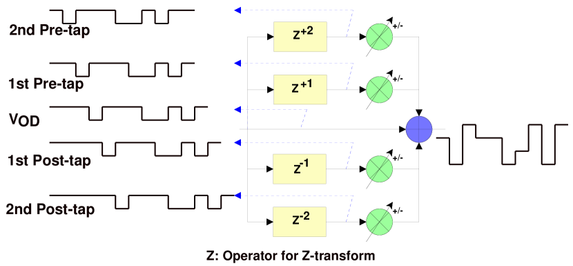
The optimization technique has been implemented on Intel Arria-10 FPGA development board with integrated reconfigurable transceiver architecture [11]. It incorporates additional circuitry in buffers for equalisation and pre-emphasis techniques. The transmitter of the embedded transceiver has five programmable drivers as shown in Figure 2. Voltage output differential (VOD) controls the base amplitude. The four pre-emphasis taps are 1st pre-tap, 2nd pre-tap, 1st post-tap and 2nd post-tap. These taps also include polarity settings. The post taps are the causal taps and the pre-taps are the anti-causal taps. These multiple taps and choice of polarity could handle channel attenuating characteristics. Equalisation with DC gain and Variable Gain Amplifier (VGA) is on the receiver side of the transceiver. There are multiple transceiver parameters with a large span of operating range and so to scan the system performance for every combination of the parameters is a time-consuming process. Our goal had been to develop an efficient technique for optimization of transceiver parameters such that the signals impacted by the high-frequency losses are recovered.
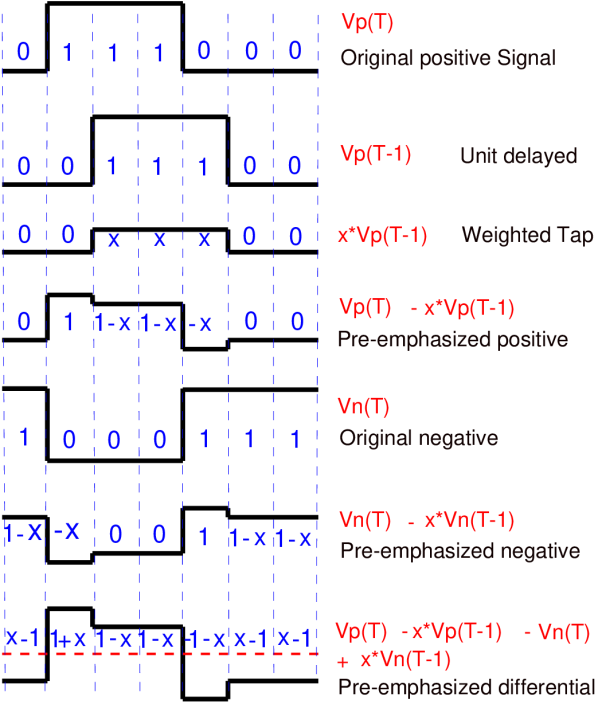
It works like a Finite Impulse Response (FIR) filter with different delays referred to as the taps as shown in the Figure 2. An FIR filter is based on a feed-forward difference equation. The pre-emphasis technique applies a delay to the signal and adds it back to the real signal with weight and inversion as and when required. Although depending on the transmission channel peculiarity, a simple delay, weight and inversion may not be able to provide the required compensation. For this reason, a combination of different delays, weights and the polarity are combined. In this configuration, the pre-emphasis 1st post-tap is the most useful parameter. It emphasises the immediate bit period after the transition. The generation of the differential emphasised signal, applying the unit delay by the first post-tap is shown in Figure 3, assuming VOD = 1 and tap weight as . The original positive signal Vp(T) is compared with Vp(T-1) which is the unit-delayed signal. The emphasised signal is the difference between the weighted x*Vp(T-1) signal and the Vp(T) signal. The negative signal is similarly generated. The pre-emphasised differential signal is differentiated from the positive and negative signals.
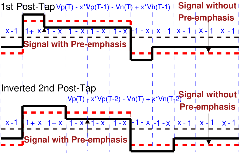
The effect of 2nd post-tap after the transition, depending on the chosen polarity setting is shown in Figure 4.
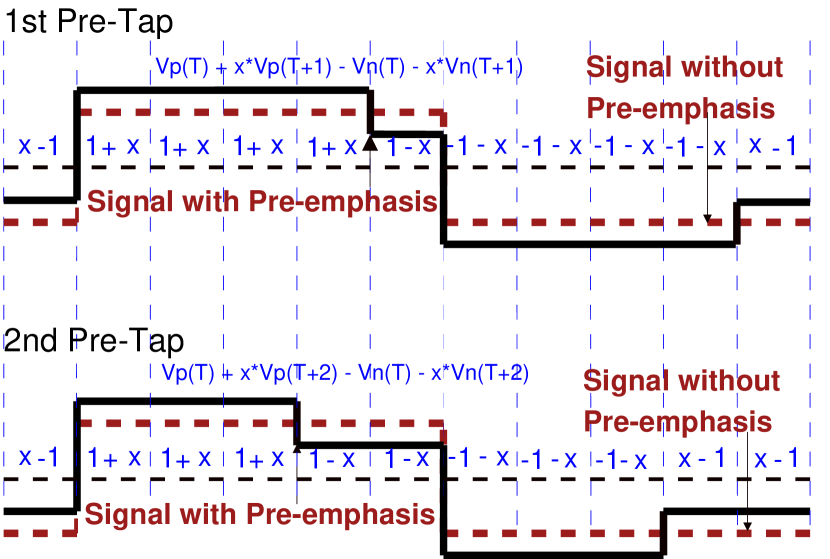
The pre-tap reduces the effect of pre-cursor ISI. Figure 5 shows the impact of 1st pre-tap and the 2nd pre-tap on the single and double bit period respectively, before the occurrence of high-frequency transition depending on the polarity. Both pre-cursor ISI and post-cursor ISI are handled by anti-causal and causal taps respectively. However, pre-emphasis alone cannot guarantee the performance of the system as it is implemented at the transmitter by pre-conditioning the signal before it is fed to the channel. There are high-frequency losses in the transmission channel itself. Hence an equalisation is required at the receiver end. It compensates for the low pass characteristics of the physical medium and amplifies the attenuated high-frequency components of the incoming signal. An equalizer on the receiver side lifts the contents inside a band of frequencies and attenuates the rest. The DC gain circuitry gives uniform amplification to the received spectrum. It enables the transceivers to operate over longer distances. The VGA on the receiver optimizes the signal amplitude before the CDR sampling.
To achieve an optimal signal integrity performance, both transmitter and receiver parameters of the transceiver on FPGA chip augments each other and work combined to compensate for the high-frequency losses. However, the overcompensation degrades the signal quality and adds more jitter leading to the closed eye diagram rendering it futile for the receiver to identify the signal and hence should be avoided.
5 Test setup
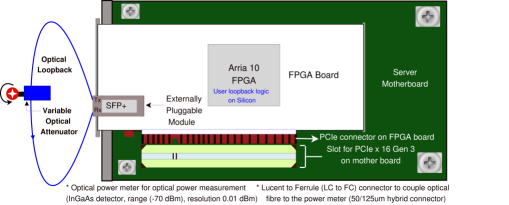
An FPGA based setup has been developed to test the potency of the proposed optimization technique. The transceiver is tested for the high-speed links under the stressed conditions. The setup has been utilised to emulate the stressed high-speed link conditions and to investigate the high frequency losses in the transmission. It determines the capability of the transceiver system to recover the data from the degraded signals. Tests are performed at the system level to operate the setup at a prescribed BER equal to or better than as per the IEEE standard.
The test setup, shown in Fig. 6, engrosses the Arria-10 FPGA development board (10AX115S2F45I1SG device) for the implementation and testing of the optimization technique. The FPGA development card is installed on the PCIe 16 lane slot of the server, where the power is obtained from the server motherboard. The functions and specifications of each of the components of the setup are given in Table 2.
| Component | Role in test setup | Specification | ||||||||||
|---|---|---|---|---|---|---|---|---|---|---|---|---|
| FPGA Test Board |
|
|
||||||||||
|
|
|
||||||||||
|
|
|
||||||||||
|
|
|
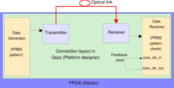
Intel Quartus-II platform is the firmware application package, implemented on the FPGA logic design. The transmission links at the specified data rates are implemented using Quartus-II Qsys tool. Qsys is Intel′s system integration tool for the quick generation of the interconnect logic. The signal integrity of the transceiver links is validated using Transceiver Toolkit (TTK) feature of Quartus-II with a GUI. The TTK is used to quickly access, tune and test the transceiver parameter settings in runtime through a combination of metrics. The TTK enables us to measure BER and the eye diagrams and also verify the signal integrity in external loopback mode. Details of the firmware-tools, such as, Quartus II, Qsys, TTK, PRBS patterns and auto-sweep features may be found in reference [12].
For the data loopback tests [21], multimode optical fibre equipped with Variable Optical Attenuator (VOA) and external pluggable SFP+ modules are used. The far end of the transceiver is coiled back to the receiving end. The received data is then verified by the data checker logic on FPGA for any erroneous bits as shown in Figure 7. To test the signal integrity a variety of data patterns can be used. However, in each case, a checker must be available for verification. PRBS patterns are injected into the test system as it generates the stressed and lengthy patterns with fewer memory consumption [22]. Another advantage of using PRBS patterns for the tests is that the boundary synchronisation is not necessary at the physical layer as the patterns are time correlated. The Intel soft logic cores are used for PRBS data pattern generator and checker [12].
The BER measurement approach was chosen with respect to the controlled attenuated optical power at the receiver with the help of VOA. It allowed us to rapidly characterise the transceiver sensitivity below which the embedded clock cannot be recovered from the data stream, and loss of lock occurs [19]. It also determines the minimum required optical power to achieve the targeted BER for a system operating at a specified data rate. Auto sweep feature of TTK is used to obtain the optimum settings of the best performing parameters of the transceiver for a specified BER. This optimized set of transceiver parameters delivers the best metrics of signal integrity and the eye diagrams by its height and width. In the next section, we elaborate the methodology for the optimization of high data rate on-chip transceivers to reduce the effect of high-frequency losses.
6 Methodology
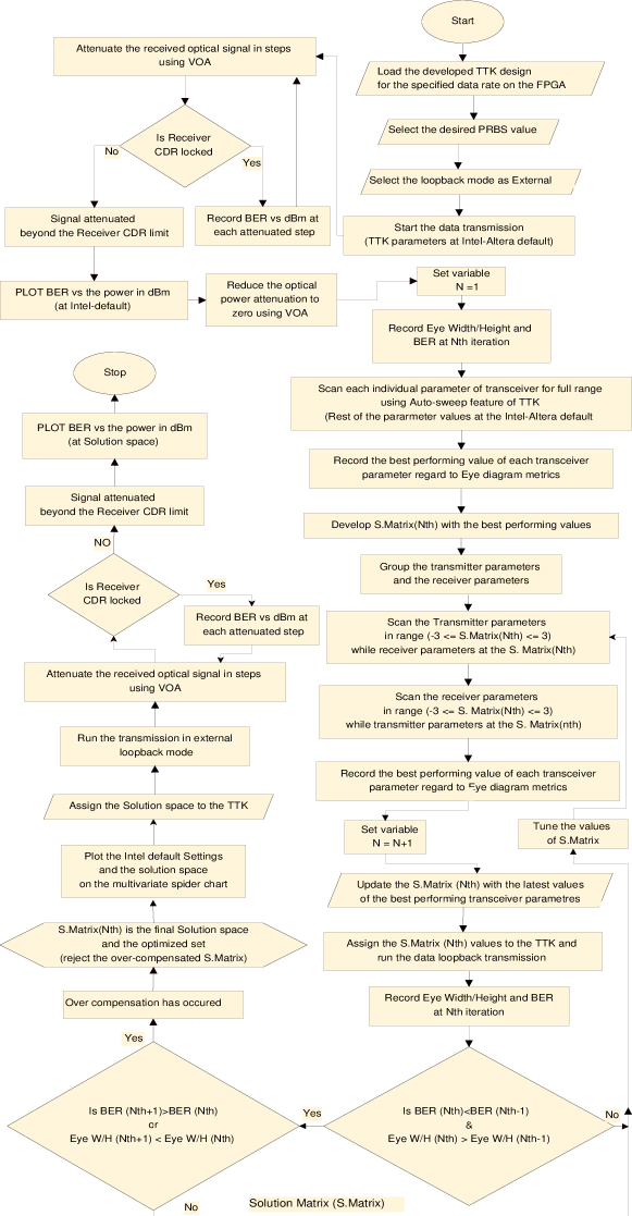
The methodology to extract the optimized settings of the transceiver parameters has been explained in the flowchart in Figure 8. To start with, the optimization process scans the full range of each transceiver parameter using the TTK auto-sweep feature while the rest of the parameters are set at their Intel-default values. Then it records the best performing tap setting values for each transceiver parameter as indicated by eye parameters. At this instance, a Solution Matrix at iteration, set is developed. Then, we separately group the transmitter parameters viz. VOD, Pre-emphasis (1st pre-tap, 2nd pre-tap, 1st post-tap, 2nd post-tap) and the receiver parameters (DC gain, Equalisation control, VGA). Then we scan again the transmission and receive parameters separately in the range of -3 S 3, while receive and transmit parameters respectively are set at the values enlisted in the S. Record again the best performing cases and update the S with newer values, increment N by 1. Assign the latest matrix values to the TTK and run the loopback test. If this does not result in the improved metrics of signal integrity (Eye diagram and the BER) than the one obtained at the Intel default set values; repeat the optimization loop with the adjusted S values in the range defined until the improvement in both eye diagram and BER is achieved.
The parameters cannot be declared as optimized until a stage of degradation in the signal integrity metrics from their peak values is observed. The degradation of metrics denotes the over-compensation and it marks the transition from the maxima of the transceiver parameters. Assign and update the S with the best performing case metric values rejecting the over-compensated value set. The final S values with the best performing metrics is known as Solution Space [19]. The deduced final values are fed to the transceiver for further analysis. The results are presented and discussed in the next section.
The proposed technique has definite advantages over traditional method where the transceiver optimization may be carried out in an extremely time-consuming way by evaluating the signal integrity through a large number of permutations and combinations of the parameters. The parameters and their possible ranges are listed in the Table 3.
|
|
|
||||||||
| Transmitter Side | ||||||||||
| VOD | 0 to 31 | 32 | ||||||||
| Pre-emphasis 1st post-tap | -31 to 31 | 63 | ||||||||
| Pre-emphasis 1st pre-tap | -31 to 31 | 63 | ||||||||
| Pre-emphasis 2nd post-tap | -15 to 15 | 31 | ||||||||
| Pre-emphasis 2nd pre-tap | - 7 to 7 | 15 | ||||||||
| Receiver Side | ||||||||||
| DC gain | 0 to 4 | 5 | ||||||||
| Equalisation | 0 to 15 | 16 | ||||||||
| VGA | 0 to 7 | 8 | ||||||||
7 Results and discussion
Results are demonstrated and validated for the three different high speed optical links: 10 Gbps links, 4.8 Gbps GBT protocol and 9.6 Gbps TTC-PON. The test system confronts the lock and hold capability of the CDR circuit, perturbs all the conceivable instances of ISI and analyses the receiver sensitivity for any probable drifts. Drifts at the receiver are caused due to long imbalanced runs of the data transition pattern. The PRBS31, patterns integrate every alteration of 31 bits. It gives a random sequence of bits with high and low transitional values as defined by the logic levels of FPGA. The different combinations induce non-similar ISI configurations. It is required to stress the transceivers, test any innate ISI in a transmitter, and to assess the quality of transmission. PRBS patterns depict a white spectrum in the frequency domain and are injected to tests the robustness of the high-speed links. For the entire analysis, PRBS31 is used to stress the system. However, the variation of eye diagram and BER characteristics are also studied for PRBS7, PRBS9, PRBS15, PRBS23 in addition to PRBS31.
7.1 Eye Diagram analysis
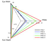
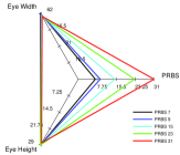
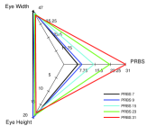
At the system startup, the transceiver parameters in TTK are set at the default values. Changes in eye diagram are compared for different PRBS stressed patterns as the first set of analysis. Eye Height and Width is plotted on a three axes plot with PRBS pattern on the third axes as shown in Figure 9. It is found that PRBS31 has the most stressed eye metrics and as anticipated a more closed eye is examined for all the three links speed.
 |
| 10 Gbps |
 |
| GBT 4.8 Gbps |
 |
| TTC-PON 9.6 Gbps |
7.2 BER Results
Another important metric of signal integrity is BER. Its measurement is a statistical phenomenon and the estimate is ideal only if the number of tested bits tends to infinity, which is not possible in a real lab test setup. Hence, a method was proposed in reference [23] to limit the stressing time of a system to a feasible length and to measure the BER with high confidence level (CL) too. CL is used to quantify the quality of the estimate in percentage. It is the system’s actual probability of error less than the specified limit. The minimum number of bits required to be tested for the BER measurement with a specific associated CL is given in equation 3:
| (3) |
is test time needed, is the line rate and when the solution is trivial given in equation 5.
| (5) |
Where are the total number of bits transmitted and are the number of errors that occurred during the transmission. There is a compromise between testing time and the required accuracy of the measurement as shown in equation 3.
For the 95 percent CL, equation 5 reduces to n . Hence to achieve the BER of at 95 percent CL, total 3x bits need to be tested, as a thumb rule.
7.2.1 BER analysis for various link speeds
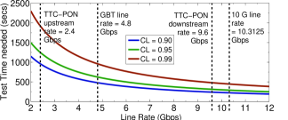
The concept is further extended to find the minimum inspection time required to measure BER of for different CL with no errors for GBT, TTC-PON and 10 Gbps links as shown in Figure 10. In this paper, all the BER measurements are done for 3x bits to achieve 95 percent CL.
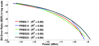
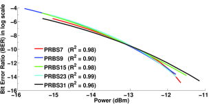
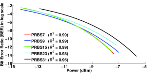
Variation of BER at Intel-default transceiver set is recorded with respect to the attenuation of the received optical power; following the methodology flowchart shown in Figure 8. This test is executed with the help of VOA attached to the loopback fibre. BER variation is recorded for different PRBS patterns and plotted for the links operating at 10 Gbps, 4.8 Gbps and 9.6 Gbps rates as shown in Figure 11.
 |
| 10 Gbps |
 |
| GBT 4.8 Gbps |
 |
| TTC-PON 9.6 Gbps |
The exponential curve fitting is the best-suited approximation for the BER in logarithmic domain [24]. Double exponent fit function with constants is used to fit the BER data as it provides close fits in a variety of BER plot situations. It fits the BER data using unconstrained nonlinear optimization [25]. The statistics for goodness-of-fit in terms of R-Square () for different PRBS is marked in the Figure 11.
The test shown in Figure 11 highlights that at a specified CL higher number of errors are received in the transmission system for a given received optical power; when PRBS31 is injected as the test data pattern as compared to the other PRBS patterns. The outcome of the tests shown in Figure 9 and Figure 11 revealed the degradation of the metrics of signal integrity with the increase in the size of a unique word of data in the PRBS sequence. The results from these tests are as anticipated and well substantiated. It has further strengthened the usefulness of the PRBS31 as a strenuous test pattern to demonstrate the validation of the proposed methodology. However, there is a crossover point for 4.8 Gbps at BER. It is kept beyond the discussion as our region of interest is better by two orders of magnitude which is BER.
7.3 Improvement in Transmission
The improvement in the system performance is marked by two metrics of signal integrity viz. BER and Eye Diagram. The eye contour for the Intel-default settings and at the deduced optimized settings of the transceiver is captured using the EyeQ (a GUI feature of TTK). It helps to estimate and visualize the vertical and horizontal eye opening at the receiver as shown in Figure 12. After the application of the deduced transceiver parameter’s settings using the proposed technique, there is a notable enhancement in width (Horizontal Phase Step) and height (Vertical Step) of the eye diagram. Hence the quality of signal transmission is improved.

Vertical step(19)/Horizontal Phase step(41) for 10 Gbps at the Intel FPGA default settings

Vertical step(49)/Horizontal Phase step(54) for 10 Gbps at the Optimized FPGA settings

Vertical step(28)/Horizontal Phase step(59) for 4.8 Gbps at the Intel FPGA default settings

Vertical step(63)/Horizontal Phase step(63) for 4.8 Gbps at the Optimized FPGA settings

Vertical step(18)/Horizontal Phase step(43) for 9.6 Gbps at the Intel FPGA default settings

Vertical step(41)/Horizontal Phase step(50) for 9.6 Gbps at the Optimized FPGA settings
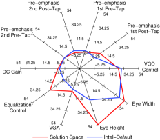
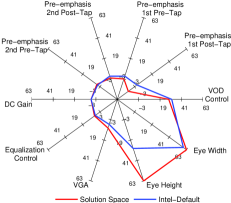
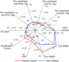
The optimized values of the transceiver parameters known as solution space, found from the proposed methodology for the targeted BER of are plotted against the Intel-default set in the form of a multivariate kiviat diagram for all the three link speeds as given in Figure 13. It allows us to demonstrate a clear comparison of the individual parameters on each axis.
10 Gbps line rate
GBT 4.8 Gbps line rate
TTC-PON 9.6 Gbps line rate
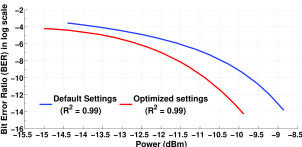
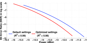
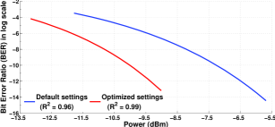
Variation in BER is plotted for the deduced solution space values of a transceiver and for the Intel default set; concerning the different attenuation levels of input optical power at the receiver. It is shown for PRBS31 for all the three links under observation in Figure 14.
10 Gbps line rate
GBT 4.8 Gbps line rate
TTC-PON 9.6 Gbps line rate
Further analysing the results from Figure 14, the least optical power required at the receiver to attain a preferred BER or better could be determined from the curve. Also it shows, that a specific marked BER is achieved at a lower optical power when transceiver is operated at the deduced parameter values listed in solution space in comparison to the Intel default set. Here to mention the particular case as an example, the targeted BER of for the optical link test as per IEEE standards is achieved at lower values of the optical power and the improvement at the mentioned BER is quantitatively listed in Table 4 for the three link speeds.
|
|
|
|
|
|||||||||||
|---|---|---|---|---|---|---|---|---|---|---|---|---|---|---|---|
| 10Gb Ethernet | -9.2 | -10.35 | -1.15 | 12.5 | |||||||||||
| GBT | -11.9 | -12.7 | -0.8 | 6.7 | |||||||||||
| TTC-PON | -6.45 | -9.3 | -2.85 | 44.1 |
Another clear observation emerged from the data comparison of Figure 14 is that the receiver sensitivity below which the loss of lock occurs, is enhanced due to the reduction in the high-frequency losses with the application of the proposed optimization technique. This results in reducing the limit of the optical power required for the proper CDR and the signal is traceable for comparatively lower values of the received optical power. The quantitative comparisons are given in Table 5.
|
|
|
|
|
|||||||||||
|---|---|---|---|---|---|---|---|---|---|---|---|---|---|---|---|
| 10Gb Ethernet | -14.4 | -15 | -0.6 | 4.17 | |||||||||||
| GBT | -15.34 | -16.04 | -0.7 | 4.56 | |||||||||||
| TTC-PON | -11.78 | -13.2 | -1.42 | 12.05 |
The test results shown in Figure 13 and 14 confirms that the effect of high-frequency losses on the link performance is controlled. It is achieved after the application of the deduced solution space values to the TTK and a significant improvement on the BER is noted at a particular received optical power. The tests and results validate the usefulness of the proposed technique to enhance the transceiver performance and the signal integrity by compensating for the high-frequency losses.
8 Summary
We have presented a novel transceiver optimization technique to reduce the high-frequency losses which occur due to the increased rates of data transmission in case of HEP experiments. The technique has been implemented on the latest 20nm Intel-Altera Arria-10 FPGA. The scheme has been tested and validated for the link rates of three high-speed communication protocols, GBT, TTC-PON and 10 Gbps Ethernet, which are most commonly used for interfacing the detector front-end electronics, trigger and DAQ systems. The proposed scheme is an optimized approach which reduces number of iterations required.
The tests are performed with PRBS31 pattern at a confidence level of 95 percent. There is considerable gain in the system performance with the application of the proposed technique as specified by the two parameters of signal integrity, the BER and the Eye Diagram. The Intel FPGA set parameters and the solution space values are marked on the kiviat diagram for the fast comparison between the parameters. The results point that to attain the marked BER of ; the required optical power is reduced by 12.5%, 6.7% and 44.1% for 10Gbps, GBT and TTC-PON respectively. The BER is also improved over the received range of optical power. The CDR capability of the system is also enhanced as the least optical power required to recover the data traffic is reduced by 4.17%, 4.56% and 12.05% for 10Gbps, GBT and TTC-PON respectively. The technique improves the signal integrity and reduces the BER. This technique is a heuristic solution and has potential for practical applications as it provides rapid convergence of the solution space to achieve optimized transceiver settings. It makes the implementation of the new technique time efficient. This transceiver optimization technique and its implementation approach would lend itself well for other FPGAs users that allows on-chip assessment of signal quality like Eye diagram.
Acknowledgement
The authors gratefully acknowledge the support of the ALICE Collaboration at CERN during the period of the research work. We thank Alex Kluge, Tivadar Kiss, Erno David of the ALICE Electronics coordination and the CRU project for their valuable help and advice. We thank Subhasis Chattopadhyay, Anurag Misra and Saurabh Srivastava for fruitful suggestions during the preparation of the manuscript.
References
- [1] D. E. Morrissey, T. Plehn, T. M. Tait, Physics searches at the LHC, Physics Reports 515 (1-2) (2012) 1–113.
- [2] W. K. Panofsky, Evolution of particle accelerators, SLAC Beam Line 27 (1997) 36–44.
- [3] W. Smith, Trigger and data acquisition for hadron colliders at the energy frontier (2013), arXiv preprint arXiv:1307.0706.
- [4] S. A. Khan, J. Mitra, E. David, T. Kiss, T. K. Nayak, A potent approach for the development of FPGA based DAQ system for HEP experiments, Journal of Instrumentation 12 (2017) T10010.
- [5] J. Toledo, F. Mora, H. Müller, Past, present and future of data acquisition systems in high energy physics experiments, Microprocessors and Microsystems 27 (2003) 353–358.
- [6] J. Mitra, S. A. Khan, et al., Common readout unit (CRU)-a new readout architecture for the ALICE experiment, Journal of Instrumentation 11 (2016) C03021.
- [7] Gutiérrez, et al., The ALICE TPC readout control unit, in: Nuclear Science Symposium Conference Record, Vol.1, IEEE 2005, Vol. 1, 2005, p. 575.
- [8] S. A. Khan, J. Mitra, T. K. Nayak, Development of a high speed data acquisition system for the detectors at high luminosity LHC, in: Proceedings of the XXII DAE High Energy Physics Symposium, Springer, 2018, p. 223.
- [9] B. Razavi, Challenges in the design high-speed clock and data recovery circuits, IEEE Communications magazine 40 (2002) 94–101.
- [10] S. H. Hall, H. L. Heck, Advanced signal integrity for high-speed digital designs, John Wiley & Sons, 2011.
- [11] I. Altera, Intel Arria 10 Device Overview (2018).
- [12] I. Altera, Quartus Prime Standard Edition Handbook Volume 1: Design and Synthesis (2017).
- [13] G. F. Knoll, Radiation detection and measurement, John Wiley & Sons, 2010.
- [14] L. Li, A. M. Wyrwicz, Parallel 2D FFT implementation on FPGA suitable for real-time MR image processing, Review of Scientific Instruments 89 (9) (2018) 093706.
- [15] S. G. Castillo, K. B. Ozanyan, Field-programmable data acquisition and processing channel for optical tomography systems, Review of scientific instruments 76 (9) (2005) 095109.
- [16] Intel Corporation, Arria 10 FPGA Development Kit User Guide (2017).
- [17] M. B. Marin, S. Baron, et al., The GBT-FPGA core: features and challenges, Journal of Instrumentation 10 (2015) C03021.
- [18] E. Mendes, S. Baron, D. Kolotouros, C. Soos, F. Vasey, The 10G TTC-PON: challenges, solutions and performance, Journal of Instrumentation 12 (2017) C02041.
- [19] I. Altera, High-SpeedLink Tuning Using Signal Conditioning Circuitry in Stratix V Transceivers (2015).
- [20] S. Committee, et al., SFF-8431 Specifications for Enhanced Small Form Factor Pluggable Module SFP+, revision 4.1, July 6, 2009.
- [21] S. I. Green, Multichannel bit error rate tester for fiber optic transceiver testing, Review of scientific instruments 73 (8) (2002) 3125–3127.
- [22] H. Badaoui, Y. Frignac, P. Ramantanis, B. E. Benkelfat, M. Feham, PRQS Sequences Characteristics Analysis by Auto-correlation Function and Statistical Properties, IJCSI (2010) 39.
- [23] D. Mitić, A. Lebl, Ž. Markov, Calculating the required number of bits in the function of confidence level and error probability estimation, Serbian Journal of Electrical Engineering 9 (2012) 361–375.
- [24] L. J. Ippolito, Appendix b: Error functions and bit error rate, Satellite Communications Systems Engineering: Atmospheric Effects, Satellite Link Design and System Performance 363–366.
- [25] S. Chapra, R. P. Canale, Numerical methods for engineers : with personal computer applications / steven c. chapra, raymond p. canale.