Timing performance of small cell 3D silicon detectors
Abstract
A silicon 3D detector with a single cell of m2 was produced and evaluated for
timing applications. The measurements of time resolution were performed for 90Sr electrons with
dedicated electronics used also for determining time resolution of Low Gain Avalanche Detectors (LGADs).
The measurements were compared to those with LGADs and also simulations. The studies showed that the
dominant contribution to the timing resolution comes from the time walk originating from different
induced current shapes for hits over the cell area. This contribution
decreases with higher bias voltages, lower temperatures and smaller cell sizes. It is around
30 ps for a 3D detector of m2 cell at 150 V and -20∘C, which is comparable
to the time walk due to Landau fluctuations in LGADs. It even improves for inclined
tracks and larger pads composed of multiple cells. A good agreement between
measurements and simulations was obtained, thus validating the simulation results.
PACS: 85.30.De; 29.40.Wk; 29.40.Gx
keywords:
Silicon detectors, Radiation damage, Signal multiplication, Time measurements1 Introduction
The choice of solid state timing detectors to be used at large experiments CMS [1] and ATLAS [2] after the luminosity upgrade of the LHC (HL-LHC) are presently thin Low Gain Avalanche Detectors (LGAD) [3]. They rely on charge multiplication in the so called gain layer, a heavily doped 1-2 m thick layer sandwiched between the implant and the bulk. Gains of allow efficient operation of thin detectors ( m) required for superior time resolution [4] of around 30 ps per detector layer [5].
However, the gain degrades with irradiation [6, 7]. The high gain of LGADs can be maintained at equivalent fluences below cm-2, where their performance has been demonstrated to fulfill the HL-LHC requirements [8]. At fluences above that, particularly of charged hadrons, the operation requires extremely high bias voltages of V to achieve small gain factors (of only few) [7]. With the loss of gain and consequent decrease of signal-to-noise ratio () the time resolution and detection efficiency of thin LGADs degrades. Operation of LGADs close to breakdown voltage poses a risk and so far there is also no running experience over years of operation.
Another problem of LGADs are special junction termination structures used to isolate pixels/pads and prevent early breakdowns, which lead to a region between pixels/pads without the gain [9]. This region has typically a width of the order of 40-100 m, which even for relatively large pads of mm2 leads to a significant reduction of a fill factor of up to 13%. More importantly, this prevents using LGADs with smaller pads, which would be required for a smaller pad/pixel capacitance. The fill factor can be resolved by using so called inverse LGADs (iLGAD) [10], which however require even more complex processing. A problem of decreasing gain with irradiation is only moderately improved by the carbon co-implantation in gain layer [11] or replacement of boron with gallium [11, 12]. As a result of the above mentioned limitations of LGADs alternatives are sought.
Recent results with 3D detectors produced by CNM111Centro Nacional de Microelectrónica (IMB-CNM-CSIC), Barcelona, Spain, which have a cell size compatible with the RD53 readout chip[13], both in test beam [14] and with 90Sr electrons [16, 17], showed only small degradation of charge collection with fluence over the entire HL-LHC fluence range, with most probable signal e for 230 m thick detector. Efficient charge collection together with small drift distances, which lead to short induced current pulses, offer a possibility for their use also in timing applications.
The aim of this paper is an investigation of small cell 3D detectors in timing applications. Simulations and measurements with 90Sr electrons will be discussed in the work.
2 Time resolution
The time resolution () of a detector is to a large extent given by
| (1) | |||||
| (2) |
where is the jitter contribution determined by the rise of the signal at the output of the amplifier and noise level ( is peaking time of electronics and signal to noise ratio) and is the time walk contribution. The latter is usually minimized by using Constant Fraction Discrimination or determining time of the signal crossing fixed threshold and its duration over that threshold. These two techniques eliminate the difference in signal height arising from the amount of deposited charge in the sensor, but not the differences in signal shapes. The shape of the signal is mainly affected by the differences in drift paths (depending on the hit position hit positions inside the pixel cell) of generated carriers, which drift with different drift velocities in different weighting fields. Fluctuations in ionization rates along the track path (Landau fluctuations) add to the differences in pulse shapes. These two contributions usually dominate the time walk.
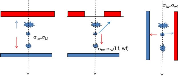
For planar detectors with thickness cell size the weighting field is constant over the entire cell and cannot cause any differences in signal shape (see Fig. 1). Hence, the time walk is dominated by Landau fluctuations (), particularly for LGADs where electrons need to reach the gain layer to multiply. For fine segmentations, careful test beam studies can be used to separate both contributions, such as for the NA62 pixel detectors [18]. In 3D detectors Landau fluctuations are less important as charges generated at different depths have the same drift distance to the collection electrode. The time walk contribution is therefore dominated by the location of impact within the cell (). This isn’t entirely true for inclined tracks, but absence of gain and short drift distances render to be negligible.
(a) (b) (c)
3 Simulation of detectors
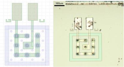
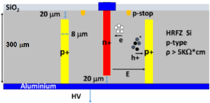
A special structure produced by CNM was used in the studies and is shown in Fig. 2a. A single 50x50 m cell with an readout electrode (1E) was surrounded by eight neighboring cells connected together. The thickness of the investigated detector was 300 m with a type bulk resistivity of 5 kcm. The diameter of the holes was 8-10 m. The junction columns were etched from the top while the four ohmic columns at each corner of the cell were etched from the bottom. Both column types penetrate some 20 m short of the full thickness as shown in Fig. 2b.
 |
 |
| (a) | (b) |
The software package KDetSim [19] was used to simulate the charge collection in such 3D detector. The package solves the three dimensional Poison equation for a given effective doping concentration to obtain the electric field and the Laplace equation for the weighting field. The induced current is calculated according to the Ramo’s theorem [20], where the charge drift is simulated in steps with diffusion and trapping also taken into account. The minimum ionizing particle track was split into “buckets” of charge 1 m apart. The drift of each bucket was then simulated and the resulting induced current is the sum of all such contributions. The details of the simulation can be found in several references [21, 22]. The simulated induced current is then processed with a transfer function of a fast charge integrating preamplifier followed by a CR-RC3 shaping circuit with a peaking time of 1 ns.
 |
 |
| (a) | (b) |
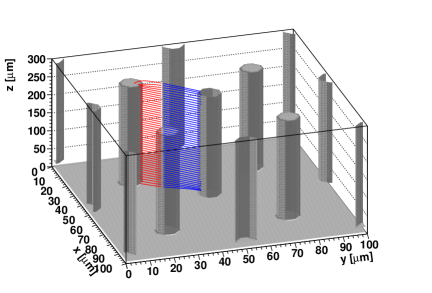
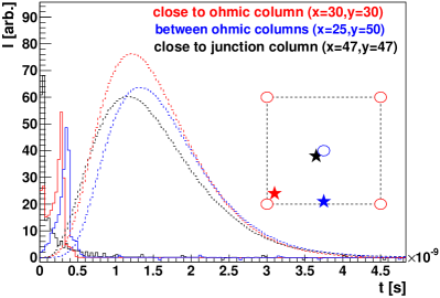
An example of a minimum ionizing particle hitting the cell is shown in Fig. 3a. The drift paths of electrons (blue) to junction column and holes (red) to ohmic columns are shown. The obtained induced currents for three different hit positions indicated in the picture (solid lines) and the signal after electronics processing (dashed lines) are shown in Fig. 3b. In the simulation the constant fraction discrimination with 25% fraction was used to determine the time of arrival (ToA). A charge of at least 1000 was required to actually calculate the time stamp of the hit (the hits with less have ToA=0). Several different amplification circuit models (CR-RCn) were used with different peaking times which all yield similar results.
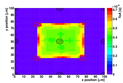
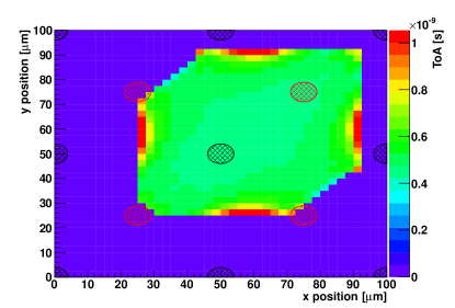
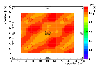
ToA for perpendicular tracks with impact positions distributed across the cell are shown in Fig. 4a. As expected the signal for tracks hitting the regions with a saddle in the electric field (between ohmic and junction electrodes) showed a delayed ToA. En example of ToA map for ionizing particles under angle is shown in Fig. 4b.
The histogram of ToA over the cell surface for both cases is shown in Fig. 4c. The width of the Gaussian fit to the peak of the distribution is an estimate of the hit-position contribution to the time resolution (). The distribution is not symmetrical and has a tail which is larger for a larger angle, although the Gaussian width is smaller. The hit position contribution is ps for perpendicular tracks and 51 ps for tracks under an angle of 5∘ at 50 V and room temperature. Decrease of the temperature improves the time resolution substantially as shown in Fig. 4d, due to a faster drift.
 |
 |
| (a) | (b) |
 |
 |
| (c) | (d) |
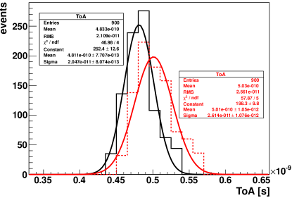
The distributions in Figs. 4 refer to the case where the cells are read out separately. If multiple cells are connected together then the charge sharing, which reduces a single cell signal, does not occur and a much narrower distribution is obtained without tails as can be seen in Fig. 5. Around ps is obtained for inclined tracks () at 50 V already at room temperature and ps at -20∘C.
 |
 |
| (a) | (b) |
The simulation was used to predict the time resolution limits () for different cell sizes, temperatures and doping concentrations. In this study separately readout square cells with a single junction column (1E) were assumed. The simulation was done for perpendicular tracks at a temperature of -20∘C. Instead of the width from a Gaussian fit a more conservative estimation, RMS of the ToA distribution was used as .
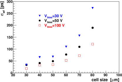
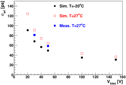
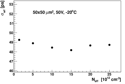
The dependence of on cell size is shown in Fig. 6a for different bias voltages. For large cell sizes the time resolution degrades rapidly, particularly at small bias voltages. The faster drift time at lower temperatures improves the time resolution for a m2 cell as shown in Fig. 6b. At 50 V ranges from 46 ps at -20∘C to 63 ps at 27∘C. At even higher bias voltages of 100 V ps is achieved. Almost no influence of wafer doping concentration on is predicted by simulations as shown in Fig. 6c.
 |
 |
| (a) | (b) |
(c)
4 Measurements
The experimental setup is shown in Fig. 7. Electrons from 90Sr source (=2.3 MeV) were used to determine the time resolution of the test-structure shown in Fig. 2a. The central columns ()of two such test-structures 400 m apart were connected together to the input of the amplifier, while the neighboring electrodes were grounded. The first stage of amplification uses fast trans-impedance amplifier designed by UCSC [15] followed by a second amplifier which gives signals large enough to be relatively easily recorded by a 40 GS/s digitizing oscilloscope with 2.5 GHz bandwidth.
The reference time required for measurement of the time resolution was provided from a non-irradiated LGAD detector produced by HPK [7, 15]. It is m thick, has a diameter of 0.8 mm and high gain of at 330 V and room temperature. The time resolution of HPK-50D sensors was measured (in the same setup with a method described below) by using two such detectors and was determined to be 26 ps. More details on timing and charge collection measurements with these LGADs can be found in [7, 15]. The electrons were collimated to an angle of by a combination of collimator, small cell size and the circular opening in the PCB boards hosting the sensors.
The trigger was provided by the reference LGAD sensor, but due to small surface of the 3D detector (m2) the signal equivalent to half of the most probable signal, corresponding to five times the noise, was required in the 3D detector as well. Without that requirement the majority of triggers would be without hits in the 3D detector. The measurements were done at room temperature for both sensors. The 3D detectors used in the measurements had a breakdown votlage of slightly more than 50 V which prevented studies at higher voltages.
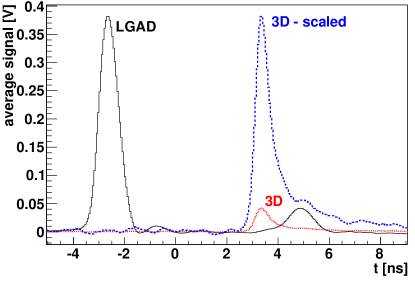
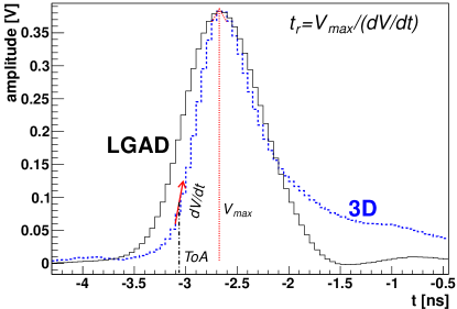
The comparison of averaged pulses from LGAD and 3D detector is shown in Fig. 8a. Apart from the obvious difference in height due to a large gain of the LGAD, the difference in both pulse shapes can be noticed. The slew rate is steeper for the 3D detector (see Fig. 8b), which however exhibits a longer tail.
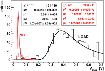
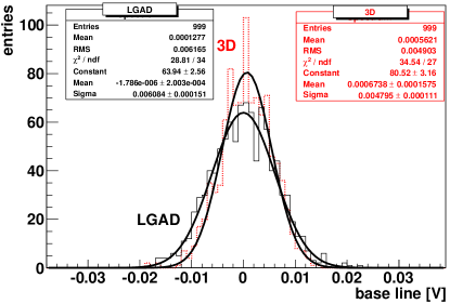
The spectrum of deposited charge, measured as amplitude of the signal , for the LGAD and the 3D detector are compared in Fig. 8c. The fit of the convoluted Landau and Gaussian distributions to the data is also shown. The difference of factor was observed in the most probable signal (parameter of the fit) which is also expected from the measured gain [7] and the difference in the detector thickness. As the noise level is 20% larger for LGAD, due to higher capacitance (see Fig. 8d), the difference in is by a factor of .
 |
 |
| (a) | (b) |
 |
 |
| (c) | (d) |
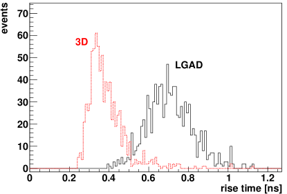
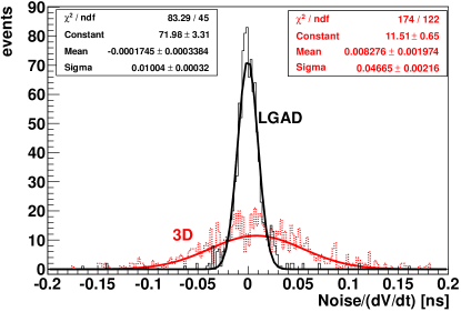
Faster rise time of the signal for the 3D detector is beneficial as it leads to a smaller jitter. For each event the rising edge was fitted with linear function around ToA () and the rise time was determined as (see Fig. 8b). The distribution of the rise times is shown in Fig. 9a. Such 3D detectors have therefore the rise time around two times shorter than 50 m thick LGADs. This is also reflected in the jitter measurement shown in Fig. 9b. The measured jitter for LGAD detectors ( ps) is 4.7 times smaller than that of the 3D detector ( ps). This is in agreement with Eq. 2 when the difference in average rise time by a factor of 1.75 and in by a factor of 8.5 is used.
 |
 |
| (a) | (b) |
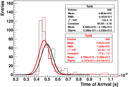
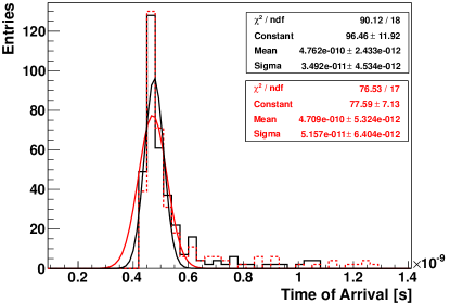
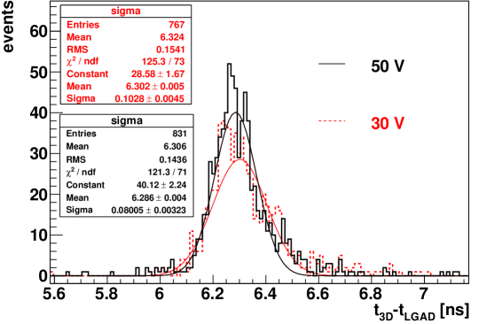
The time resolution was measured as the difference in ToA between LGAD (reference detector) and the 3D detector. As in simulation, ToA was measured when 25% of the maximum signal was reached (CFD). The distribution of the time difference is shown in Fig. 10 for 30 V and 50 V. It was fit with Gaussian function and the extracted was used as the time resolution of the measurement. It is given by
| (3) |
The time resolution of LGAD detector is ps ( ps, ps) therefore is dominated by the time resolution of the 3D detector () with and . With known , can be calculated as
| (4) |
which gives and . This agrees within 10% with the simulated values of 54 ps and 89 ps shown in Figs. 4c and 6b. Moreover, the tail in the timing distribution predicted in simulations is also observed in the measurements.
5 Discussion
A good agreement between measurements and simulations can be used to predict the operation also after irradiations. Charge collection measurements in similar pixel detectors showed a degradation by only a few percent at 175 V for 230 m thick detectors irradiated to an equivalent fluence of cm-2 [16]. Also a superb detection efficiency of was measured in test beam even after cm-2 at very high bias voltages of 200 V [14].
The increase of the breakdown voltage with irradiation will improve the timing performance. If at the same time charge collection degradation is small and sufficient cooling is provided to keep also the leakage current and shot noise small, the timing resolution of irradiated detectors may even surpass that of the non-irradiated one. Even more so, if 3D detectors will be operated in charge multiplication mode [16].
At the same time 100% fill factor can be maintained with 3D detectors. If larger cells are used the will even improve, particularly for angled tracks. The can be even significantly lower than for LGAD detectors.
In spite of somewhat shorter rise time, lack of sizable multiplication and consequently smaller means that jitter contribution to time resolution is relatively more important and possibly even dominant. For a typical rise time of ps a is required for , which for a 300 m thick silicon 3D detector translates to an equivalent noise charge of . Keeping the noise small is therefore of utmost importance, probably excluding large pad detectors with small cell size due to its larger capacitance. The capacitance of a 3D detector is of the order pF/mm2 for 5050 m2 cells and a 300 m thick detector, compared to around 2-3 pF/mm2 for the 50 m thick LGAD detector. Separation of the readout pad into smaller sub-pads with separate analog part and shared digital functionality may be one of the solutions.
For a given cell size configurations with more junction electrodes (2E) would have even smaller , however, for small cell size devices the ratio of inactive (columns) to active part (bulk) of the detector would become larger. The same is true also for capacitance.
For an ideal detector being able to measure hit position as well as precise timing information a careful optimization of detection efficiency, noise occupancy and time resolution would be required and may yield a different design than that for tracking detector only.
6 Conclusions
Timing performance of 3D detectors was simulated and measured with a single 5050 m2 cell structure produced on a 300 m thick high resistivity wafer with a single 10 m wide readout column. The simulation results showed that for perpendicular tracks the timing resolution depends strongly on the cell size and that the dominant contribution to the time resolution is that of different induced current pulse shapes due to different hit positions. Unlike in LGADs, the Landau fluctuations, do not contribute much to the time resolution which allows the use of thick detectors.
The time resolution of a 3D detector with cell size 5050 m2 cell (1E) is limited to around 45 ps for perpendicular tracks at 50 V and -20∘C for a single cell readout mode. For inclined tracks and multi-cell readout mode the minimum resolutions comparable or lower than that 26 ps due to Landau fluctuations in thin 50 m LGADs can be reached. The measurements performed at room temperature agreed well with simulations. Noise jitter of 47 ps and time resolution of 75 ps were measured for 90Sr electrons in 300 m thick 3D detector at 50 V and room temperature.
This is very promising as the 3D detectors, unlike LGADs, have 100% fill factor and for small cell sizes exhibit very high radiation tolerance. Therefore the shift of operation voltages to larger values after irradiation or even the onset of charge multiplication may even lead to significant improvement of their time resolution. The drawback is a higher capacitance which will increase the jitter and should be carefully optimized in terms of number of electrodes and thickness for the required performance.
Acknowledgment
Part of this work has been financed by the Spanish Ministry of Economy and Competitiveness through the Particle Physics National Program (FPA2015-69260-C3-3-R and FPA2014-55295-C3-2-R), by the European Union’s Horizon 2020 Research and Innovation funding program, under Grant Agreement no. 654168 (AIDA-2020). The work was also financed by the Slovenian Research Agency (ARRS) within the scope of research program P-00135.
References
- [1] CMS Collaboration, “CMS Phase II Upgrade Scope Document”, CERN-LHCC-2015-19 (2015).
- [2] ATLAS Collaboration, “ATLAS Phase-II Upgrade Scoping Document”, CERN-LHCC-2015-020 (2015).
- [3] G. Pellegrini et al., “Technology developments and first measurements of Low Gain Avalanche Detectors (LGAD) for high energy physics applications”, Nucl. Instr. and Meth. A 765 (2014) 12.
- [4] N. Cartiglia et al., “Design optimization of ultra-fast silicon detectors”, Nucl. Instr. and Meth. A 796 (2015) 141.
- [5] N. Cartiglia et al. , “Beam test results of a 16 ps timing system based on ultra-fast silicon detectors”, Nucl. Instr. and Meth. A 850 (2017) 83.
- [6] G. Kramberger et al., “Radiation effects in Low Gain Avalanche Detectors after hadron irradiations”, JINST Vol. 10 (2015) P07006.
- [7] G. Kramberger et al., “Radiation hardness of thin low gain avalanche detectors”, Nucl. Instr. and Meth. A 891 (2018) 68.
- [8] ATLAS Collaboration, “A High-Granularity Timing Detector for the ATLAS Phase-II Upgrade”, Technical proposal, LHCC-P-012 · LHCC-2018-023 (2018).
- [9] P. Fernandez-Martinez et al., “Design and fabrication of an optimum peripheral region for low gain avalanche detectors”, Nucl. Instr. and Meth. A 821 (2016) 93.
- [10] G. Pellegrini et al., “Recent technological developments on LGAD and iLGAD detectors for tracking and timing applications”, Nucl. Instr. and Meth. A 831 (2016) 24.
- [11] N. Cartiglia et al., “Radiation resistant LGAD design”, to be published in Nucl. Instr. and Meth. A.
- [12] G. Kramberger et al., “Radiation hardness of gallium doped low gain avalanche detectors”, Nucl. Instr. and Meth. A 898 (2018) 53.
- [13] N. Demaria et al., “Recent progress of RD53 Collaboration towards next generation Pixel Read-Out Chip for HL-LHC”, JINST Vol. 11 (2016) C12058.
- [14] J. Lange et al., “Superior radiation hardness of 3D pixel sensors up to HL-LHC fluences and beyond”, presented at HSDT11 Conference, Okinawa, 2017.
- [15] Z. Galloway et al., “Properties of HPK UFSD after neutron irradiation up to 6e15 n/cm2”, arXiv:1707.04961v4 [physics.ins-det], to appear in Nucl. Instr. and Meth. A.
- [16] A. García Alonso et al., “Charge Collection Efficiency of proton-irradiated small-cell 3D strip sensors up to 1.7E16 neq/cm2 equivalence fluence”, presented at 32nd CERN-RD50 Workshop, Hamburg, 2018.
- [17] M. Manna et al., “Comparative investigation of irradiated small-pitch 3D strip detectors”, presented at 32nd CERN-RD50 Workshop, Hamburg, 2018.
- [18] G. Aglieri Rinella et al., “The NA62 GigaTracker”, Nucl. Instr. and Meth. A 845 (2017) 147.
- [19] http://kdetsim.org
- [20] S. Ramo, “Currents Induced by Electron Motion”, P.I.R.E., 27 (1939) 584.
- [21] G. Kramberger et al., “Influence of trapping on silicon microstrip detector design and performance”, IEEE Trans. Nucl. Sci. 49(4) (2002) p. 1717.
- [22] G. Kramberger, D. Contarato, “Simulation of signal in irradiated silicon pixel detectors”, Nucl. Instr. and Meth. A 511 (2003) p. 82.