A wet etching method for few-layer black phosphorus with an atomic accuracy and compatibility with major lithography techniques
Abstract
This paper reports a few-layer black phosphorus thickness pattern fabricated by a top-down nanofabrication approach. This was achieved by a new wet etching process that can etch selected regions of few-layer black phosphorus with an atomic layer accuracy. This method is deep-UV and e-beam lithography process compatible, and is free of oxygen and other common doping sources. It provides a feasible patterning approach for large-scale manufacturing of few-layer BP materials and devices.
I Introduction
2D materials, such as graphene, few-layer black phosphorus (BP) and transition metal dichalcogenides (TMDCs) materials, have drawn extensive interests for electronic and optoelectronic device applications, due to their unique properties such as high carrier mobility Qiao et al. (2014); Warschauer (1963); Morita (1986), high on-off ratio, anisotropic proprieties Tran et al. (2014); Wang et al. (2015) and low defect concentrations. Moreover, many 2D materials, especially few-layer black phosphorus, has a tunable band gap based on the atomic layer number Cai et al. (2014); Tran et al. (2014), which made band-gap-engineering-based quantum devices possible. Various theoretical studies showed that those devices have many appealing features, such as super-low power consumption, high on-off ratio, low subthreshold swing and tunable-photodetection wavelengths. Liu et al. (2015, 2016a); Chang and Hobbs (2015); Chen et al. (2017); Klinkert et al. (2018); Li et al. (2018); Cao et al. (2015); Meng et al. (2018); Cao and Guo (2015); Zeng et al. (2014); Li et al. (2018) However, those quantum devices were never validated by experiments.
It is mainly due to two issues. One is that there have been no reports on large-scale synthesis of BP with good crystallinity, and the fabrication of few-layer BP crystals has been relying on the exfoliation from bulk BP crystals Li et al. (2014); Castellanos-Gomez et al. (2014). This problem made mass production of BP crystals with stable size and thickness nearly impossible. Another problem is that precise control of the atomic layer numbers of BP, especially in selected areas, is still lacking. Although some of the thinning and etching methods, such as scanning tunneling microscope (STM)-based nanopatterning Liu et al. (2016b), liquid-phase-based thinning Hanlon et al. (2015); Yasaei et al. (2015); Lewis et al. (2017); Ambrosi et al. (2017); Yang et al. (2018), femto-second laser based oxygen oxidation Robbins et al. (2017), thermal thinning Fan et al. (2017); Lin et al. (2017); Luo et al. (2017), and plasma thinning/etching Park et al. (2017) were reported in recent years, there were several key problems. First, those methods were mainly achieved on full samples instead of selected regions of a single sample. Secondly, the controllability of the thickness is still far from atomic layer accuracy. Thirdly, oxidation-based thinning/etching involves oxygen defects or surface dislocations, which would greatly affect the electronic properties and stability of BP after processing. Lastly, most of the thinning and etching methods mentioned require extra experiment conditions or equipment, which are not convenient. Common top-down approaches use photo-lithography and etching to achieve patterning and precise thickness control, which have not been reported for BP.
In this work, using lithography and a new wet etching method developed, we achieved few-layer BP patterns with a height difference of 20 nm (20 atomic layers) . This method has an atomic layer accuracy, and is compatible with deep ultra-violate (DUV) and electron-beam (e-beam) lithography processes. Concentration dependent etch rates from 0.5 to 2 nm/min along 010 direction were observed. The samples were characterized by atomic force microscopy (AFM), Raman spectroscopy, energy-dispersive X-ray spectroscopy (EDS) and electron energy loss spectroscopy (EELS) method for the thickness, crystal structure, and element components. The crystallinity and the elements were intact after etching. AFM results confirmed that the etching recipe has a high anisotropy along 010 directions.
II Selection of a suitable etching reaction
Due to the lack of reports on chemical reactions with black phosphorus, we started with red phosphorus (RP) chemical reactions. RP and BP have very close standard enthalpy of formation and standard molar entropy. Common reactions with RP published from 1920’s can be classified into five categories: 1) reactions with oxygen or high oxidative oxyacid Venugopalan and Mathai (1956); Yoza and Ohashi (1965), 2) reactions with high oxidative metal ions or some kind of metals, Rosenstein (1920); Walker (1926); BECKER and SCHEER (1995); Han et al. (2000) 3) reactions with halogens Venugopalan and George (1957); de Largy et al. (1983); DORFMAN et al. (1994), 4) strong Lewis base reactions Gusarova et al. (1989); Potapov et al. (1989); Badeeva et al. (2003); Kuimov et al. (2011); Malysheva et al. (2012) and 5) organic addition or substitution reactions Gusarova et al. (1989, 2001); Trofimov et al. (2008); Kuimov et al. (2011); Malysheva et al. (2012). However, common photoresist used in lithography process is incompatible with the solution used in Lewis base reactions and organic addition/substitution reactions, and metal contact materials used for BP devices are incompatible high oxidative metal ion reactions. Therefore, only type 1) and type 3) reactions are possible for BP wet etching.
NaClO and H2O2 were first studied. However, those chemicals etched too fast for few-layer BP, which could completely erode them within seconds as shown in the supplement materials (Figure S1 and S2). Besides, oxygen-induced defects can affect the electronic properties of black phosphorus.
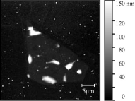
Then, halogen reactions in organic solution were investigated. Considering fluorine, chlorine and bromine are too active with photoresist and incompatible with cleanroom environment, we tested iodine solutions on BP. Considering that BP degrades when exposed to water and oxygen ambients, an organic solvent was needed Yang et al. (2018). Therefore, acetone was chosen as the solvent. After etching, 100% isopropyl alcohol (IPA) was used to rinse the samples. The samples were dried in air. As shown in Figure 1 (a) and (b), clear thinning effect were observed after a BP sample on a silicon substrate had been in a 5 g/L iodine/acetone solution for 5 minutes. The Raman spectrum in Figure 1 (c) showed good crystallinity of the sample after etching.
However, there were still problems in using acetone as the solvent, such as etching controllability, incompatibility with lithography processes, and the effects on the BP quality, which were investigated and discussed in the next section.
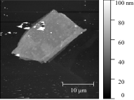
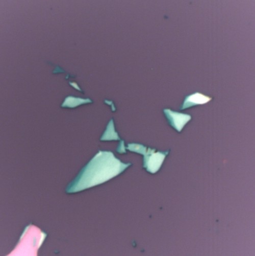
a) and b): Sample A before and after iodine/chloroform solution etching. Several large bubble-like regions with more than 100 nm height differences are damages formed during the etching.
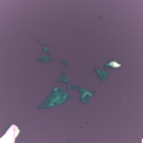
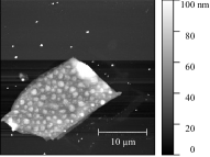
c) and d): Sample B before and after iodine/IPA-methanol solution etching. The rough surface in c) should be a result of surface oxidation during the sample preparation. Sample B after etching has a very clean and flat surface in d) when compared with those etched by chloroform solutions.


III Solvent, concentration, and time parameters for etching
III.1 Solvent dependence
A few nanofabrication-compatible organic solvents were tested to see their effects on etching process. The reaction time was 10 min and the concentration used for all solutions was 10 g/L. Acetone, chloroform and IPA-methanol mixture (IPA:methanol=1:1 in volume) solutions were observed to have an apparent thinning effect.
The iodine/acetone solution etched too fast. It completely etched the 50 nm thick sample away within 10 min. Besides, acetone could remove most kinds of positive photoresists, which makes it incompatible with photolithography process.
The iodine/chloroform solution etched the sample by 10 nm (from 20 to 10 nm in the average thickness) as shown in the Figure 2 (a) and Figure 2 (b). However, large bubble-like regions were developed during the etching process. Chloroform was believed to be the reason for BP damage due to its halogen solvent property Yasaei et al. (2015). Similar as acetone, chloroform is incompatible with common photoresists, which makes it unsuitable for photolithography.
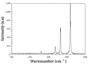
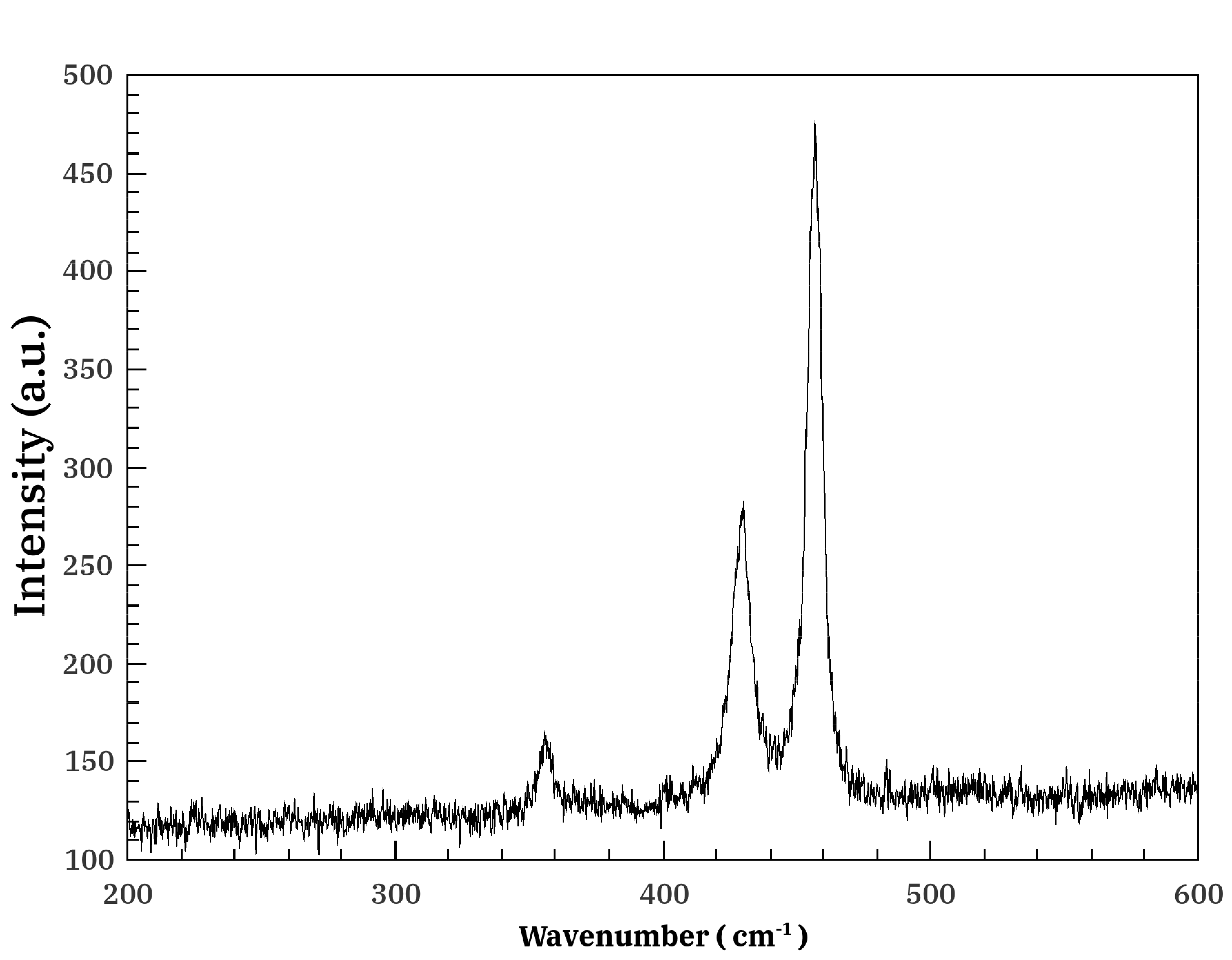
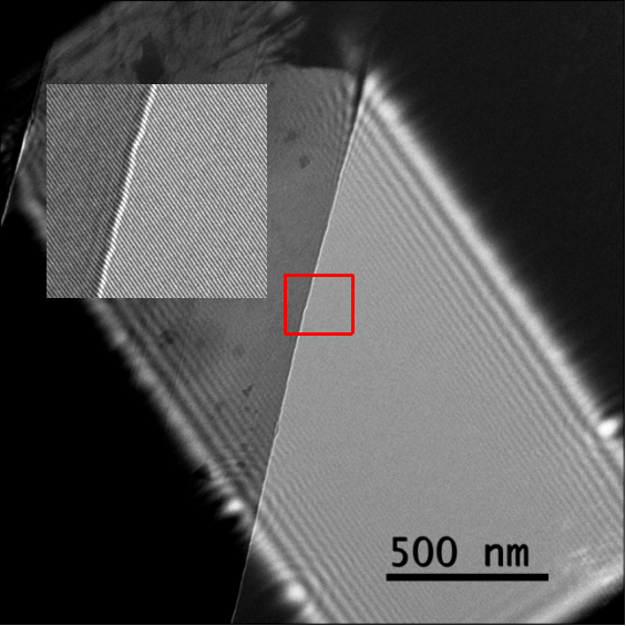
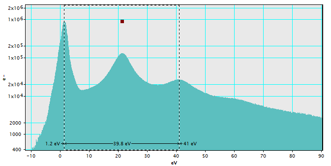
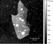
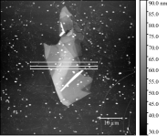
The iodine/IPA-methanol solution also etched the sample around 10 nm in 10 mins (from 50 to 40 nm) . The surface was smoother after etching as seen in Figure 2 (c) and (d). The reason was that iodine removed the oxidized BP. The etch rate was suitable for a atomic layer etching (ALE) process. To check the crystallinity and impurities, Raman spectroscopy, STEM, EDS and EELS were performed. Sample C used for STEM imaging, EDS and EELS was fabricated using an modified dry-transfer method as developed in our earlier work.Fang et al. (2018) As seen in Figure 3 (b) and (c), Raman and high resolution STEM image characterizations of Sample C confirmed that the good crystallinity remained after etching. EDS and EELS data show that Sample C was free of iodine residues after etching and rinsing.
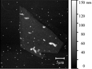
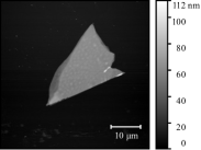
To study the etch uniformity, a sample, Sample D, was chosen, as it had a clear thickness difference and a clean surface before etching. Uniform etching along the layer-stacking direction 010 was confirmed in AFM data of Sample D as shown in Figure 4, indicating a layer-by-layer etching even when the original thickness had more than 20 nm thickness difference. The shape also remained after etching.
Therefore, an IPA-methanol mixture with a 1:1 volume ratio was found to be the most suitable solvent for BP ALE. In all the following discussions, the solutes used were iodine and the solvents used were all IPA-methanol with this volume ratio.
III.2 Time dependence
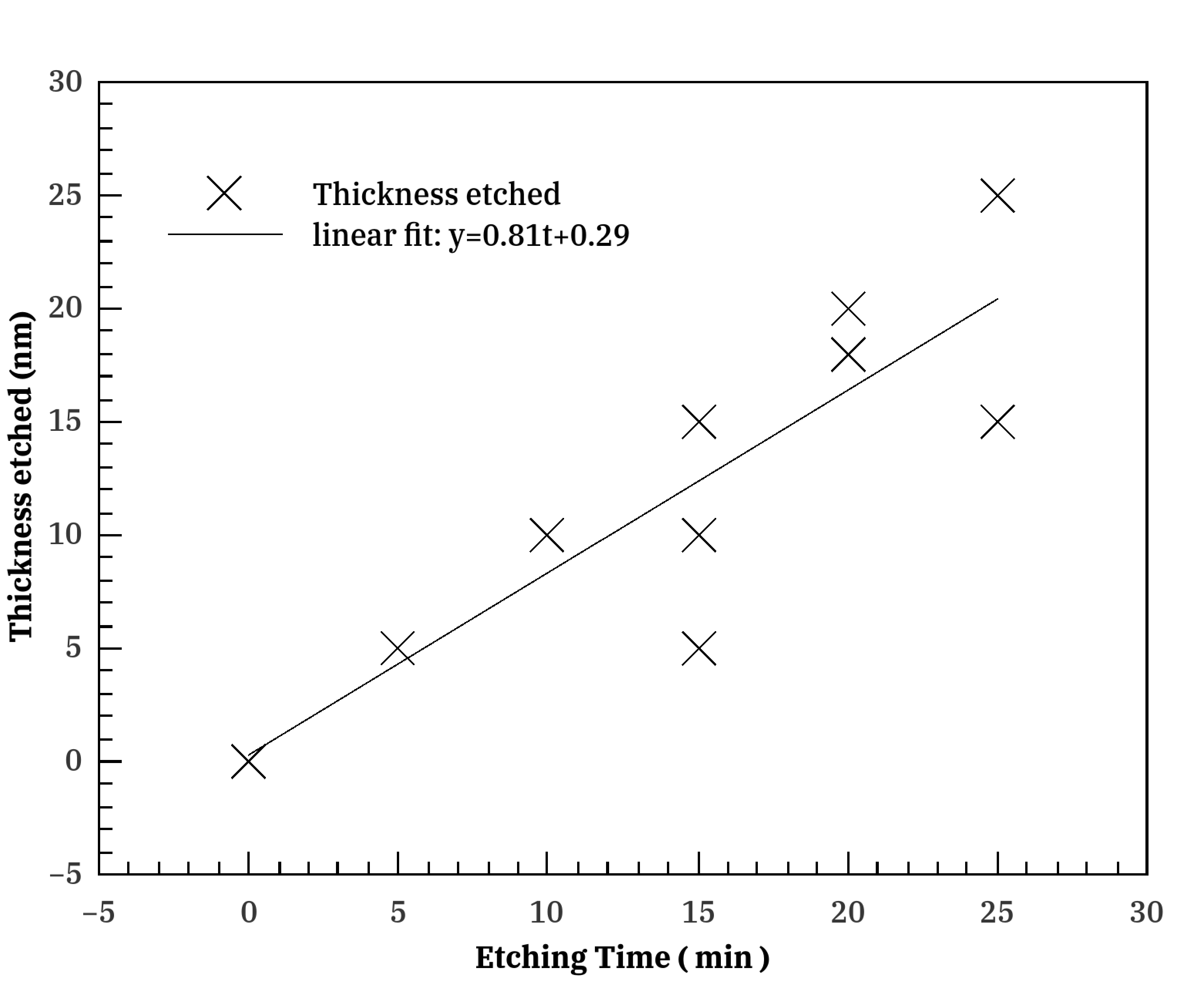
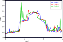
The etching thickness and time relationship under 10 g/L concentration is shown in the Figure 5. The etching thickness has a near linear dependence on time, which means that the etch rate is stable. The etch rate is 0.81 nm/min based on the linear fitting, sustainable for BP thinning control. Detailed AFM data and 1-dimensional (1D) thickness profiles are in supplementary information S3(a)-S3(j).
III.3 Concentration dependence
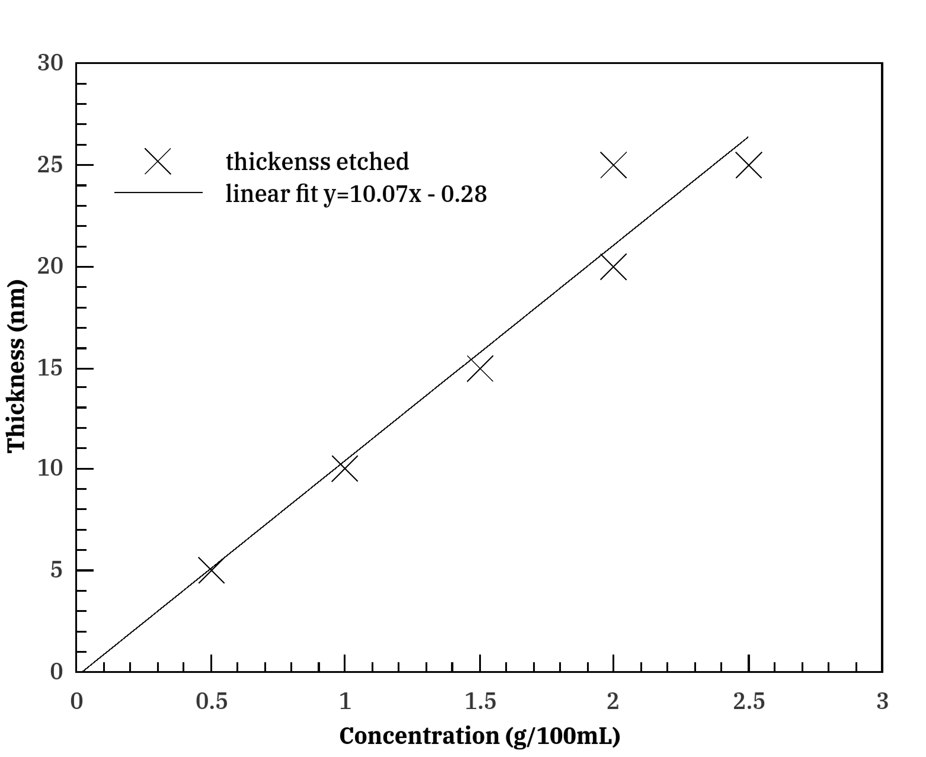
With the same etch time of 10 mins, the etching thickness and the iodine concentration relationship is shown in Figure 6. Detailed AFM data and 1-dimensional thickness profilesare shown in supplementary information S4(a)-S4(j). As the etch behavior is near linear with both the etch time and the concentration, we can express this etch behavior as 0.81-1.01 nm/(min*g/L).
IV Lithography and etching results
To obtain a thickness pattern and examine the isotropy/anisotropy of the etching method, photolithography was used. The selection of a suitable photoresist was critical for the ALE process of BP. Two major problems were encountered during our experiments: 1) IPA and methanol could dissolve most of the i-line and h-line photoresists (AZ-P series photoresists, AZ MIR 703 photoresist, S1800 series photoresists), even after long time hard baking. This greatly limited the photoresist choices; 2) BP can get damaged or oxided at high temperature, which limits the possibility of using hard masks. After some trials, PMMA(polymethyl methacrylate) photoresist was found to be friendly with IPA-methanol etching solutions, which could be used for both DUV lithography and e-beam lithography.
The lithography and ALE results were shown in Figure 7. The sample was exposed in a low-pressure mercury lamp(253nm DUV light source), developed and putted in 20 g/L iodine solution for 12 min. Then it was taken out from the etch solution when visible color change was observed on the exposed region. According to the AFM line profiles and scanning results before and after etching, we achieved around 20 nm thickness difference, which matches the etch rate we got previously. Clear vertical edge could be observed in the result with around 40:1 (nm/m) degree of anisotropy, and pattern shape accuracy is around 0.5 m. Although planar resolution for the thickness pattern is relatively low comparing with vertical resolution achieved which is atomic layer accuracy, one possible reason is that our DUV lithography condition (mask and light source as discussed in the supplementary material) limited the planar accuracy. Detailed information about our lithography facility and parameter was discussed in supplementary information (S5).

V Summary
Atomic layer accuracy BP thickness pattern was achieved using photolithography and etching method we developed. Organic solution were used as the media and environment for the etching process, made it possible to get rid of water and oxygen, which are the important sources for the defects in few layer BP. Detailed etching thickness dependence on time, concentration and solution were studied in this paper, which shown near linear dependence. PMMA was used as the photoresist in this work, which made this method compatible with DUV lithography and e-beam lithography process. Besides, this method has also shown very reliable thinning ability on BP, which could be used for large area or critically thin few-layer BP fabrication and controlling BP thickness as shown in supplementary Figure S6.
Therefore, we believe that this BP ALE process provided a low cost, high repeatability way for achieving select region BP layer number engineering which could be used for controlling BP layer number, fabricating various kind of BP quantum devices, and massively manufacturing large size, few-layer BP samples.
VI Experiment Details
VI.1 BP sample fabrication
BP samples were fabricated by mechanical exfoliation method using ScotchTM Tape. Several very thick samples(120 nm 200 nm thick) for lithography test were first thinned down to around 50 nm thick by our atomic layer etching method to fit our requirement.
VI.2 Etching solution
Etching solutions were prepared in cleanroom condition. To prevent evaporation which would affect the concentration, the etching solution was prepared only minutes before use. Ultrasonic wave were used to shorten the dissolve time.
VI.3 STEM sample preparation
STEM sample preparation was achieved by two steps. First, we use the dry transfer method designed by our group as we published earlier to transfer the BP sample and make it stiff enough on the grid. Second, we put the copper grid in the etching solution and use tweezers carefully to prevent bending or damage the grid/sample. It should be noticed that this solution also shows etching effect with the copper grid if sample was putted in the solution for more than 30min, while no visible etching effect with gold grid. So if possible we would recommend using gold grid for long time etching process.
VI.4 Lithography
PMMA photoresist was coated on the sample and spinning with 7000rpm rate. We use 1000 mesh TEM grid as the mask for DUV lithography. It should be noticed that hard baking time should be limited as BP could get oxided if it is thinner than 20 nm. Details about our DUV lithography was discussed in our supplement material.
VII Acknowledgment
We are very grateful for the kind help and suggestions on lithography from UBC cleanroom and SFU 4D lab, the EELS/EDS characterization data from Professor Kavanagh, and the AFM facility provided from UBC Centre for Flexible Electronics and Textiles and Professor Peymann for some sample’s characterization.
References
- Qiao et al. (2014) J. Qiao, X. Kong, Z.-X. Hu, F. Yang, and W. Ji, Nature Communications 5, 4475 (2014).
- Warschauer (1963) D. Warschauer, Journal of Applied Physics 34, 1853 (1963).
- Morita (1986) A. Morita, Applied Physics A 39, 227 (1986).
- Tran et al. (2014) V. Tran, R. Soklaski, Y. Liang, and L. Yang, Physical Review B 89, 235319 (2014).
- Wang et al. (2015) X. Wang, A. M. Jones, K. L. Seyler, V. Tran, Y. Jia, H. Zhao, H. Wang, L. Yang, X. Xu, and F. Xia, Nature Nanotechnology 10, 517 (2015).
- Cai et al. (2014) Y. Cai, G. Zhang, and Y.-W. Zhang, Scientific Reports 4, 6677 (2014).
- Liu et al. (2015) F. Liu, Q. Shi, J. Wang, and H. Guo, Applied Physics Letters 107, 203501 (2015), https://doi.org/10.1063/1.4935752 .
- Liu et al. (2016a) F. Liu, J. Wang, and H. Guo, in 2016 IEEE Silicon Nanoelectronics Workshop (SNW) (2016) pp. 194–195.
- Chang and Hobbs (2015) J. Chang and C. Hobbs, Applied Physics Letters 106, 083509 (2015), https://doi.org/10.1063/1.4913842 .
- Chen et al. (2017) F. W. Chen, H. Ilatikhameneh, T. A. Ameen, G. Klimeck, and R. Rahman, IEEE Electron Device Letters 38, 130 (2017).
- Klinkert et al. (2018) C. Klinkert, A. Szabo, D. Campi, C. Stieger, N. Marzari, and M. Luisier, in 2018 76th Device Research Conference (DRC) (2018) pp. 1–2.
- Li et al. (2018) H. Li, B. Shi, Y. Pan, J. Li, L. Xu, L. Xu, Z. Zhang, F. Pan, and J. Lu, Nanotechnology 29, 485202 (2018).
- Cao et al. (2015) W. Cao, J. Kang, D. Sarkar, W. Liu, and K. Banerjee, IEEE Transactions on Electron Devices 62, 3459 (2015).
- Meng et al. (2018) Z. Meng, J. Zhuang, X. Xu, W. Hao, S. X. Dou, and Y. Du, Advanced Materials Interfaces 5, 1800749 (2018), https://onlinelibrary.wiley.com/doi/pdf/10.1002/admi.201800749 .
- Cao and Guo (2015) X. Cao and J. Guo, IEEE Transactions on Electron Devices 62, 659 (2015).
- Zeng et al. (2014) Q. Zeng, H. Wang, W. Fu, Y. Gong, W. Zhou, P. M. Ajayan, J. Lou, and Z. Liu, Small 11, 1868 (2014), https://onlinelibrary.wiley.com/doi/pdf/10.1002/smll.201402380 .
- Li et al. (2014) L. Li, Y. Yu, G. J. Ye, Q. Ge, X. Ou, H. Wu, D. Feng, X. H. Chen, and Y. Zhang, Nature Nanotechnology 9, 372 (2014).
- Castellanos-Gomez et al. (2014) A. Castellanos-Gomez, L. Vicarelli, E. Prada, J. O. Island, K. L. Narasimha-Acharya, S. I. Blanter, D. J. Groenendijk, M. Buscema, G. A. Steele, J. V. Alvarez, H. W. Zandbergen, J. J. Palacios, and H. S. J. van der Zant, 2D Materials 1, 025001 (2014).
- Liu et al. (2016b) X. Liu, K.-S. Chen, S. A. Wells, I. Balla, J. Zhu, J. D. Wood, and M. C. Hersam, Advanced Materials 29, 1604121 (2016b), https://onlinelibrary.wiley.com/doi/pdf/10.1002/adma.201604121 .
- Hanlon et al. (2015) D. Hanlon, C. Backes, E. Doherty, C. S. Cucinotta, N. C. Berner, C. Boland, K. Lee, A. Harvey, P. Lynch, Z. Gholamvand, S. Zhang, K. Wang, G. Moynihan, A. Pokle, Q. M. Ramasse, N. McEvoy, W. J. Blau, J. Wang, G. Abellan, F. Hauke, A. Hirsch, S. Sanvito, D. D. O’Regan, G. S. Duesberg, V. Nicolosi, and J. N. Coleman, Nature Communications 6, 8563 (2015).
- Yasaei et al. (2015) P. Yasaei, B. Kumar, T. Foroozan, C. Wang, M. Asadi, D. Tuschel, J. E. Indacochea, R. F. Klie, and A. Salehi-Khojin, Advanced Materials 27, 1887 (2015).
- Lewis et al. (2017) E. A. Lewis, J. R. Brent, B. Derby, S. J. Haigh, and D. J. Lewis, Chemical Communication 53, 1445 (2017).
- Ambrosi et al. (2017) A. Ambrosi, Z. Sofer, and M. Pumera, Angewandte Chemie International Edition 56, 10443 (2017).
- Yang et al. (2018) S. Yang, K. Zhang, A. G. Ricciardulli, P. Zhang, Z. Liao, M. R. Lohe, E. Zschech, P. W. M. Blom, W. Pisula, K. Müllen, and X. Feng, Angewandte Chemie 130, 4767 (2018).
- Robbins et al. (2017) M. C. Robbins, S. Namgung, S.-H. Oh, and S. J. Koester, ACS Applied Materials & Interfaces 9, 12654 (2017), pMID: 28286947, https://doi.org/10.1021/acsami.6b14477 .
- Fan et al. (2017) S. Fan, H. Hei, C. An, W. Pang, D. Zhang, X. Hu, S. Wu, and J. Liu, Journal of Materials Chemistry C 5, 10638 (2017).
- Lin et al. (2017) S. Lin, Y. Li, W. Lu, Y. S. Chui, L. Rogée, Q. Bao, and S. P. Lau, 2D Materials 4, 025001 (2017).
- Luo et al. (2017) W. Luo, R. Yang, J. Liu, Y. Zhao, W. Zhu, and G. M. Xia, Nanotechnology 28, 285301 (2017).
- Park et al. (2017) J. W. Park, S. K. Jang, D. H. Kang, D. S. Kim, M. H. Jeon, W. O. Lee, K. S. Kim, S. J. Lee, J.-H. Park, K. N. Kim, and G. Y. Yeom, Journal of Materials Chemistry C 5, 10888 (2017).
- Venugopalan and Mathai (1956) M. Venugopalan and K. U. Mathai, Fresenius’ Zeitschrift für analytische Chemie 151, 262 (1956).
- Yoza and Ohashi (1965) N. Yoza and S. Ohashi, BCSJ 38, 1408 (1965).
- Rosenstein (1920) L. Rosenstein, Journal of the American Chemical Society 42, 883 (1920).
- Walker (1926) O. J. Walker, Journal of the Chemical Society 129, 1370 (1926).
- BECKER and SCHEER (1995) U. BECKER and M. SCHEER, Abstracts of Papers of the American Chemical Society 209, 118 (1995).
- Han et al. (2000) C. Han, X. Zhao, X. Zhang, Z. Gao, and Q. Zhu, Rapid Commun. Mass Spectrom. 14, 1255 (2000).
- Venugopalan and George (1957) M. Venugopalan and K. George, Bulletin of the Chemical Society of Japan 30, 51 (1957).
- de Largy et al. (1983) B. de Largy, A. Finch, P. J. Gardner, and N. Kell, Journal of the Chemical Society, Faraday Trans. 1 79, 383 (1983).
- DORFMAN et al. (1994) Y. A. DORFMAN, M. M. ALESHKOVA, and F. K. FAISOVA, Zhurnal Obshchei Khimii 64, 1462 (1994).
- Gusarova et al. (1989) N. K. Gusarova, B. A. Trofimov, S. F. Malysheva, T. N. Rakhmatulina, E. P. Vyalykh, and M. G. Voronkov, Bulletin of the Academy of Sciences of the USSR, Division of chemical science 38, 430 (1989).
- Potapov et al. (1989) V. A. Potapov, S. V. Amosova, and A. V. Khangurov, Bulletin of the Academy of Sciences of the USSR, Division of chemical science 38, 195 (1989).
- Badeeva et al. (2003) E. K. Badeeva, S. S. Krokhina, and B. E. Ivanov, Russian Journal of General Chemistry 73, 1376 (2003).
- Kuimov et al. (2011) V. A. Kuimov, S. F. Malysheva, N. K. Gusarova, T. I. Vakul’skaya, S. S. Khutsishvili, and B. A. Trofimov, Heteroatom Chemistry 22, 198 (2011).
- Malysheva et al. (2012) S. F. Malysheva, A. V. Artem’ev, N. A. Belogorlova, A. O. Korocheva, N. K. Gusarova, and B. A. Trofimov, Russian Journal of General Chemistry 82, 1307 (2012).
- Gusarova et al. (2001) N. K. Gusarova, Y. V. Smetannikov, B. G. Sukhov, S. F. Malysheva, N. P. Tarasova, and B. A. Trofimov, Russian Journal of General Chemistry 71, 643 (2001).
- Trofimov et al. (2008) B. A. Trofimov, S. I. Verkhoturova, V. L. Mikhailenko, T. I. Kazantseva, S. N. Arbuzova, A. A. Tatarinova, L. V. Klyba, and N. K. Gusarova, Russian Journal of General Chemistry 78, 1816 (2008).
- Fang et al. (2018) T. Fang, T. Liu, Z. Jiang, R. Yang, P. Servati, and G. M. Xia, arXiv preprint arXiv:1805.01135 (2018).