Present address: ]Centre de Nanosciences et de Nanotechnologies (C2N), CNRS, Univ Paris Sud, Université Paris-Saclay, 91120 Palaiseau, France ††thanks: S.Ch. and R. R.-P. contributed equally to this work
High quality electrostatically defined hall bars in monolayer graphene
Realizing graphene’s promise as an atomically thin and tunable platform for fundamental studies and future applications in quantum transport requires the ability to electrostatically define the geometry of the structure and control the carrier concentration, without compromising the quality of the system. Here, we demonstrate the working principle of a new generation of high quality gate defined graphene samples, where the challenge of doing so in a gapless semiconductor is overcome by using the insulating state, which emerges at modest applied magnetic fields. In order to verify that the quality of our devices is not compromised by the presence of multiple gates we compare the electronic transport response of different sample geometries, paying close attention to fragile quantum states, such as the fractional quantum Hall (FQH) states, that are highly susceptible to disorder. The ability to define local depletion regions without compromising device quality establishes a new approach towards structuring graphene-based quantum transport devices.
An important feature of two-dimensional (2D) electron systems is the ability to vary the charge carrier density by electrostatic gating. In semiconductor heterostructures this allows the geometry of the conducting region to be dynamically modified by using patterned gates to define local depletion regions. As a result, a variety of tunable device structures can be realized that allow the study and manipulation of 2D quantum transport phenomenon, ranging for example from single quantum point contactsvan Houten and Beenakker (1996) to complex multi-terminal devices such as edge state interferometersvan Wees et al. (1989); de C. Chamon et al. (1997). The recently developed graphene-based devices provide in principle a versatile new platform for the development of a new generation of quantum transport devices. The high quality of these samples is reflected by a carrier mobility which compares to the theoretical limit imposed by acoustic phonon scattering and a mean free path that can exceed the sample size Wang et al. (2013), while the linear bandstructure and expanded degrees of freedom offer new capabilities beyond conventional systemsCastro Neto et al. (2009). However, because monolayer graphene is gapless, it cannot be rendered insulating simply by depleting the region under the electrostatic gates. While device structures can be shaped by lithographic patterning and etching, the resulting geometries are not tunable, and their response is typically dominated by the resulting edge disorderBischoff et al. (2015). Previous attempts to electrostatically define a channel in monolayer graphene, in the quantum Hall regime, lacked of an insulating state, complicating the control on edge states and understanding of the system Wei et al. (2017); Zimmermann et al. (2017); Kim et al. (2016); Nakaharai et al. (2011).
Here we demonstrate the working principle of a new generation of high–quality gate–defined monolayer graphene devices where an insulating state underneath the gate is achieved using the properties of graphene under magnetic field. To confirm the high quality of our samples we compare the electronic transport response of fragile quantum states, such as the fractional quantum Hall effect (FQHE) states, in different sample geometries. These states are used as sensitive indicators of quality. In a conventional 2D electron gas (2DEG) the use of electrostatic gates to change the carrier density and/or to define electrostatically is generally found to compromise the quality of the 2DEG Pan et al. (2017); Bachsoliani et al. (2017). We observe a similar result in graphene when using evaporated metal gates but find that exfoliated graphite gates allows us to maintain high mobility.
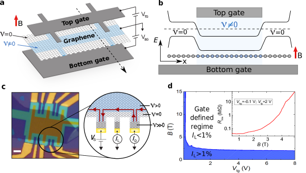
Fig. 1a-c illustrates the working principle in our devices. In a sufficiently large perpendicular magnetic field the N=0 Landau level (LL) in graphene splits into sub-levels with an antiferromagnetic state appearing at that is characterized by being gapped both in the bulk and at the edgesYoung et al. (2012, 2014); Bolotin et al. (2009); Amet et al. (2014). Using the bottom gate we tune the entire device into this state. We then apply a finite bias to a patterned top gate, defining the active region. Both the top and bottom gate are separated from the graphene channel by multi-layer hexagonal boron nitride (BN) (not shown in Fig. 1a). To fabricate these devices we assemble the heterostructure using the van der Waals assembly techniqueWang et al. (2013). We then use two successive etching steps first to shape the entire structure into a multi-terminal Hall bar, then a second etch to further shape the top gate to a smaller Hall bar. An optical image of the final device is shown in Fig. 1c. A portion of the graphene leads extends past the bottom graphite gate before making contact with the evaporated edge-contactWang et al. (2013). In all of the measurements presented here the carrier density of this extended lead region is tuned to high density (using the Si bottom gate) to ensure good electrical contact in the QHE regimeMaher et al. (2014) (see supplementary information).
In order to confirm the insulating behaviour in the single-gated depletion regions, the devices also incorporate extra leads (thinner electrodes seen in Fig. 1c) that are used to measure any leakage current (Fig. 1d) through the insulating region. As a benchmark we consider the device to be in the gate defined regime whenever the leakage current measures less than % of the total current flowing through the device. The combination of magnetic field and gate voltage required to achieve this state is shown by the white area in Fig. 1d. An almost exponential increase of the resistance of the insulating state as a function of the magnetic field can be observed in the insert of Fig. 1d.
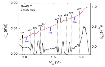
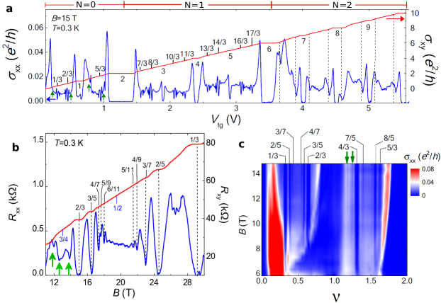
Fig. 2a shows the longitudinal () and Hall () conductivity at T as a function of the top-gate voltage for a device operated in the gate defined regime. The result shows very high quality transport response with a large number of FQHE states observable in the first two LLs (N=0 and N=1). In addition, onset of multiples of states can be observed in the longitudinal conductivity for the N=2 LL. Similarly to the fractional states previously reported in the third LL of ultra-high mobility GaAs/AlGaAs samples Gervais et al. (2004). Figure 2b shows the longitudinal and Hall resistance for the N=0 LL versus magnetic field measured up to T. In addition to the sequence of two-flux composite fermion (CF) statesJain (2007) around , we observe the presence of four-flux CF states around . These 4CF states have previously only been observed in local electronic compressibility measurements in suspended graphene Feldman et al. (2013, 2012).
Fig. 2c shows evolution of the FQHE states with magnetic field. The strongest states persist to less than 6 T. This is among the lowest fields at which transport signatures of the FQHE have been observed in graphene Hall bars, further confirming the high quality of our deviceAmet et al. (2015).
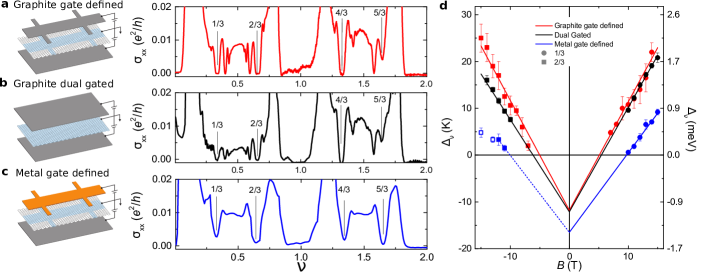
In our device structure the active region is fully encapsulated in graphite gates, which is a geometry that previously has been shown to significantly improve transport response. In an effort to understand what role this plays in our device response we compare measurements from three device geometries, where in all cases we maintain a global bottom graphite gate, and vary details of the top gate. The structures we considered (illustrated in Fig. 3a-c) include (i) a patterned graphite top gate (as described above) operated in the gate-defined regime, (ii) a global graphite top gate in which the device edges are defined by lithographic etching and (iii) a similar gate-defined device as in (i), but with an evaporated metal forming the top gate.
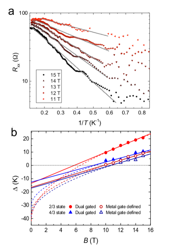
We first observe that, compared to the metal-gated structure, both of the graphite-gated devices show a larger number of well developed FQH states. This suggests that the use of a graphite gate is playing a role in improving the quality of the device and that, as in the case of conventional 2DEGs, the use of metal gates adversely affects device quality. A more quantitative comparison among the devices of Fig. 3a-c is provided by measuring the magnetic field dependence of the energy gaps of the FQH states, (Fig. 3d). These energy gaps are extracted by thermal activation measurements, , where is Boltzmann’s constant. We assume that the 1/3 and 2/3 FQH gaps, which follow approximately linear in B dependence, correspond to the CF Zeeman energy , where is the Bohr magneton and is the Landé g-factor Dethlefsen et al. (2006); Zeng et al. (2018); Schulze-Wischeler et al. (2004). The intercept of this linear fit, gives the broadening of the CF Landau levels (or -levels), , providing a quantitative comparison of sample disorder. The value of for the graphite gate defined and dual graphite gated devices is almost identical K, and also in excellent agreement with recent corbino measurements Zeng et al. (2018). We note that the two graphite gated devices fabricated from the same heterostructure however a similar response was found in another similarly constructed sample (see SI). In contrast, the metal gate-defined device clearly shows a larger than the two graphite-gated devices. This suggests that the use of two graphite gates results in a lower bulk disorder compared with evaporated metal gates, consistent with other recent studies Zibrov et al. (2016). The origin of the increased disorder in devices with metal gates remains to be explored.
High quality FQHE in graphene at lower magnetic fields is an important achievement by itself since it enables the study of CF in a more tunable material. For example, using the same analysis we also extracted a Landé g-factor ranging between 6.9 and 4.9, which suggests strong electronic interaction and possible spin textures, already proposed to exist in grapheneZeng et al. (2018); Dean et al. (2011). Additionally, these enhanced electronic interactions in our sample are observed by the presence of a reentrant integer quantum Hall effect (RIQHE) at higher magnetic fields, as reported in Chen et al. (2019).
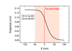
Finally we consider the nature of the QHE edge state in these gate defined Hall bars. Due to the close proximity and sharp termination of the patterned graphite gate, the confinement potential may be substantially different from bottom-gated devices with etched boundariesCui et al. (2016); Weis2011. In the gate defined and dual gated cases we expect the new electrostatic profile to be soft (varying over 60 nm for our devices, see supplementary information). A broader confinement will be reflected in a larger spacial separation between edge states which could have a significant impact on details of the FQHE edge transportGrivnin et al. (2014). While detailed consideration of these effects is beyond the present work, the ability to modify the electrostatic profiles by choice of BN dielectric thickness provides an opportunity explore these effects in future experiments.
To summarize, we demonstrate that electrostatic gating can be used to define the geometry of graphene devices by utilizing the gap of the quantum Hall effect to maintain an insulating state. Whereas metal gates introduce disorder, graphite gates are compatible with ultrahigh-quality devices, as assessed by measurement of FQH response and observation of electron solid states through observation of RIQHE. The ability to define local depletion regions without compromising device quality establishes a new approach towards structuring graphene-based quantum transport devices. In particular our results establish the capability to combine robust FQHE states with complex structures in graphene such as quantum point contacts and edge state interferometers. These are the essential pieces for the possible study of fractional and non-Abelian statistics.
References
- van Houten and Beenakker (1996) H. van Houten and C. Beenakker, Physics Today 49, 22 (1996).
- van Wees et al. (1989) B. J. van Wees, L. P. Kouwenhoven, C. J. P. M. Harmans, J. G. Williamson, C. E. Timmering, M. E. I. Broekaart, C. T. Foxon, and J. J. Harris, Phys. Rev. Lett. 62, 2523 (1989).
- de C. Chamon et al. (1997) C. de C. Chamon, D. E. Freed, S. A. Kivelson, S. L. Sondhi, and X. G. Wen, Phys. Rev. B 55, 2331 (1997).
- Wang et al. (2013) L. Wang, I. Meric, P. Y. Huang, Q. Gao, Y. Gao, H. Tran, T. Taniguchi, K. Watanabe, L. M. Campos, D. A. Muller, J. Guo, P. Kim, J. Hone, K. L. Shepard, and C. R. Dean, Science 342, 614 (2013).
- Castro Neto et al. (2009) A. H. Castro Neto, F. Guinea, N. M. R. Peres, K. S. Novoselov, and A. K. Geim, Rev. Mod. Phys. 81, 109 (2009).
- Bischoff et al. (2015) D. Bischoff, A. Varlet, P. Simonet, M. Eich, H. C. Overweg, T. Ihn, and K. Ensslin, Applied Physics Reviews 2, 031301 (2015).
- Wei et al. (2017) D. S. Wei, T. van der Sar, J. D. Sanchez-Yamagishi, K. Watanabe, T. Taniguchi, P. Jarillo-Herrero, B. I. Halperin, and A. Yacoby, Science Advances , arXiv:1703.00110 (2017).
- Zimmermann et al. (2017) K. Zimmermann, A. Jordan, F. Gay, K. Watanabe, T. Taniguchi, Z. Han, V. Bouchiat, H. Sellier, and B. Sacépé, Nature Communications 8, 14983 EP (2017).
- Kim et al. (2016) M. Kim, J.-H. Choi, S.-H. Lee, K. Watanabe, T. Taniguchi, S.-H. Jhi, and H.-J. Lee, Nat Phys 12, 1022 (2016).
- Nakaharai et al. (2011) S. Nakaharai, J. R. Williams, and C. M. Marcus, Phys. Rev. Lett. 107, 036602 (2011).
- Pan et al. (2017) W. Pan, W. Kang, K. W. Baldwin, K. W. West, L. N. Pfeiffer, and D. C. Tsui, Nature Physics , EP (2017).
- Bachsoliani et al. (2017) N. Bachsoliani, S. Platonov, A. Wieck, and S. Ludwig, ArXiv , 1708.02034 (2017).
- Young et al. (2012) A. F. Young, C. R. Dean, L. Wang, H. Ren, P. Cadden-Zimansky, K. Watanabe, T. Taniguchi, J. Hone, K. L. Shepard, and P. Kim, Nat Phys 8, 550 (2012).
- Young et al. (2014) A. F. Young, J. D. Sanchez-Yamagishi, B. Hunt, S. H. Choi, K. Watanabe, T. Taniguchi, R. C. Ashoori, and P. Jarillo-Herrero, Nature 505, 528 (2014).
- Bolotin et al. (2009) K. I. Bolotin, F. Ghahari, M. D. Shulman, H. L. Stormer, and P. Kim, Nature 462, 196 (2009).
- Amet et al. (2014) F. Amet, J. R. Williams, K. Watanabe, T. Taniguchi, and D. Goldhaber-Gordon, Phys. Rev. Lett. 112, 196601 (2014).
- Maher et al. (2014) P. Maher, L. Wang, Y. Gao, C. Forsythe, T. Taniguchi, K. Watanabe, D. Abanin, Z. Papić, P. Cadden-Zimansky, J. Hone, P. Kim, and C. R. Dean, Science 345, 61 (2014).
- Gervais et al. (2004) G. Gervais, L. W. Engel, H. L. Stormer, D. C. Tsui, K. W. Baldwin, K. W. West, and L. N. Pfeiffer, Phys. Rev. Lett. 93, 266804 (2004).
- Jain (2007) J. K. Jain, Composite Fermions (Cambridge University Press, 2007).
- Feldman et al. (2013) B. E. Feldman, A. J. Levin, B. Krauss, D. A. Abanin, B. I. Halperin, J. H. Smet, and A. Yacoby, Phys. Rev. Lett. 111, 076802 (2013).
- Feldman et al. (2012) B. E. Feldman, B. Krauss, J. H. Smet, and A. Yacoby, Science 337, 1196 (2012).
- Amet et al. (2015) F. Amet, A. J. Bestwick, J. R. Williams, L. Balicas, K. Watanabe, T. Taniguchi, and D. Goldhaber-Gordon, Nat Commun 6 (2015).
- Dethlefsen et al. (2006) A. F. Dethlefsen, E. Mariani, H.-P. Tranitz, W. Wegscheider, and R. J. Haug, Phys. Rev. B 74, 165325 (2006).
- Zeng et al. (2018) Y. Zeng, J. I. A. Li, S. A. Dietrich, O. M. Ghosh, K. Watanabe, T. Taniguchi, J. Hone, and C. R. Dean, arXiv (2018), 1805.04904 .
- Schulze-Wischeler et al. (2004) F. Schulze-Wischeler, E. Mariani, F. Hohls, and R. J. Haug, Phys. Rev. Lett. 92, 156401 (2004).
- Zibrov et al. (2016) A. A. Zibrov, C. R. Kometter, T. Taniguchi, K. Watanabe, M. P. Zaletel, and A. F. Young, arXiv: , 1611.07113v1 (2016).
- Dean et al. (2011) C. R. Dean, A. F. Young, P. Cadden-Zimansky, L. Wang, H. Ren, K. Watanabe, T. Taniguchi, P. Kim, J. Hone, and K. L. Shepard, Nat Phys 7, 693 (2011).
- Chen et al. (2019) S. Chen, R. Ribeiro-Palau, K. Yang, K. Watanabe, T. Taniguchi, J. Hone, M. O. Goerbig, and C. R. Dean, Phys. Rev. Lett. 122, 026802 (2019).
- Cui et al. (2016) Y.-T. Cui, B. Wen, E. Y. Ma, G. Diankov, Z. Han, F. Amet, T. Taniguchi, K. Watanabe, D. Goldhaber-Gordon, C. R. Dean, and Z.-X. Shen, Phys. Rev. Lett. 117, 186601 (2016).
- Grivnin et al. (2014) A. Grivnin, H. Inoue, Y. Ronen, Y. Baum, M. Heiblum, V. Umansky, and D. Mahalu, Phys. Rev. Lett. 113, 266803 (2014).
Acknowledgements
We acknowledge discussions with M. O. Goerbig. S. Chen is supported by the ARO under MURI W911NF-17-1-0323. This research was supported by the NSF MRSEC programme through Columbia in the Center for Precision Assembly of Superstratic and Superatomic Solids (DMR-1420634). A portion of this work was performed at the National High Magnetic Field Laboratory, which is supported by National Science Foundation Cooperative Agreement No. DMR-1157490 and the State of Florida.
Author Contributions
R.R.-P., S.C. and C.R.D. designed the experiment. S.C. and Y.Z. fabricated the samples. R.R.-P. and S.C performed the experiments, analyzed the data and wrote the paper. T.T. and K.W. grew the crystals of hexagonal boron nitride. J.H. and C.R.D. advised on experiments, data analysis and writing the paper.
Supplementary Information
I Si gated contacts
Electrical contacts play an important role in device performance. As explained in the main text, in our devices a portion of the graphene leads extends out of the graphite bottom local gate. This region is used as a tunable electrical contact controlled by the global Si back gate, see Fig. S1a. In all our experiments the Si gate is set inside a high index Landau level (corresponding to a V) since the separation between LL decreases as the doping increases making easier to keep the graphene at the leads in a metallic state.
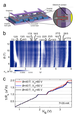
Effects of an inadequate doping of the contacts can be seen for example in the 2D map of filling factor versus magnetic field of a graphite gate-defined device, as the one presented in Fig. S1b. In this, the horizontal white areas, which correspond to an artificial increase of the longitudinal conductivity, are an effect of the LLs developing at the contacts as evidence by their periodicity in 1/. In Fig. S1c we can also see the impact of changing the Fermi energy of the contacts. As the Fermi energy of the Si gated contacts is moved from the inside of a LL it passes from a metallic to a quantum Hall regime where the edge states of the Hall bar and those developed at the contact will interact generating a deviation from the quantized values.
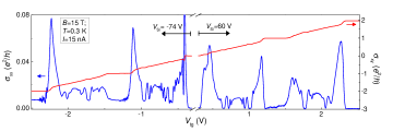
Using these doped graphene contacts it is necessary to change the nature of the doping carriers by inverting the polarity of the Si gate voltage in order to access the hole regimen, Fig. S2. It is important to mention that even when the hole doped regime can be access this one shows a lower quality than the electron doped regime.
II Gate-defined devices characterization
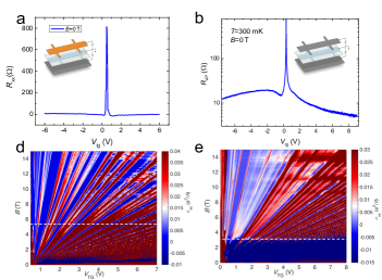
The zero field response of the three devices show in Fig. S3a-c was taken with the bottom gate at the CNP and sweeping the top gate. None of these devices show characteristics of BN/graphene alignment: satellite peaks or insulating state at the CNP. The extracted mobilities are all cm2V-1s-1.
In Fig. S3d-f the gate and magnetic field sweep for two devices, from these we can see that the magnetic field at which gate-defined regime achieved, as expected, also dependent on the sample disorder. In the main text we show that the metal gate defined posses a larger bulk disorder, this can also be seen in the need of a larger magnetic field to achieve the gate-defined regime or in other words to fully open the gap.
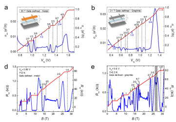
In Fig. S4 we present some extra measurements of these devices which shows the enhanced FQHE in the graphite gate-defined.
III Effects of the insulating state
The state is a exchange-enhanced energy gap where the bulk and edges of the sample are gapped. In Fig. S5 we present the magnetic field dependence of the insulating state at low temperature. This plot shows that the insulating state appear at rather low magnetic field and extend all the way to high magnetic fields. As we increase the magnetic field the voltage range of this gap is enlarged proving that our measurements are not jeopardize by a gap closing and it is not limited to a short range of bottom gate voltage.
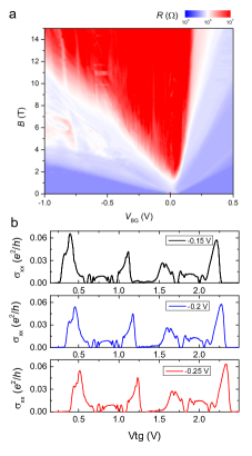
In our measurements different values of the bottom gate voltage do not affect the FQH response. We can see in Fig. S5b that the FQH response of this graphite gate-defined sample is not affected by the voltage value of the bottom gate as long as it is in the insulating regime.
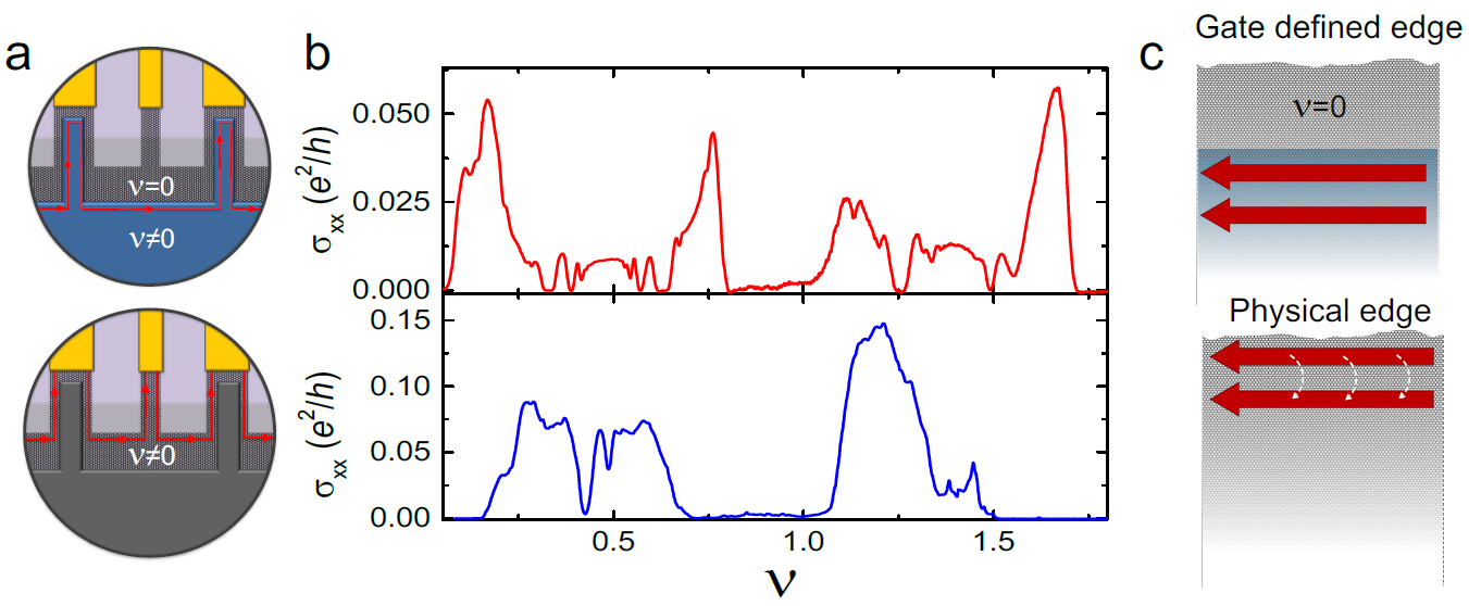
If the sample is not in the gate defined regime a mix of states occurs and the quantization of states is jeopardize. In the extreme case where the to gate is set to 0 V and the back gate changes the whole Fermi energy of the system the edge states will circulate on the crystal edge, Fig. SS6a, we can see that the number of FQH states is highly reduced. In the case where the edge states circulate on the physical edge of the sample the in-homogeneous electrostatic landscape destroys the signature of the FQHE.
