Atomistic defect states as quantum emitters in monolayer MoS2
Abstract
Quantum light sources in solid-state systems are of major interest as a basic ingredient for integrated quantum device technologies. The ability to tailor quantum emission through deterministic defect engineering is of growing importance for realizing scalable quantum architectures. However, a major difficulty is that defects need to be positioned site-selectively within the solid. Here, we overcome this challenge by controllably irradiating single-layer MoS2 using a sub-nm focused helium ion beam to deterministically create defects. Subsequent encapsulation of the ion bombarded MoS2 flake with high-quality hBN reveals spectrally narrow emission lines that produce photons at optical wavelengths in an energy window of one to two hundred below the neutral 2D exciton of MoS2. Based on ab-initio calculations we interpret these emission lines as stemming from the recombination of highly localized electron-hole complexes at defect states generated by the helium ion bombardment. Our approach to deterministically write optically active defect states in a single transition metal dichalcogenide layer provides a platform for realizing exotic many-body systems, including coupled single-photon sources and exotic Hubbard systems.
I Introduction
Point defects are important for a variety of physical phenonema in semiconductors. For example, they provide a means to engineer the equilibrium free-carrier density, they can serve as quantum emitters, and may realize quantum bits for quantum information processors.Aharonovich et al. (2016) A major challenge in several of these applications is that the defects need to be precisely positioned, which is particularly challenging for conventional three-dimensional semiconductors where defects are often buried deep in the bulk structure. A step to remedy this challenge is to reduce the physical dimension. Over the last decade it became possible to fabricate and manipulate atomically thin two-dimensional (2D) materials that offer intriguing electronic and optoelectronic properties.Ajayan et al. (2016); Roldán et al. (2017) In particular, the hexagonal transition metal dichalcogenides (TMDCs) such as MoS2, MoSe2, WS2, and WSe2 are excellent candidates for photonic applications due to their exceptionally strong light-matter interaction resulting from weak non-local dielectric screening.Mak et al. (2010); Splendiani et al. (2010); Florian et al. (2018) The strong Coulomb coupling manifests itself in an exciton dominated spectral response and very large exciton binding energies.Mak et al. (2010); Splendiani et al. (2010); Ugeda et al. (2014); Chernikov et al. (2014); He et al. (2014)
Beyond the response of mobile excitons, also quantum dot-like emission from localized excitons was recently demonstrated in WSe2,Tonndorf et al. (2015); Srivastava et al. (2015); He et al. (2015); Koperski et al. (2015); Chakraborty et al. (2015) GaSe,Tonndorf et al. (2017) MoSe2Branny et al. (2016) and WS2Palacios-Berraquero et al. (2017) and the nature of the potential which localizes the excitons is not yet fully understood. The origin of such quantum emitters is hitherto considered to be caused by uncontrolled strain potentials that locally reduce the bandgap, thus, funneling the recombination of excitons via a discrete recombination center.Kern et al. (2016); Branny et al. (2017); Palacios-Berraquero et al. (2017); Blauth et al. (2018) However, strain potentials are challenging to control, which limits the applicability of such quantum emitters for a prospective integration into photonic circuits. Laucht et al. (2012); Reithmaier et al. (2015); Goodfellow et al. (2014, 2015); Blauth et al. (2017, 2018) In particular, scalable quantum technologies require the development of controlled approaches for the direct site-selective planar integration of quantum emitters with atomic scale resolution.
In this work, we propose and investigate an alternative route to engineer single defect emitters that are of atomic scale. Specifically, we demonstrate theoretically and experimentally that localized defects in two-dimensional layers create trapping potentials in which bound complexes are formed that emit in a range of about hundred meV below the free exciton line in MoS2. Our experimental approach to systematically create such point defects is by helium ion bombardment of atomically thin MoS2. Compared to strain engineering, a controlled bombardment with helium ions is superior due to the sub-nm beam size that is perfectly suited to structure 2D materials at the nanometer scale. Fox et al. (2015) First attempts to generate optically active defects in TMDCs have been made by bombarding the host crystal with -particles Tongay et al. (2013) and helium ions.Klein et al. (2017) However, in these works a strong dynamical inhomogeneous linewidth broadening of was imposed on the emission due to the fluctuating environment. Here, we demonstrate that the encapsulation of helium irradiated MoS2 monolayers with hBN allows one to define single defect emitters with very narrow linewidths. The combination of ion-bombardment and subsequent encapsulation results in a hitherto unobserved new class of spatially localized and spectrally narrow defect emission in MoS2 at very distinct energies on the order of below the neutral exciton . Our spectroscopic observations are consistent with quantum emission that stems from defect centers in MoS2, which serve as highly-localized exciton emission centers. The interpretation is corroborrated by analyzing in detail the lineshape of the new emission peaks. This allows us to determine the interaction of the localized exciton with phonons which indicates that the emitters are localized on a nanometer scale. Our study paves the way for inducing highly controllable single defect emitters in two-dimensional materials to create arrays of coupled single-photon sources,Aharonovich et al. (2016) to study Anderson’s orthogonality catastrophe,Anderson (1967); Schmidt et al. (2018) and to realize lattices of excitons similarly to optical lattices for ultracold atomic gases.Bloch et al. (2008)
II Results
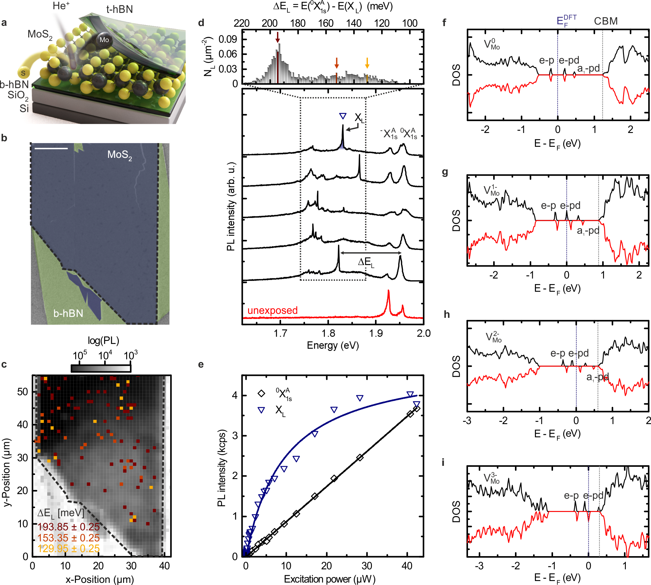
The van der Waals heterostrutures studied in this work are iteratively stacked onto Si substrates covered with thermally grown SiO2, followed by multilayered hBN, and a single layer of MoS2. Typical hBN thicknesses vary between as confirmed by atomic force microscopy. The samples are transferred into a helium ion microscope, and are locally exposed to helium ions at a constant dose of , see Figure 1a. Figure 1b shows a helium-ion microscope (HIM) image of the bombarded van der Waals heterostructure. After the ion bombardment, the entire MoS2 crystal is fully encapsulated by another multilayer hBN capping.
We perform low-temperature -photoluminescence (-PL) spectroscopy on the samples kept in a helium flow cryostat at a lattice temperature of 10 K. For excitation, we use a cw laser with a photon energy of and a low excitation power (excitation power density) of less than (). Figure 1c shows the spatially resolved and spectrally integrated -PL response as a false color representation. Representative luminescence spectra from five randomly selected positions of the exposed sample that show quantum emission are presented in the bottom of Fig. 1d and compared to a spectrum of a pristine (unexposed) sample. All spectra reveal spectrally narrow neutral exciton () and charged exciton () emission whose inhomogeneous linewidth is reduced due to the encapsulation with hBN. Wierzbowski et al. (2017); Ajayi et al. (2017); Cadiz et al. (2017); Florian et al. (2018) Remarkably, in addition to the delocalized excitons, we observe spectrally sharper emission peaks () in a window of red-shifted from (spectral range highlighted by a dotted box in Fig. 1d) for helium bombarded samples. These features are superimposed on the so-called L-peak that is observed in single-layered MoS2 Mak et al. (2010); Splendiani et al. (2010); Korn et al. (2011) and has recently been attributed to the presence of sulphur vacancies.Carozo et al. (2017) The sharp spectral features are spatially localized and require helium ion bombardment of MoS2 and the subsequent encapsulation with hBN. Spectrally sharp peaks do not occur in non-bombarded hBN/MoS2/hBN heterostacks (cf. bottom spectrum in Fig. 1d), neither in bombarded MoS2 without hBN encapsulation nor in bombarded hBN (cf. Supplementary Information).
To obtain further information on the origin of the sharp spectral emission, we statistically evaluate the energetic detuning of each localized emission peak with respect to . Figure 1d, top, shows a histogram of the localized emission energies as a function of detuning for emitters for one representative sample (cf. Supplementary Information). The histogram shows that the spectral emitters possess a continuum of energies in the range of below the 1s exciton. We also show the spatial occurence of emitters in three energy bins (cf. arrows in Fig. 1d), overlayed in Fig. 1c. So far, single-photon emitters have been found at sample edges or folds, where the bandstructure is strongly influenced by either the crystal’s boundary or strain. Aharonovich et al. (2016) By contrast, we find spectrally sharp emitters homogeneously distributed all over the 2D sample; this is a direct consequence of the helium ion bombardment.
The sharp emission lines reveal a saturating behavior with a threshold power of (cf. Fig. 1e), which is consistent with the assumption of saturating a finite density of a single defect state as fitted by
| (1) |
By contrast, the 2D exciton shows the expected linear dependence with the excitation power.
Figures 1f-i show the ab-initio calculated density of states (DOS) for a neutral , as well as a single, double and triple negatively charged molybdenum vacancy (, and ). The vacancy states have a trigonal and mirror symmetry between the two layers of the S and the Mo layer.Noh et al. (2014) In turn, two singlet () and two doublet () states are expected for all cases. The lowest - [-] level stems from the six adjacent S- orbitals, and are found inside [above] the valence bands. The - and - states originate from the hybridization of the six S- and six (second nearest neighbour) Mo- orbitals and are situated in the gap.Noh et al. (2014) We find that all presented states are stable and relaxed within our DFT framework. Since is significantly smaller than the quasi particle band gap in MoS2, we assume that the Fermi energy is close to the conduction band minimum (CBM). We interpret the experimentally observed sharp emission lines as resulting from excitons that also involve particle-hole excitations from the defect state orbitals.Refaely-Abramson et al. (2018)
Figures 1f-i demonstrate that for instance, for and , the DFT computed Fermi energy is consistently close to the CBM. Taking the computed energy differences between each state and the CBM, our ab-initio calculation suggests that in this case the lowest unoccupied state in the , the - state, is likely to be involved in the photoluminescence signal as in Fig. 1d (cf. Supplementary Information). In particular, the computed energy difference coincides with the highest experimental detuning in the top panel of Fig. 1d. However, the DFT calculation does not consider the binding energy of the exciton that is comprised of the different electronic orbitals with a complex distribution of weights and varying momentum dependencies.Refaely-Abramson et al. (2018)
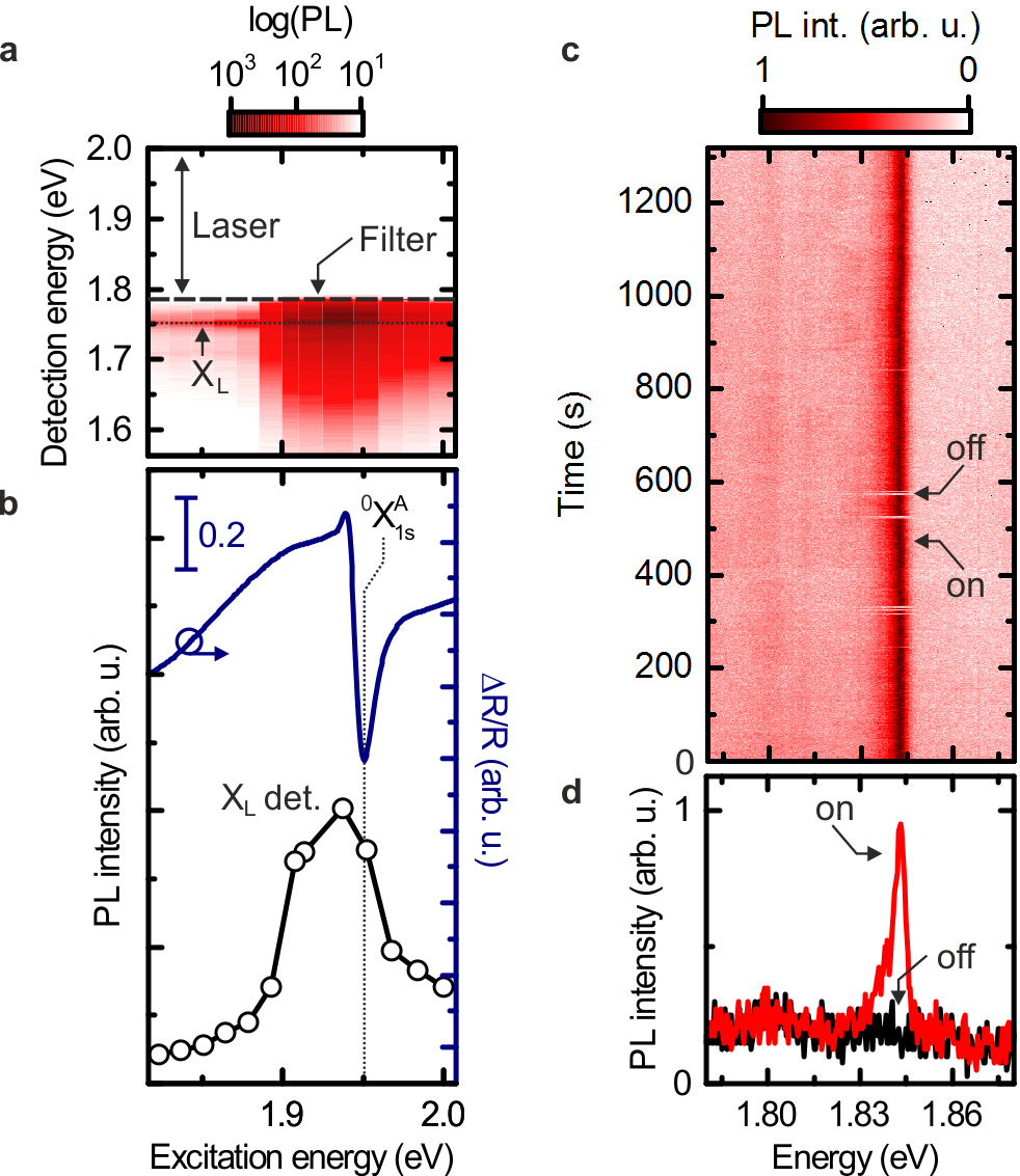
To corroborate the above interpretation of a single optically active defect, we perform photoluminescence excitation (PLE) spectroscopy to probe the photo-physics and energetic structure of the involved states. Fig. 2a presents a false color plot for a typical PLE scan of an emission line as the excitation energy is tuned across the . The emission occurs at energetically well below the . When measuring differential reflectivity using a broadband supercontinuum source, we identify at an energy of (cf. Fig. 2b). Upon resonant excitation of , the emission is significantly increased. This is a consequence of the efficient creation of excitons, when the laser energy is on resonance with an exciton transition (cf. Supplementary Information for excitation on and ). Most significantly, we can excite states also below the free exciton transitions. This is consistent with recently predicted absorbance spectra of single vacancy defects in 2D materials Refaely-Abramson et al. (2018) and in contrast to strain induced quantum dot-like emitters. Tonndorf et al. (2015); Srivastava et al. (2015); He et al. (2015); Koperski et al. (2015); Chakraborty et al. (2015); Kern et al. (2016); Branny et al. (2017); Palacios-Berraquero et al. (2017, 2017); Tonndorf et al. (2017); Blauth et al. (2018)
Another key property of quantum emitters is their spectral stability. A representative time trace of a single defect emitter is presented in Fig. 2c (with a spectrum acquired every second). Two exemplary spectra highlighted in Fig. 2c are plotted in Fig. 2d. They demonstrate that the emitter exhibits a blinking behavior. This is an observed feature of quantum emitters and more generally of various types of few-level systems. Efros and Nesbitt (2016) In our case, the blinking behavior is not surprising since the defects are embedded in a two-dimensional plane with large surface-to-volume ratio and charges in the environment that are very likely to randomly fluctuate in position and time.
Measuring the temperature dependence of the -PL spectra allows us to determine the interactions between the involved electron orbitals and phonons. We gradually change the lattice temperature from to while recording -PL spectra (cf. Fig. 3a). The spectra reveal emission from the single defect emitters that are strongly redshifted and simultaneously broadened at elevated temperatures (similar as for the ). We analyze the evolution of the emitter in detail by utilizing the independent Boson model that has been succcessfully applied to the lineshape analysis of quantum emitter states Zimmermann and Runge (2002); Wilson-Rae and Imamoğlu (2002); Krummheuer et al. (2002) and defect-bound excitons.Duke and Mahan (1965) Figure 3b highlights the spectra of for selected temperatures with lineshapes fitted by this model (red lines). In particular, the lineshape of each emitter is found to exhibit a very pronounced phonon sideband () at the low energy side. Most likely, this low energy tail results from interaction with a specific bandwidth of acoustic phonons since the defects are highly localized in real space. Refaely-Abramson et al. (2018) Our model particularly accounts for the coupling with LA/TA phonon branches, while coupling with the ZA branch is found to be negligible. For low temperatures, we find the best agreement of the calculated lineshape with our data for an effective Bohr radius of . Taking into account a phonon lifetime of , Gu et al. (2016) we obtain an excitonic radiative lifetime (linewidth) of (). The lineshape in Fig. 3b is most asymmetric at low temperatures where phonon emission is more likely to happen than phonon absorption while for higher temperatures, the lineshape becomes more symmetric.
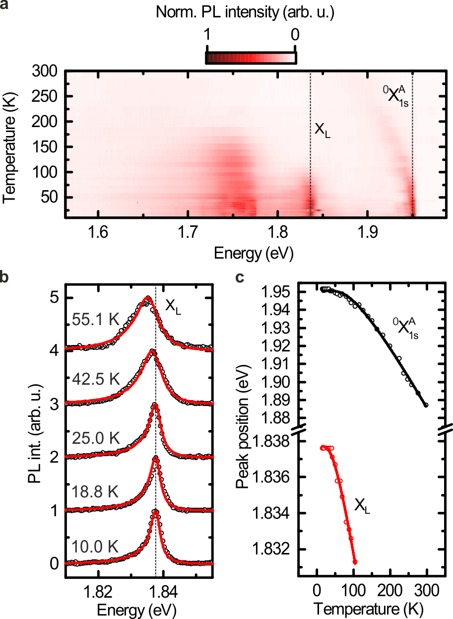
The temperature dependent peak positions in Fig. 3a manifest in the well-known polaron shift for all spectral features (compare Fig. 3c), as phenomenologically described by O’Donnell and Chen (1991)
| (2) |
with the emission energy at , the Huang-Rhys (HR) factor , the average phonon energy , and the Boltzmann constant . Fitting in Fig. 3c reveals average phonon energies of and an electron-phonon coupling (HR factor) of (for : and ). The experimental HR factor is in very good agreement with a HR factor of as obtained from the independent Boson model (cf. Supplementary Information).
III Discussion
The following arguments underline that most likely HIM induced Mo-vacancies give rise to the sharp emission lines. Importantly, the emission peaks occur homogeneously across the whole basal plane of the bombarded MoS2 encapsulated into hBN (cf. Fig. 1c). The sharp peaks do not occur in bombarded hBN without MoS2 nor in non-bombarded hBN/MoS2/hBN (cf. Supplementary Information). This phenomenology strongly suggests that the optically active defects can not be explained by single S-vacancies, because the latter are ubiquitous in exfoliated, non-bombarded MoS2 single-layers Hong et al. (2015) although they are very likely to be produced under helium ion exposure as well. Komsa et al. (2012); Noh et al. (2014); Klein et al. (2017) However, S-vacancies suffer from passivation by oxygen,Barja et al. (2018) which especially applies to the discussed nano-fabricated TMDCs under ambient conditions. Equally, quantum emitters in hBN can be excluded (cf. Supplementary Information).Tran et al. (2015) Intriguingly, the beam energy of the HIM () and also the excess energy of the secondary electrons (< ) produced in the exposed materials are sufficient to form Mo-vacancies in the MoS2, Ohya et al. (2009); Noh et al. (2014) that are rare in pristine samples.Hong et al. (2015) This argument could explain why we observe optically active defect sites only after the helium ion exposure of the MoS2 monolayers.
In our understanding, the influence of hBN is two-fold. On the one hand, the emission peaks have the lowest emission energy of of below . Encapsulated in hBN, the excitonic emission energy is renormalized due to dielectric environment, Florian et al. (2018) and particularly, the encapsulation shifts the emission energy closer to the due to a decrease of the local Coulomb interactions. On the other hand, the emission linewidth is strongly reduced for both and . Wierzbowski et al. (2017); Ajayi et al. (2017); Cadiz et al. (2017); Florian et al. (2018) The combination of the hBN-effects explain the sharp spectral features which are spread across the broad energy window in Fig. 1d. For all possibly created defects, the emission at of must resemble the lowest unoccupied, optically active state. This interpretation is consistent with the saturating behavior as in Fig. 1e, and it also explains the blinking behavior in Fig. 2c-d. Remarkably, the PLE measurements in Fig. 2a are also consistent with this interpretation, since the expected joint density of states of localized electron orbitals at the defect and its environment sum up to a finite, continuous absorbance from the lowest unoccupied state (i.e. at of ) up to . Refaely-Abramson et al. (2018) The excitation laser creates electrons that can occupy the defect states followed by optical recombination with a valence band hole and possible further local defect orbitals.Refaely-Abramson et al. (2018) In other words, the complex admixture of - and -orbitals in the Mo-defect (compare Fig. 1f-i) give rise to a continuous absorbance below , as recently discussed for single chalcogen vacancies. Noh et al. (2014); Refaely-Abramson et al. (2018) Our DFT calculation neglects the momentum dependence of the involved electron states and variable binding energies per orbital. Refaely-Abramson et al. (2018) In the experiment, the influence of ambient gases might have further effects.Klein et al. (2017)
Fig. 3b demonstrates that the effective exciton-phonon interaction can be described by the independent boson model, and the quality of the fits suggests that the effective interaction length is localized within . The independent boson model further suggests an excitonic lifetime of only 1 ps (cf. Supplementary Information). This theoretical value is a lower bound for the actual lifetime because we omit other sources of broadening mechanisms. Experimentally, we determine the upper bound of the radiative lifetime to be < (limited by the instrument response function), which renders second order time-correlation measurements of g(2) challenging. This experimental observation is in stark contrast to strain induced quantum dot-like emitters in TMDCs with nanosecond lifetimes based on an effective type-II band alignment.Tonndorf et al. (2015); Srivastava et al. (2015); He et al. (2015); Koperski et al. (2015); Chakraborty et al. (2015) Future gated devices may allow us to reduce the background PL of the so-called L-peak, so that the quantum nature of the emitted light can be further analyzed.
IV Conclusion
In conclusion, we demonstrate a methodology to deterministically generate optically active single defects in MoS2. The superior optical quality resulting from hBN encapsulation reveals spectrally narrow emission at very distinct detunings with respect to the neutral exciton. An observed saturating power dependence and a blinking behavior are consistent with the creation of single quantum emitters. On a broader perspective, a controlled production of optically active defects in a periodic pattern using helium ion beam bombardment may allow the exploration of exotic many-body physics in lattice systems, including the demonstration of coupled photon sources, Aharonovich et al. (2016) the Anderson orthogonality catastrophe, Anderson (1967); Schmidt et al. (2018) as well as the Mott transition between a superfluid and an insulator Bloch et al. (2008) in the presence of dissipation. Moreover, the inherent proximity of these engineered defect states to surfaces and their nanometer size opens exciting ways for harnessing them as quantum sensors, investigating nuclear spin physics with wave functions only sampling a fraction of atoms or studying screening physics in the ultimate limit of a single localized electronic defect state.
V Methods
V.1 Sample structure
We employed the viscoelastic transfer method to transfer MoS2 single-layer crystals and hBN multilayers onto SiO2 substrates. The MoS2 crystals used for exfoliaten were purchased from SPI Supplies while high-quality hBN bulk crystals were provided by Takashi Taniguchi and Kenji Watanabe from NIMS, Japan.
V.2 Helium Ion Microscopy
We used MoS2 monolayers transfered onto hBN/SiO2/Si substrates for He+ irradiation. A beam current and a beam energy of are used. Large areas are exposed with a beam spacing of . The dwell time was adjusted such that a dose of He+ is obtained which is optimized for a high density of single defect emitters (cf. Supplementary Information).
V.3 Optical spectroscopy
Confocal optical spectroscopy was performed in a helium flow cryostat with the sample kept at a lattice temperature of . For cw -PL experiments, we used a doubled Nd:YAG laser with an excitation energy of and typical excitation powers of less than which results in an excitation power density of at a laser spot diameter of .
For measuring differential reflectivity spectra a supercontinuum white light source was used that was focused with an optical microscope onto the sample kept at a lattice temperature of with a spot size of .
For PLE experiments, we used an optical parametric oscillator (OPO) pumped with a Ti:Sa at with a repetition rate of and a pulse width. For our measurements, we used the signal output of the OPO which was incrementally tuned in steps of from . The excitation power was kept at for all excitation energies. The excitation laser pulse was filtered with a sharp edge filter before being dispersed on a grating and detected with a charge-coupled device (CCD).
V.4 DFT calculations
The calculations were performed using density functional theory (DFT) as implemented in the Vienna ab initio simulation package (VASP) Kresse and Furthmüller (1996, 1996). The projected augmented wave method has been used Kresse and Joubert (1999); Bloechl (1994). The atomic and electronic structures were determined using the PBE functional. A plane wave basis with an energy cutoff of and a Monkhorst-Pack k-point sampling has been used. The TMD layer has been modeled using a supercell containing 242 atoms.
VI Acknowledgements
Supported by Deutsche Forschungsgemeinschaft (DFG) through the TUM International Graduate School of Science and Engineering (IGSSE). We gratefully acknowledge financial support of the German Excellence Initiative via the Nanosystems Initiative Munich and the PhD program ExQM of the Elite Network of Bavaria. We also gratefully acknowledge financial support from the European Union’s Horizon 2020 research and innovation programme under grant agreement No. 820423 (S2QUIP) the German Federal Ministry of Education and Research via the funding program Photonics Research Germany (contract number 13N14846) and the Bavarian Academy of Sciences and Humanities. M.L. and M.F. were supported by the Deutsche Forschungsgemeinschaft (DFG) within RTG 2247 and through a grant for CPU time at the HLRN (Hannover/Berlin). J.C. is supported by NSF-DMR1410599 and the Visiting Professor Program from the Bavarian State Ministry for Science, Research & the Arts. M.Kn. acknowledges support from the Technical University of Munich - Institute for Advanced Study, funded by the German Excellence Initiative and the European Union FP7 under grant agreement 291763 and the German Excellence Strategy Munich Center for Quantum Science and Technology (MCQST). R.S. acknowledges support from the Munich Center for Quantum Science and Technology (MCQST).
VII Author contributions
J.K., U.W., M.Ka., J.J.F. and A.W.H. conceived and designed the experiments, M.L. and M.F. performed the DFT and independent Boson model calculations, F.S. and J.K. prepared the samples, K.W. and T.T. provided high-quality hBN bulk crystals, J.K. performed helium ion exposure of samples, J.K., J.W., J.C. and K.M. performed the optical measurements, J.K. analyzed the data, R.S. and M.Kn. contributed interpreting the data, J.K. and A.W.H. wrote the manuscript with input from all coauthors.
VIII Additional information
VIII.1 Supplementary Information
accompanies this paper
VIII.2 Competing financial interests
The authors declare no competing financial interests.
References
- Aharonovich et al. (2016) Aharonovich, I.; Englund, D.; Toth, M. Solid-state single-photon emitters. Nature Photonics 2016, 10, 631–641.
- Ajayan et al. (2016) Ajayan, P.; Kim, P.; Banerjee, K. van der Waals materials. Physics Today 2016, 69, 9–38.
- Roldán et al. (2017) Roldán, R.; Chirolli, L.; Prada, E.; Silva-Guillén, J. A.; San-Jose, P.; Guinea, F. Theory of 2D crystals: graphene and beyond. Chem. Soc. Rev. 2017, 46, 4387–4399.
- Mak et al. (2010) Mak, K. F.; Lee, C.; Hone, J.; Shan, J.; Heinz, T. F. Atomically Thin MoS2: A New Direct-Gap Semiconductor. Physical Review Letters 2010, 105, 136805.
- Splendiani et al. (2010) Splendiani, A.; Sun, L.; Zhang, Y.; Li, T.; Kim, J.; Chim, C.-Y.; Galli, G.; Wang, F. Emerging Photoluminescence in Monolayer MoS2. Nano Letters 2010, 10, 1271–1275.
- Florian et al. (2018) Florian, M.; Hartmann, M.; Steinhoff, A.; Klein, J.; Holleitner, A. W.; Finley, J. J.; Wehling, T. O.; Kaniber, M.; Gies, C. The Dielectric Impact of Layer Distances on Exciton and Trion Binding Energies in van der Waals Heterostructures. Nano Letters 2018, 18, 2725–2732.
- Ugeda et al. (2014) Ugeda, M. M.; Bradley, A. J.; Shi, S.-F.; da Jornada, F. H.; Zhang, Y.; Qiu, D. Y.; Ruan, W.; Mo, S.-K.; Hussain, Z.; Shen, Z.-X.; Wang, F.; Louie, S. G.; Crommie, M. F. Giant bandgap renormalization and excitonic effects in a monolayer transition metal dichalcogenide semiconductor. Nature Materials 2014, 13, 1091–1095.
- Chernikov et al. (2014) Chernikov, A.; Berkelbach, T. C.; Hill, H. M.; Rigosi, A.; Li, Y.; Aslan, O. B.; Reichman, D. R.; Hybertsen, M. S.; Heinz, T. F. Exciton Binding Energy and Nonhydrogenic Rydberg Series in Monolayer WS2. Physical Review Letters 2014, 113, 076802.
- He et al. (2014) He, K.; Kumar, N.; Zhao, L.; Wang, Z.; Mak, K. F.; Zhao, H.; Shan, J. Tightly Bound Excitons in Monolayer WSe2. Physical Review Letters 2014, 113, 026803.
- Tonndorf et al. (2015) Tonndorf, P.; Schmidt, R.; Schneider, R.; Kern, J.; Buscema, M.; Steele, G. A.; Castellanos-Gomez, A.; van der Zant, H. S. J.; de Vasconcellos, S. M.; Bratschitsch, R. Single-photon emission from localized excitons in an atomically thin semiconductor. Optica 2015, 2, 347.
- Srivastava et al. (2015) Srivastava, A.; Sidler, M.; Allain, A. V.; Lembke, D. S.; Kis, A.; Imamoğlu, A. Optically active quantum dots in monolayer WSe2. Nature Nanotechnology 2015, 10, 491–496.
- He et al. (2015) He, Y.-M.; Clark, G.; Schaibley, J. R.; He, Y.; Chen, M.-C.; Wei, Y.-J.; Ding, X.; Zhang, Q.; Yao, W.; Xu, X.; Lu, C.-Y.; Pan, J.-W. Single quantum emitters in monolayer semiconductors. Nature Nanotechnology 2015, 10, 497–502.
- Koperski et al. (2015) Koperski, M.; Nogajewski, K.; Arora, A.; Cherkez, V.; Mallet, P.; Veuillen, J.-Y.; Marcus, J.; Kossacki, P.; Potemski, M. Single photon emitters in exfoliated WSe2 structures. Nature Nanotechnology 2015, 10, 503–506.
- Chakraborty et al. (2015) Chakraborty, C.; Kinnischtzke, L.; Goodfellow, K. M.; Beams, R.; Vamivakas, A. N. Voltage-controlled quantum light from an atomically thin semiconductor. Nature Nanotechnology 2015, 10, 507–511.
- Tonndorf et al. (2017) Tonndorf, P.; Schwarz, S.; Kern, J.; Niehues, I.; Pozo-Zamudio, O. D.; Dmitriev, A. I.; Bakhtinov, A. P.; Borisenko, D. N.; Kolesnikov, N. N.; Tartakovskii, A. I.; de Vasconcellos, S. M.; Bratschitsch, R. Single-photon emitters in GaSe. 2D Materials 2017, 4, 021010.
- Branny et al. (2016) Branny, A.; Wang, G.; Kumar, S.; Robert, C.; Lassagne, B.; Marie, X.; Gerardot, B. D.; Urbaszek, B. Discrete quantum dot like emitters in monolayer MoSe2: Spatial mapping, magneto-optics, and charge tuning. Applied Physics Letters 2016, 108, 142101.
- Palacios-Berraquero et al. (2017) Palacios-Berraquero, C.; Kara, D. M.; Montblanch, A. R.-P.; Barbone, M.; Latawiec, P.; Yoon, D.; Ott, A. K.; Loncar, M.; Ferrari, A. C.; Atatüre, M. Large-scale quantum-emitter arrays in atomically thin semiconductors. Nature Communications 2017, 8, 15093.
- Kern et al. (2016) Kern, J.; Niehues, I.; Tonndorf, P.; Schmidt, R.; Wigger, D.; Schneider, R.; Stiehm, T.; de Vasconcellos, S. M.; Reiter, D. E.; Kuhn, T.; Bratschitsch, R. Nanoscale Positioning of Single-Photon Emitters in Atomically Thin WSe2. Advanced Materials 2016, 28, 7101–7105.
- Branny et al. (2017) Branny, A.; Kumar, S.; Proux, R.; Gerardot, B. D. Deterministic strain-induced arrays of quantum emitters in a two-dimensional semiconductor. Nature Communications 2017, 8, 15053.
- Blauth et al. (2018) Blauth, M.; Jürgensen, M.; Vest, G.; Hartwig, O.; Prechtl, M.; Cerne, J.; Finley, J. J.; Kaniber, M. Coupling Single Photons from Discrete Quantum Emitters in WSe2 to Lithographically Defined Plasmonic Slot Waveguides. Nano Letters 2018,
- Laucht et al. (2012) Laucht, A.; Pütz, S.; Günthner, T.; Hauke, N.; Saive, R.; Frédérick, S.; Bichler, M.; Amann, M.-C.; Holleitner, A. W.; Kaniber, M.; Finley, J. J. A Waveguide-Coupled On-Chip Single-Photon Source. Physical Review X 2012, 2.
- Reithmaier et al. (2015) Reithmaier, G.; Kaniber, M.; Flassig, F.; Lichtmannecker, S.; Müller, K.; Andrejew, A.; Vučković, J.; Gross, R.; Finley, J. J. On-Chip Generation, Routing, and Detection of Resonance Fluorescence. Nano Letters 2015, 15, 5208–5213.
- Goodfellow et al. (2014) Goodfellow, K. M.; Beams, R.; Chakraborty, C.; Novotny, L.; Vamivakas, A. N. Integrated nanophotonics based on nanowire plasmons and atomically thin material. Optica 2014, 1, 149.
- Goodfellow et al. (2015) Goodfellow, K. M.; Chakraborty, C.; Beams, R.; Novotny, L.; Vamivakas, A. N. Direct On-Chip Optical Plasmon Detection with an Atomically Thin Semiconductor. Nano Letters 2015, 15, 5477–5481.
- Blauth et al. (2017) Blauth, M.; Harms, J.; Prechtl, M.; Finley, J. J.; Kaniber, M. Enhanced optical activity of atomically thin MoSe2 proximal to nanoscale plasmonic slot-waveguides. 2D Materials 2017, 4, 021011.
- Fox et al. (2015) Fox, D. S. et al. Nanopatterning and Electrical Tuning of MoS2 Layers with a Subnanometer Helium Ion Beam. Nano letters 2015, 15, 5307–5313.
- Tongay et al. (2013) Tongay, S.; Suh, J.; Ataca, C.; Fan, W.; Luce, A.; Kang, J. S.; Liu, J.; Ko, C.; Raghunathanan, R.; Zhou, J.; Ogletree, F.; Li, J.; Grossman, J. C.; Wu, J. Defects activated photoluminescence in two-dimensional semiconductors: interplay between bound, charged, and free excitons. Scientific reports 2013, 3, 2657.
- Klein et al. (2017) Klein, J.; Kuc, A.; Nolinder, A.; Altzschner, M.; Wierzbowski, J.; Sigger, F.; Kreupl, F.; Finley, J. J.; Wurstbauer, U.; Holleitner, A. W.; Kaniber, M. Robust valley polarization of helium ion modified atomically thin MoS2. 2D Materials 2017, 5, 011007.
- Aharonovich et al. (2016) Aharonovich, I.; Englund, D.; Toth, M. Solid-state single-photon emitters. Nature Photonics 2016, 10, 631–641.
- Anderson (1967) Anderson, P. W. Infrared Catastrophe in Fermi Gases with Local Scattering Potentials. Physical Review Letters 1967, 18, 1049–1051.
- Schmidt et al. (2018) Schmidt, R.; Knap, M.; Ivanov, D. A.; You, J.-S.; Cetina, M.; Demler, E. Universal many-body response of heavy impurities coupled to a Fermi sea. Rep. Prog. Phys. 2018, 81, 024401.
- Bloch et al. (2008) Bloch, I.; Dalibard, J.; Zwerger, W. Many-body physics with ultracold gases. 2008, 80, 885–80.
- Wierzbowski et al. (2017) Wierzbowski, J.; Klein, J.; Sigger, F.; Straubinger, C.; Kremser, M.; Taniguchi, T.; Watanabe, K.; Wurstbauer, U.; Holleitner, A. W.; Kaniber, M.; Müller, K.; Finley, J. J. Direct exciton emission from atomically thin transition metal dichalcogenide heterostructures near the lifetime limit. Scientific Reports 2017, 7.
- Ajayi et al. (2017) Ajayi, O. A.; Ardelean, J. V.; Shepard, G. D.; Wang, J.; Antony, A.; Taniguchi, T.; Watanabe, K.; Heinz, T. F.; Strauf, S.; Zhu, X.-Y.; Hone, J. C. Approaching the intrinsic photoluminescence linewidth in transition metal dichalcogenide monolayers. 2D Materials 2017, 4, 031011.
- Cadiz et al. (2017) Cadiz, F. et al. Excitonic Linewidth Approaching the Homogeneous Limit in MoS2 -Based van der Waals Heterostructures. Physical Review X 2017, 7.
- Korn et al. (2011) Korn, T.; Heydrich, S.; Hirmer, M.; Schmutzler, J.; Schüller, C. Low-temperature photocarrier dynamics in monolayer MoS2. Applied Physics Letters 2011, 99, 102109.
- Carozo et al. (2017) Carozo, V.; Wang, Y.; Fujisawa, K.; Carvalho, B. R.; McCreary, A.; Feng, S.; Lin, Z.; Zhou, C.; Perea-López, N.; Elías, A. L.; Kabius, B.; Crespi, V. H.; Terrones, M. Optical identification of sulfur vacancies: Bound excitons at the edges of monolayer tungsten disulfide. Science Advances 2017, 3, e1602813.
- Noh et al. (2014) Noh, J.-Y.; Kim, H.; Kim, Y.-S. Stability and electronic structures of native defects in single-layer . Phys. Rev. B 2014, 89, 205417.
- Refaely-Abramson et al. (2018) Refaely-Abramson, S.; Qiu, D. Y.; Louie, S. G.; Neaton, J. B. Defect-Induced Modification of Low-Lying Excitons and Valley Selectivity in Monolayer Transition Metal Dichalcogenides. Phys. Rev. Lett. 2018, 121, 167402.
- Efros and Nesbitt (2016) Efros, A. L.; Nesbitt, D. J. Origin and control of blinking in quantum dots. Nature Nanotechnology 2016, 11, 661–671.
- Zimmermann and Runge (2002) Zimmermann, R.; Runge, E. Dephasing in quantum dots via electron-phonon interaction. Proc. 26th ICPS, Edinburgh 2002,
- Wilson-Rae and Imamoğlu (2002) Wilson-Rae, I.; Imamoğlu, A. Quantum dot cavity-QED in the presence of strong electron-phonon interactions. Phys. Rev. B 2002, 65, 235311.
- Krummheuer et al. (2002) Krummheuer, B.; Axt, V. M.; Kuhn, T. Theory of pure dephasing and the resulting absorption line shape in semiconductor quantum dots. Physical Review B 2002, 65.
- Duke and Mahan (1965) Duke, C. B.; Mahan, G. D. Phonon-Broadened Impurity Spectra. I. Density of States. Phys. Rev. 1965, 139, A1965–A1982.
- Gu et al. (2016) Gu, X.; Li, B.; Yang, R. Layer thickness-dependent phonon properties and thermal conductivity of MoS2. Journal of Applied Physics 2016, 119, 085106.
- O’Donnell and Chen (1991) O’Donnell, K. P.; Chen, X. Temperature dependence of semiconductor band gaps. Applied Physics Letters 1991, 58, 2924–2926.
- Hong et al. (2015) Hong, J. et al. Exploring atomic defects in molybdenum disulphide monolayers. Nature communications 2015, 6, 6293.
- Komsa et al. (2012) Komsa, H.-P.; Kotakoski, J.; Kurasch, S.; Lehtinen, O.; Kaiser, U.; Krasheninnikov, A. V. Two-dimensional transition metal dichalcogenides under electron irradiation: defect production and doping. Physical review letters 2012, 109, 035503.
- Barja et al. (2018) Barja, S. et al. Identifying substitutional oxygen as a prolific point defect in monolayer transition metal dichalcogenides with experiment and theory. arXiv preprint arXiv:1810.03364 2018,
- Tran et al. (2015) Tran, T. T.; Bray, K.; Ford, M. J.; Toth, M.; Aharonovich, I. Quantum emission from hexagonal boron nitride monolayers. Nature Nanotechnology 2015, 11, 37–41.
- Ohya et al. (2009) Ohya, K.; Yamanaka, T.; Inai, K.; Ishitani, T. Comparison of secondary electron emission in helium ion microscope with gallium ion and electron microscopes. Nuclear Instruments and Methods in Physics Research Section B: Beam Interactions with Materials and Atoms 2009, 267, 584–589.
- Kresse and Furthmüller (1996) Kresse, G.; Furthmüller, J. Efficiency of Ab-initio Total Energy Calculations for Metals and Semiconductors using a Plane-wave Basis Set. Comput. Mat. Sci. 1996, 6, 15–50.
- Kresse and Furthmüller (1996) Kresse, G.; Furthmüller, J. Efficient Iterative Schemes for Ab-initio Total-energy Calculations using a Plane-wave Basis Set. Phys. Rev. B 1996, 54, 11169–11186.
- Kresse and Joubert (1999) Kresse, G.; Joubert, D. From Ultrasoft Pseudopotentials to the Projector Augmented-wave Method. Phys. Rev. B 1999, 59, 1758–1775.
- Bloechl (1994) Bloechl, P. Projector Augmented-wave Method. Phys. Rev. B 1994, 50, 17953–17979.