SFQmap: A Technology Mapping Tool for Single Flux Quantum Logic Circuits
Abstract
Single flux quantum (SFQ) logic is a promising candidate to replace the CMOS logic for high speed and low power applications due to its superiority in providing high performance and energy efficient circuits. However, developing effective Electronic Design Automation (EDA) tools, which cater to special characteristics and requirements of SFQ circuits such as depth minimization and path balancing, are essential to automate the whole process of designing large SFQ circuits. In this paper, a novel technology mapping tool, called SFQmap, is presented, which provides optimization methods for minimizing first the circuit depth and path balancing overhead and then the worst-case stage delay of mapped SFQ circuits. Compared with the state-of-the-art technology mappers, SFQmap reduces the depth and path balancing overhead by an average of 14% and 31%, respectively.
I Introduction
Logic synthesis is an important step in the design flow of digital circuits and systems with a big impact on the final delay and area of the chip. Logic synthesis has two main phases: technology-independent optimizations, and technology mapping. The first phase includes several algebraic or Boolean optimizations such as restructuring, resubstitution, common subexpression extraction, node minimization. The second phase performs mapping or binding of logic expressions to actual gates in a given cell library to minimize the circuit delay, area or other desired metrics.
Rapid SFQ (RSFQ) is a family of Single Flux Quantum circuits, which was developed in late 1980s [1]. More recent versions of SFQ logic family include ERSFQ [2, 3] and eSFQ [4] as well as AQFP [5]. Generally, SFQ logic has been touted as a good candidate for achieving energy efficient and high performance circuits [6]. SFQ devices are made of Josephson Junctions, which are superconducting devices that exhibit the Josephson effect, i.e., the phenomenon of a current (called super-current) that flows indefinitely long without any applied voltage. The propagation delay through these devices is as low as , while each switching action consumes in the order of energy [7]. The JJ switching energy is 2-3 orders of magnitude lower than that of the end-of-CMOS-scaling devices as stated in [8], which again shows the promise of SFQ circuits as a replacement for CMOS circuits. SFQ gates can operate as fast as 370GHz at [7].
Although advantages of SFQ logic in achieving super fast and very low-power circuits have been proven, state of the art in Electronic Design Automation (EDA) technologies is not advanced. On the other hand, due to key differences between SFQ and CMOS logic, CMOS Computer Aided Design (CAD) tools cannot be directly used to optimize SFQ circuits. Therefore, it is critical to develop appropriate CAD tools including synthesis, place and route, timing and power analysis, and verification tools to fully automate the design and test process of SFQ circuits.
In this paper, we present SFQmap, a technology mapping tool for SFQ circuits. To the best of authors’ knowledge, this is the first paper which presents a technology mapping tool designed specifically for optimizing SFQ circuits. There are some tools for logic synthesis of SFQ, but they either provide simple optimizations or are based on standard CMOS CAD tools with minor pre or post optimizations (Section III-A). SFQmap includes two main phases: (i) logical depth minimization with path balancing, and (ii) peephole optimization to reduce the worst-case delay of any stage of the logic circuit. SFQmap improves key parameters of SFQ circuits considerably compared with the state-of-the-art technology mappers. For example, it decreases the number of path balancing D-Flip-Flops (DFFs), and the Product of the worst-case Stage delay with the logical Depth of the circuit (which we shall denote as PSD) by up to 43%, and 63%, respectively (Section IV).
II Background
II-A Background on SFQ (SFQ Basics)
Single Flux Quantum (SFQ) logic uses a single quantum of magnetic flux () to represent the binary information. This SFQ typically appears as a voltage pulse with a peak amplitude of 2-4mV and a duration of 1-2ps. In this representation, the presence of a SFQ pulse is considered as “logic-1”, while the absence of the pulse is interpreted as “logic-0” [9]. In the following, we explain characteristics and key circuit/gate level requirements of SFQ logic.
II-A1 Fanout in SFQ
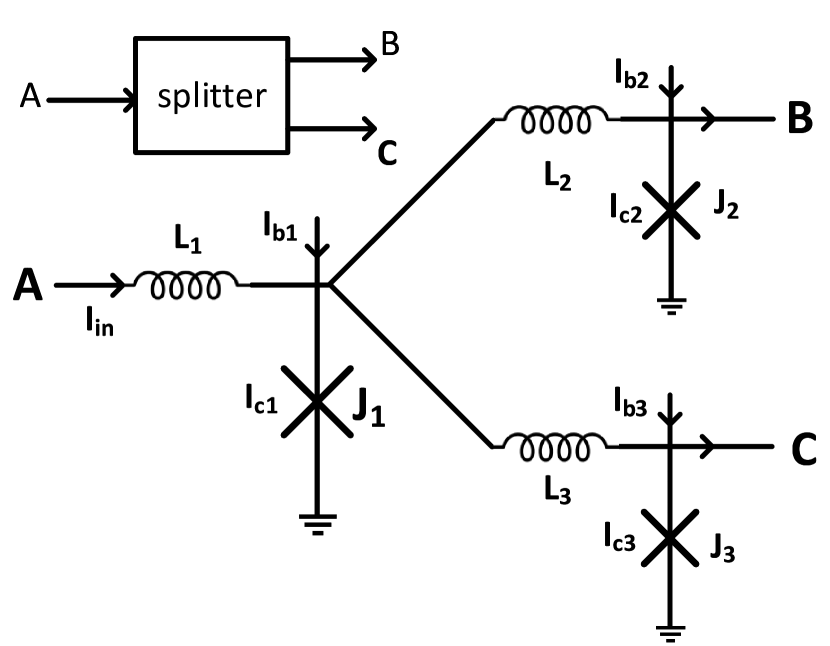
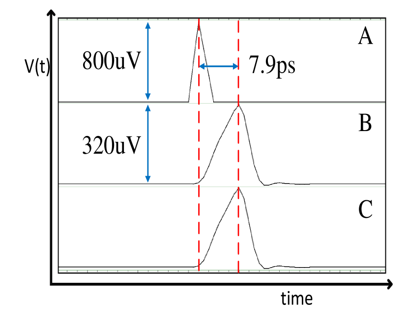
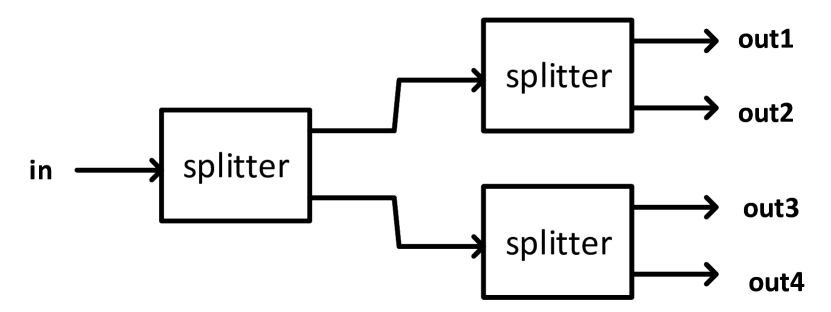
In conventional SFQ logic, each gate can only drive one other node (fanout count is one). If a gate needs to have more than one fanout, an special SFQ gate called a splitter cell is inserted at the output of that gate to enable fanout to two gates. To support additional fanouts, a binary tree of splitter cells can be used. Fig. 1 shows the circuit-level schematic of a splitter gate, its corresponding waveform, and an example of a splitter tree for fanout of 4 (FO4).
II-A2 Gate-level pipeline
All SFQ gates, except splitters, require a clock signal to transfer the stored quantum flux to their output. In addition, operation of all SFQ gates is synchronized by the clock. For distribution of the clock signal in a SFQ chip, there are three main methods: counter-flow clocking in which the clock flows in the opposite direction of the data, concurrent-flow clocking, where clock and data flow in the same direction, and clock-follow-data, in which the clock arrives after the data input to a gate have arrived and been processed by the gate. For more information on the clock distribution network of the SFQ circuits, please refer to [11, 10]. The take-away is that nearly all SFQ gates (with the exception of some asynchronous gates such as a splitter or a Josephson Transmission Line) can be thought of as purely combinational gates followed by clocked DFFs. The combinational gate responds to its inputs by changing its internal loop current state whereas the gate output will change only after the clock pulse comes, which will in turn reset the gate’s internal state while producing the correct gate output value. In other words, every SFQ circuit must be completely gate-level pipelined.
II-A3 Path Balancing
Due to gate-level pipelining in SFQ, for correct operation of the SFQ gates, all inputs of a gate should have the same logic level111Logic level of gate denotes the length of the longest path (in terms of the gate count) from any Primary Input (PI) of the network to this gate.. If inputs of a gate do not have the same logic level, some DFFs should be inserted into the path with smaller depth to balance the network. For example, if the first input () in an AND2 gate has the logic level of 2 and the second input () has the logic level of 3, one DFF should be added to . This path balancing is needed because once the clock arrives at a gate, the available input data (which is stored as a loop current in the gate) is reset in order to produce the correct output value. So, if inputs to a gate arrive too early or too late, the gate will produce wrong results when corresponding clock pulses arrive at the gate. In the above example, if and are both logic 1 values, arrives early, but does not arrive until after the clock pulse has come in (the AND2 gate will produce a wrong output result of logic 0 in response to the clock pulse.)
II-A4 Product of Stage Delay and Circuit Depth
Due to the gate-level pipelined nature of the SFQ logic, the input-to-output latency of a SFQ circuit is determined as the product of the clock cycle time and the logical depth of the circuit. The clock cycle time is in turn set by the worst-case delay of any single stage (gate plus any present splitters plus interconnect) of logic in the circuit.
III Technology Mapping
III-A Prior Work
In [12, 13], a tree mapping and decomposition method is presented to generate minimum area or low power circuits. In [14], a cut-enumeration-based method which involves cut generation and cut selection was presented targeting the depth-optimal area optimization for the FPGAs. For the SFQ circuits, there are couple of papers addressing the logic synthesis [15, 16, 17]. In [15], a framework is proposed for synthesizing the SFQ circuits by constructing a virtual cell called “2-AND/XOR”. In [16], a top-down design methodology for the SFQ circuits based on the Binary Decision Diagram (BDD) is presented. In [17], an academic logic synthesis tool (ABC)[18] is modified to meet the requirements of SFQ logic without developing any SFQ specific optimization algorithms for the technology mapping.
III-B Motivation
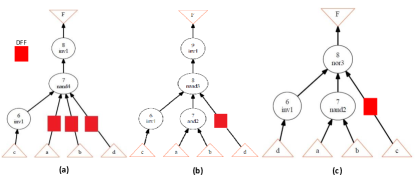
To map the Boolean expression, , the ABC mapper [18] produces the circuit shown in Fig. 2(a). As explained in Section II-A3, the SFQ circuits need to be path balanced. Thus, for the mapped circuit generated by ABC, three path balancing DFFs have to be inserted into the network. Another circuit with fewer number of required path balancing DFFs can be found to implement the given Boolean expression, as shown in Fig. 2(b). On the other hand, as discussed in Section II-A4, to reduce the computation latency, the PSD should be minimized. In practice, between the logical depth and the worst-case stage delay, the former has more impact on the overall computation latency; therefore, we target the minimization of the logical depth (along with minimization of the path-balancing DFF overhead) first; Only after this optimization is done we turn to direct minimization of the product of the stage delay and logical depth. Based on this explanation, the circuit shown in Fig. 2(c) is more desirable than the other two . This is because it requires only one DFF while its logical depth is less. We need to develop a technology mapper for SFQ which prefers the circuit shown in Fig. 2(c) over the other two mapping solutions.
III-C Algorithms
Our proposed technology mapping for the SFQ circuits consists of two main phases: depth minimization and path balancing, and peephole optimization for reducing the PSD. The aforesaid phases are discussed in more details in the following.
III-C1 Depth Minimization with Path Balancing
In this sub-section, we present the problem of tree-mapping as a Dynamic Programming (DP) problem. The optimal solution is the one with the least depth and in the case of a tie, it is the one which requires less number of path balancing DFFs. A similar cut-enumeration methods as in [19, 20] is used. As mentioned in [19], this method provides the optimal depth solution for general DAGs. The main difference between the method which is presented in [19] and our depth minimization and path balancing method is that we optimize both depth and balancing, while in [19] only depth is considered.
Fig. 3 shows a binary tree and the - cuts for node . (refer to [19] for the definition of - cuts.) Eq. III-C1 defines the value of optimal depth solution, , as the minimum achievable logical depth for mapping a tree rooted at node . is calculated recursively as follows:
| (1) |
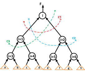
The three terms in the Eq. III-C1 corresponds to the depth of cuts (Fig. 3), respectively. Basically, in Eq. III-C1 a mapping solution with the least depth () among all choices corresponding to the - cuts is being computed. Among all the solutions with depth , the one which requires fewer path balancing DFFs is selected recursively in a Dynamic Programming approach as shown in Eq. 2. In this equation, gives the DFF count for a solution with depth of and the least number of path balancing DFFs (#DFFs).
| (2) |
In the above equation, accounts for the required number of DFFs for balancing the inputs of the corresponding cut because of the level difference among cut’s inputs. For example, if the level of node + is and + is , ++ returns .
The complexity of computing the - cuts is , where is the edge count, and is the node count [19]. The complexity of our depth minimization and path balancing algorithm by having the - cuts is , where is the maximum number of - cuts for a node in the network, is the number of gates in the library, and is the total number of nodes in the network. Usually and are small numbers. Thus, the complexity for this algorithm is determined by the number of nodes in the network with linear relationship ().
| #DFFs | #Gates | Logical Depth | PSD | Run-time | ||||||
|---|---|---|---|---|---|---|---|---|---|---|
| Circuits | SFQmap | ABC | SFQmap | ABC | SFQmap | ABC | SFQmap | ABC | SFQmap | ABC |
| s4863 | 3381 | 4274 | 1183 | 1010 | 30 | 36 | 297 | 378 | 0.198 | 0.15 |
| c5315 | 2519 | 4437 | 1399 | 1206 | 20 | 25 | 179 | 234 | 0.2 | 0.12 |
| c7552 | 2603 | 3639 | 1786 | 1457 | 19 | 21 | 267.9 | 718.2 | 0.25 | 0.22 |
| s6669 | 7621 | 9638 | 1517 | 1462 | 46 | 52 | 510.6 | 842.4 | 0.258 | 0.145 |
| s38417 | 13953 | 23253 | 8363 | 7471 | 14 | 16 | 180.6 | 252.8 | 0.667 | 0.32 |
| Mapper | Logical Depth | #DFFs | PSD | Run-time |
|---|---|---|---|---|
| SFQmap -i 5 | 14% | 31% | 35% | 34% |
| SFQmap -i 0 | 15% | 37% | 13% | 12% |
III-C2 Peephole Optimization for Reducing the Sequential Depth
As explained in Section II-A4, despite in CMOS, in the SFQ circuits to reduce the computation latency, PSD has to be reduced. To reduce the PSD, we perform the following heuristic:
After finding the minimum depth and most balanced solution for each node of the network as in Section III-C1, a gate with the worst stage delay is found. This gate is usually a gate with high fanout count. Next, a temporary network consisting this gate and its immediate fanins and fanouts is generated. The temporary network is re-mapped while the fanout count for any node is limited. If the product of the worst stage delay and the length of the longest path decreased, the move will be accepted. Otherwise, we increase the fanout counts’ limit and re-do the process. This process is repeated times. Experimental results show that for having , there will be a considerable decrease in the PSD of the circuit while the run-time is acceptable (Tables I,II).
The complexity of the peephole optimization is , where, is the edge count and is the node count of the network. This is because for calculating the fanout dependent stage delay for all nodes (to find the worst stage delay), a breath-first search should be done. The peephole optimization determines the overall complexity of the SFQmap tool to be .
Algorithm 1 describes the pseudo code of the SFQmap. In this algorithm, the main procedure as well as functions for combined depth minimization and path balancing, and then peephole optimization for reducing the PSD are shown.
IV Experimental Results
We implemented our SFQ specific technology mapping algorithms inside ABC [18]. We used several ISCAS benchmark circuits [21] for testing our developed technology mapper. The mcnc.genlib library is used. Table I lists the key parameters for different benchmark circuits for SFQmap and ABC technology mapping tools. As explained in Section III-C, our developed technology mapper focuses on improving three important parameters in SFQ circuits including logical depth, #DFFs, and PSD. As shown in Tables I,II, SFQmap provides considerable improvements on all of these critical parameters on average of all five benchmark circuits. However, its average run-time is increased by 34% over the ABC mapper. This is mainly because of the peephole optimization phase which dominates the run-time of the SFQmap. We implemented the peephole optimization phase with the capability of determining the number of iterations. The experimental results in the Table I is for five iterations of peephole optimization (SFQmap -i 5). If we cross out the peephole optimization phase to trade the PSD with the run-time, the run-time overhead over the ABC mapper will be decreased to less than 12%. In Table II, “SFQmap -i 0” is for not having any peephole optimization runs. stands for the number of iterations.
V Conclusion
In this paper, a novel technology mapping tool, SFQmap, is presented which is developed for the SFQ circuits. This mapper performs two main optimizations to improve the most important parameters for the SFQ circuits including the logical depth, the number of path balancing DFFs, and the PSD. The implementation of this mapper allows to select the number of iterations for the optimization runs. “SFQmap -i 5” improves the logical depth, #DFFs, and the PSD by 14%, 31%, and 35%, respectively over the ABC [18] mapper for five ISCAS benchmark circuits with 34% increase in run-time. “SFQmap -i 0” reduces the overhead of run-time to less than 12% and provides even more improvements on the logical depth, and #DFFs over ABC (see Table II).
VI Acknowledgement
The research is based upon work supported by the Office of the Director of National Intelligence (ODNI), Intelligence Advanced Research Projects Activity (IARPA), via the U.S. Army Research Office grant W911NF-17-1-0120. The U.S. Government is authorized to reproduce and distribute reprints for Governmental purposes notwithstanding any copyright notation herein.
References
- [1] K. Likharev and V. Semenov, “Rsfq logic/memory family: A new josephson-junction technology for sub-terahertz-clock-frequency digital systems,” IEEE Transactions on Applied Superconductivity, vol. 50, no. 1, 1991.
- [2] A. F. Kirichenko, S. Sarwana, and I. V. Vernik, “Ersfq-zero static power dissipation single flux quantum logic,” in Government Microcircuit Appl. and Critical Techn. Conf.(GOMACTech-12), pp. 319–322.
- [3] O. Mukhanov, V. Semenov, and K. Likharev, “Ultimate performance of the rsfq logic circuits,” IEEE Transactions on Magnetics, vol. 23, no. 2, pp. 759–762, 1987.
- [4] O. A. Mukhanov, “Energy-efficient single flux quantum technology,” IEEE Transactions on Applied Superconductivity, vol. 21, no. 3, pp. 760–769, 2011.
- [5] N. Takeuchi, Y. Yamanashi, and N. Yoshikawa, “Energy efficiency of adiabatic superconductor logic,” Superconductor Science and Technology, vol. 28, no. 1, p. 015003, 2014.
- [6] D. S. Holmes, A. L. Ripple, and M. A. Manheimer, “Energy-efficient superconducting computing-power budgets and requirements,” IEEE Transactions on Applied Superconductivity, vol. 23, no. 3, pp. 1 701 610–1 701 610, 2013.
- [7] P. Bunyk, A. Oliva, V. Semenov, M. Bhushan, K. Likharev, J. Lukens, M. Ketchen, and W. Mallison, “High-speed single-flux-quantum circuit using planarized niobium-trilayer josephson junction technology,” Applied physics letters, vol. 66, no. 5, pp. 646–648, 1995.
- [8] T. N. Theis and H. S. P. Wong, “The end of moore’s law: A new beginning for information technology,” Computing in Science Engineering, vol. 19, no. 2, pp. 41–50, Mar 2017.
- [9] R. Gross, A. Marx, and F. Deppe, Applied superconductivity: Josephson effect and superconducting electronics. De Gruyter, 2015.
- [10] N. Katam, A. Shafaei, and M. Pedram, “Design of multiple fanout clock distribution network for rapid single flux quantum technology,” in Design Automation Conference (ASP-DAC), 2017 22nd Asia and South Pacific. IEEE, 2017, pp. 384–389.
- [11] E. G. Friedman, “Clock distribution networks in synchronous digital integrated circuits,” Proceedings of the IEEE, vol. 89, no. 5, pp. 665–692, 2001.
- [12] K. Keutzer, “Dagon: technology binding and local optimization by dag matching,” in Design Automation, 1987. 24th Conference on. IEEE, 1987, pp. 341–347.
- [13] K. Chaudhary and M. Pedram, “Computing the area versus delay trade-off curves in technology mapping,” IEEE Transactions on Computer-Aided Design of Integrated Circuits and Systems, vol. 14, no. 12, pp. 1480–1489, 1995.
- [14] D. Chen and J. Cong, “Daomap: A depth-optimal area optimization mapping algorithm for fpga designs,” in Proceedings of the 2004 IEEE/ACM International conference on Computer-aided design. IEEE Computer Society, 2004, pp. 752–759.
- [15] S. Yamashita, K. Tanaka, H. Takada, K. Obata, and K. Takagi, “A transduction-based framework to synthesize rsfq circuits,” in Proceedings of the 2006 Asia and South Pacific Design Automation Conference (ASP-DAC). IEEE Press, 2006, pp. 266–272.
- [16] N. Yoshikawa and J. Koshiyama, “Top-down rsfq logic design based on a binary decision diagram,” IEEE transactions on applied superconductivity, vol. 11, no. 1, pp. 1098–1101, 2001.
- [17] N. Katam, A. Shafaei, and M. Pedram, “Design of complex rapid single-flux-quantum cells with application to logic synthesis,” in 16th International Superconductive Electronics Conference, ISEC 2017.
- [18] U. Berkeley, “ABC: A system for sequential synthesis and verification,” Berkeley Logic Synthesis and Verification Group, 2011.
- [19] J. Cong and Y. Ding, “Flowmap: An optimal technology mapping algorithm for delay optimization in lookup-table based fpga designs,” IEEE Transactions on Computer-Aided Design of Integrated Circuits and Systems, vol. 13, no. 1, pp. 1–12, 1994.
- [20] A. Mishchenko, S. Cho, S. Chatterjee, and R. Brayton, “Combinational and sequential mapping with priority cuts,” in Proceedings of the 2007 IEEE/ACM international conference on Computer-aided design. IEEE Press, 2007, pp. 354–361.
- [21] M. C. Hansen, H. Yalcin, and J. P. Hayes, “Unveiling the iscas-85 benchmarks: A case study in reverse engineering,” IEEE Design & Test of Computers, vol. 16, no. 3, pp. 72–80, 1999.