First principles study of ferroelastic twins in halide perovskites
Abstract
We present an ab initio simulation of ferroelastic twins that were recently observed in methyl ammonium lead iodide Rothmann et al. (2017). There are two inequivalent types of walls that we calculate to act as either electron or hole sinks which suggests a possible route to enhancing charge carrier separation in photovoltaic devices. Despite separating non-polar domains, we show these walls to have a substantial in-plane polarisation of , due in part to flexoelectricity. We suggest this in turn could allow for the photoferroic effect and create efficient pathways for photocurrents within the wall.
I Introduction
The synthesis of a hybrid organic-inorganic halide pervoskite (‘HOIP’) solar cell was first reported in 2009 Kojima et al. (2009). Since then, the power conversion efficiencies (PCE) of these devices have climbed rapidly from 14.3% to 23.7% NRE . A wide range of materials, in particular methylammonium lead iodide (, ‘MAPI’), have been considered to investigate this class of photovoltaic devices. Key issues regarding the stability and efficiency of these materials are an ongoing area of research (cf. reviews Bhatt and Lee (2017); Huang et al. (2017) and references therein), not least of which is the origin of their high PCE. In this context, one important issue still undergoing investigation is whether MAPI is ferroelectric and, by extension, how the photoferroic effect Fridkin (1979); Sturman and Fridkin (1992); Butler et al. (2015) might play a role in the reported PCEs. As of yet, there is no clear consensus on the former issue Frost et al. (2014); Kutes et al. (2014); Fan et al. (2015); G et al. (2016); Kim et al. (2016); Rakita et al. (2017); Hoque et al. (2016). In addition to multiple related studies on the bulk material, there have been a number of publications on planar defects such as grain boundaries and domain walls which we briefly summarise here (more detailed reviews can be found in Whalley et al. (2017); Liu et al. (2018a)).
At a defect boundary, properties not present in the bulk may emerge at the interface itself, chiefly due to the local structural distortion. For instance, a bulk property may change orientation across the boundary and thus some components will locally vanish or be enhanced. Hence, physics that is ordinarily suppressed in the bulk may manifest at the wall. Theoretical studies on grain boundaries Shan and Saidi (2017); Yin et al. (2014); McKenna (2018); Guo et al. (2017); Yin et al. (2015) and ferroelectric domain walls Liu et al. (2015); Chen et al. ; Frost et al. (2014) have proposed a variety of ways in which these types of planar defects may influence the electronic properties of HOIPs. Some first–principles simulations suggest that the presence of grain boundaries is not detrimental to photovoltaic performance Guo et al. (2017); Yin et al. (2015, 2014). Conversely, experimental evidence indicates charge carrier recombination is enhanced at these defects Bischak et al. (2015). It has been proposed that ferroelectric domain walls (‘twins’) can be formed via interfacing polar domains in which the methyl ammonium (MA) molecular dipoles are aligned. Calculations on these twins indicate beneficial effects such as locally diminished band gaps Liu et al. (2015); Chen et al. or enhanced charge carrier diffusion lengths Frost et al. (2014).
Recently, ferroelastic twins in MAPI were observed at room temperature and their structure has been determined Rothmann et al. (2017); Liu et al. (2018b, c). We emphasise that these types of defect are distinct from the aforementioned grain boundaries and ferroelectric twins. Ferroelastic domain walls separate domains with different strain states. Unlike a general grain boundary, the domains are ‘crystallographically’ related ITD and, in contrast to ferroelectric twins, these domains can be non-polar (which may be the case in MAPI). Nonetheless, to the best of our knowledge, an ab initio simulation of the ferroelastic twins observed and described here has not been carried out.
Here, we report a density-functional theory simulation of the twins characterised in Rothmann et al. (2017); Liu et al. (2018b, c). We find the walls to be thin, polar and have a low formation energy. The effect of these properties on the photovoltaic performance of halide perovkistes is discussed in addition to possible avenues for domain-wall engineering such devices.
II Methods & computational details
There are obvious technical challenges to account for the dynamic ordering of MA molecules in a zero Kelvin calculation. Hence we studied these walls in , the Cs atom having a similar effective size to the MA molecule Lee et al. (2016). Furthemore, the valence and conduction band edges are known to be mainly dominated by Pb and I states Brivio et al. (2013). Hence, we expect MAPI twins to display the properties presented here with additional physics arising from the organic molecule. In addition, the use of in synthesising photovoltaic devices Eperon et al. (2015) and doping MAPI with Cs to improve PCE Choi et al. (2014) make this topical in its own right.
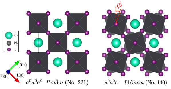
MAPI and adopt the perovskite structure of corner-sharing octahedra with MA+/Cs+ and Pb2+ cubic sub–lattices. We studied the room temperature tetragonal phase of MAPI with where the octahedra tilt in antiphase with angle along one tetrad axis (shown in Fig. 1). The phase has space group (No. 140) Weller et al. (2015) with Glazer tilt pattern (indicating no octahedral tilts about [100] and [010] directions and an antiphase tilt about the [001] axis Glazer (1972)). This single domain state may be characterised by a pseudovector parallel to the tilt axis and whose magnitude is equal to the tilt angle . Note that the symmetry of this anti-phase tilt makes the space group necessarily non-polar. Due to the spontaneous strain induced by , such a state is termed improper ferroelastic.
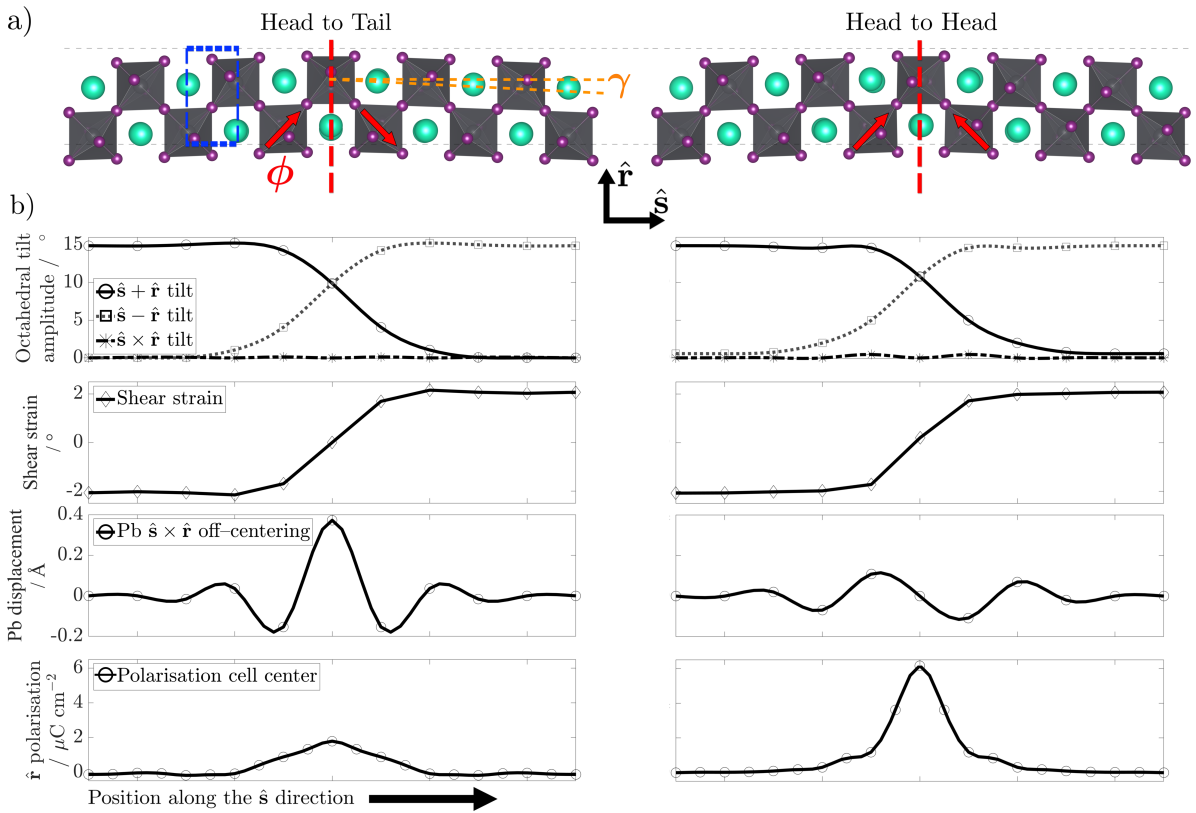
The twins characterised by Rothmann et al. Rothmann et al. (2017) are planar interfaces joining two domains whose tilt axes meet at . Figure 2a) shows two atomic structures consistent with these observed twins. Directions perpendicular and parallel to the planar interface are labelled by unit vectors and respectively. In fact, it can be shown that these are the only mechanically compatible twins ITD i.e. interfaces that do not introduce additional strains and stresses to this system. Both twins in Fig. 2 may be characterised by the relative orientation of tilt pseudovectors across the wall’s center. Following standard terminology Schiaffino and Stengel (2017), these are called ‘head to tail’ (HT) or ‘head to head’ (HH).
The twins were simulated with periodic boundary conditions in VASP 5.4.4 using the PBEsol exchange-correlation functional Perdew et al. (2008). Valence electron configurations 6s1, 6s26p2 and 5s25p5 were employed for Cs, Pb and I respectively with the supplied Projector-Augmented-Wave pseudopotentials generated in 2002 Blöchl (1994); Kresse and Joubert (1999); Kresse and Hafner (1993); Kresse and Furthmüller (1996). We used supercells containing 200 atoms, the centers of which are shown in Fig. 2a), such that the cell contained two walls (one at the center and another shared at the edges) yet was sufficiently large to recover the bulk properties between both walls. With an energy cutoff of 500 eV for the plane-wave basis and a Monkhorst-Pack grid Monkhorst and Pack (1976), both supercells were relaxed such that the maximum force on any atom is less than 10 meV Å-1.
III Results & discussion
 |
 |
We determined the formation energies of the twin boundaries to be and for the HT and HH walls respectively wal . The negative HH formation energy was found to arise from the octahedral tilt pattern across the wall. Between both single antiphase tilt I4/mcm domains, there is an intermediary structure characterised by two antiphase axes of different tilt amplitudes (cf. Fig. 2). This phase is of space group with Glazer notation . Unusually, the phase was found to be more stable than in our PBEsol calculations, which correspond to the limit of 0 K. We arrived at the same conclusion using the PBE functional and for different APbX3 chemistries where A = Fr, Rb and X = I, F. Nonetheless, these are small formation energies. Hence, as has been observed experimentally Rothmann et al. (2017); Liu et al. (2018b, c), we expect these walls to appear frequently.
The wall thicknesses were extracted from the change in octahedral tilts across the wall. Figure 2 shows plots of the magnitude of the cubic tilt vectors with respect to position along the direction. Fitting a hyperbolic tangent function ITD , where , and correspond to the bulk tilt amplitude, position along and the fitting parameter respectively, yields thicknesses of for both walls, indicating that they are thin. For comparison, in the prototypical oxide perovskite SrTiO3, the same wall geometries were calculated to have much larger thicknesses of Schiaffino and Stengel (2017). Our results imply that any emergent phenomena at the walls could be highly localised. Furthermore, these boundaries are likely to be relatively immobile in response to an external stress Tagantsev et al. (2010), which would help prevent wall annihilation.
We found both ferroelastic twins to be polar; a result that has not been discussed in their observation Rothmann et al. (2017); Liu et al. (2018b, c, a); Röhm et al. (2017); Strelcov et al. (2017); MacDonald et al. (2017); Hermes et al. (2016). The layer-by-layer polarisation was determined using Born effective charges computed in the centrosymmetric structure BEC . The and components were antipolar and hence contributed no net polarisation across the wall. Conversely, the component of is plotted in Fig. 2, yielding a relatively large net polarisation peaking at in the HT and HH walls respectively. The same domain wall geometries in SrTiO3 have been calculated to yield polarisations up to Schiaffino and Stengel (2017). We found this to be signficantly driven by Cs-cation off-centering in the HH wall, as opposed to that in the HT wall where the main contrbiution is from the larger Pb-cation Born effective charge. In the hybrid organic-inorganic system, we might expect the dipole moment of MA to enhance this contribution to the polarisation.
Furthermore, we note that ferroelastic boundaries are necessarily polar ITD . One may understand this as the juxtaposition of strain sates from both domains introducing a strain gradient across the wall. This necessarily induces a flexoelectric effect (a coupling between strain gradient and electric polarisation) that breaks inversion symmetry Schiaffino and Stengel (2017). One may estimate this coupling to be particularly pronounced in these walls as shown in Fig. 2b) by the large gradient in shear strain. It can be shown that the emergent polarisation at the wall is in-plane, corresponding to the direction in these HH and HT twins as confirmed by our results.
Although these walls are polar, this is only a necessary but not sufficient condition for ferroelectricity. To shed some light on this issue, we note that Schiaffino and Stengel have derived a Landau-like expansion of the potential energy landscape for the same wall geometries Schiaffino and Stengel (2017). They identified three ‘improper’ terms that are linear in and arise due to the walls’ structure. These terms describe couplings of with strain gradients (‘flexoelectric’), tilts and tilt gradients (‘rotopolar’) in addition to a term coupling with anti-polar B-cation off-centerings and tilts. These tilt, shear strain and Pb displacement profiles are plotted in Fig. 2. For an improper term to remain invariant under reversal, the sign of precisely one of the other terms in the coupling must also change. Due to the wall geometry, that appears unlikely to be possible and hence we would not expect this improper polarisation to be switchable. However, from computing phonon modes of the intermediate two (anti-phase) tilt system at the wall, we found this phase to contain an unstable polar mode. This indicates a double well polarisation for CsPbI3, even after normalisation with the competitive bi-quadratic coupling term from the tilts, and hence the possibility of an additional proper and switchable component to the polarisation. It is possible that a combination of these proper and improper polarisations may allow for the walls to be ferroelectric through the presence of multiple metastable polar states. Nonetheless, we note that the aforementioned flexoelectricity and the photoferroic effect could play an important role in the photovoltaic performance of HOIPs, irrespective of whether or not is switchable Yang et al. (2018). The notion that strain and strain gradients bring about such effects in MAPI has been hypothesised Tsai et al. (2018); Jones et al. (2018) and, in addition to the characterisation of these twins, Liu et al. Liu et al. (2018c, b) have imaged ionic segregation across the twin boundary which they attribute to the variation of strain.
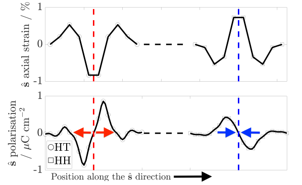
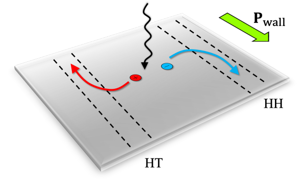
Figure 3 shows an estimate for axial strain perpendicular to the wall lay and the out-of-plane components of as a function of distance along the direction. The character of these polarisation components at the interface suggests that the HT and HH walls act as hole and electron sinks respectively. We propose that this implies the interfaces to be pathways that could enhance electron/hole mobility. Upon photoexcitation, an electron-hole pair may be separated into walls that act as their respective sinks, confining the charge carriers to the boundary and delaying recombination. The in-plane wall polarisations then would enhance electron/hole mobility along the walls, similar to the ferroelectric highways depicted by Frost et al. Frost et al. (2014). We have considered configurations where adjacent walls have parallel polarisation although antiparallel configurations are possible Schiaffino and Stengel (2017). In these ferroelastic twins, their experimental observation Rothmann et al. (2017) shows these walls to span over large distances and be a bulk phenomenon which may further support the proposed mechanism.
From the projected density of states we found the band gap at the walls and in bulk to be largely similar. However, in general this may be an additional effect at different types of domain walls, which will be a point of future investigation.
IV Conclusions
In this article, we have presented an ab initio study of ferroelastic CsPbI3 twins as a model for the same defects observed in MAPI. Both types of twins, HH and HT, were found to have a low formation energy, small thickness and a sizeable in-plane polarisation of despite separating non-polar domains. Potential avenues for enhancing photovoltaic performance via domain wall engineering have been discussed with a mechanism proposed for delaying recombination rates and enhancing charge carrier mobility. We hope to motivate further investigation into these structures and their role in the performance of hybrid organic-inorganic halide perovskite solar cells.
Acknowledgements.
We are grateful for the computational resources provided by the Imperial College Research Computing Service and the UK Materials and Molecular Modelling Hub, which is partially funded by EPSRC (EP/P020194/1). This work has been supported by the EPSRC Centre for Doctoral Training on Theory and Simulation of Materials (TSM-CDT, grant ref. EP/L015579/1). J.Í. thanks the support of the Luxembourg National Research Fund (Grant FNR/C15/MS/10458889 NEWALLS). Structural schematics in Fig. 1 & 2 were generated using the visualisation software VESTA 3 Momma and Izumi (2011).References
- Rothmann et al. (2017) M. U. Rothmann, W. Li, Y. Zhu, U. Bach, L. Spiccia, J. Etheridge, and Y.-B. Cheng, Nat. Commun. 8, 14547 (2017).
- Kojima et al. (2009) A. Kojima, K. Teshima, Y. Shirai, and T. Miyasaka, J. Am. Chem. Soc. 131, 6050 (2009).
- (3) “Best Research Cell Efficiencies, NREL,” https://www.nrel.gov/pv/, Accessed: 3rd January 2019.
- Bhatt and Lee (2017) M. D. Bhatt and J. S. Lee, New J. Chem. 41, 10508 (2017).
- Huang et al. (2017) J. Huang, Y. Yuan, Y. Shao, and Y. Yan, Nat. Rev. Mater. 2, 17042 EP (2017).
- Fridkin (1979) V. M. Fridkin, Photoferroelectrics Springer Series in Solid State Sciences, Vol. 9 (Springer-Verlag, Berlin, 1979).
- Sturman and Fridkin (1992) P. J. Sturman and V. M. Fridkin, Photovoltaic and Photo-refractive Effects in Noncentrosymmetric Materials, Vol. 8 (CRC Press, 1992).
- Butler et al. (2015) K. T. Butler, J. M. Frost, and A. Walsh, Energy Environ. Sci. 8, 838 (2015).
- Frost et al. (2014) J. M. Frost, K. T. Butler, F. Brivio, C. H. Hendon, M. van Schilfgaarde, and A. Walsh, Nano Lett. 14, 2584 (2014).
- Kutes et al. (2014) Y. Kutes, L. Ye, Y. Zhou, S. Pang, B. D. Huey, and N. P. Padture, J. Phys. Chem. Lett. 5, 3335 (2014).
- Fan et al. (2015) Z. Fan, J. Xiao, K. Sun, L. Chen, Y. Hu, J. Ouyang, K. P. Ong, K. Zeng, and J. Wang, J. Phys. Chem. Lett. 6, 1155 (2015).
- G et al. (2016) S. G, P. Mahale, B. P. Kore, S. Mukherjee, M. S. Pavan, C. De, S. Ghara, A. Sundaresan, A. Pandey, T. N. Guru Row, and D. D. Sarma, J. Phys. Chem. Lett. 7, 2412 (2016).
- Kim et al. (2016) Y.-J. Kim, T.-V. Dang, H.-J. Choi, B.-J. Park, J.-H. Eom, H.-A. Song, D. Seol, Y. Kim, S.-H. Shin, J. Nah, and S.-G. Yoon, J. Mater. Chem. A 4, 756 (2016).
- Rakita et al. (2017) Y. Rakita, O. Bar-Elli, E. Meirzadeh, H. Kaslasi, Y. Peleg, G. Hodes, I. Lubomirsky, D. Oron, D. Ehre, and D. Cahen, Proc. Natl. Acad. Sci. U. S. A. 114, E5504 (2017).
- Hoque et al. (2016) M. N. F. Hoque, M. Yang, Z. Li, N. Islam, X. Pan, K. Zhu, and Z. Fan, ACS Energy Lett. 1, 142 (2016).
- Whalley et al. (2017) L. D. Whalley, J. M. Frost, Y.-K. Jung, and A. Walsh, J. Chem. Phys. 146, 220901 (2017).
- Liu et al. (2018a) W. Liu, Y. Liu, J. Wang, C. Wu, C. Liu, L. Xiao, Z. Chen, S. Wang, and Q. Gong, Crystals 8 (2018a).
- Shan and Saidi (2017) W. Shan and W. A. Saidi, J. Phys. Chem. Lett. 8, 5935 (2017).
- Yin et al. (2014) W.-J. Yin, T. Shi, and Y. Yan, Adv. Mater. 26, 4653 (2014).
- McKenna (2018) K. P. McKenna, ACS Energy Lett. 3, 2663 (2018).
- Guo et al. (2017) Y. Guo, Q. Wang, and W. A. Saidi, J. Phys. Chem. C 121, 1715 (2017).
- Yin et al. (2015) W.-J. Yin, H. Chen, T. Shi, S.-H. Wei, and Y. Yan, Adv. Electron. Mater. 1, 1500044 (2015).
- Liu et al. (2015) S. Liu, F. Zheng, N. Z. Koocher, H. Takenaka, F. Wang, and A. M. Rappe, J. Phys. Chem. Lett. 6, 693 (2015).
- (24) L. Chen, C. Paillard, H. J. Zhao, J. Íñiguez, Y. Yang, and L. Bellaiche, npj Comput. Mater. , 75.
- Bischak et al. (2015) C. G. Bischak, E. M. Sanehira, J. T. Precht, J. M. Luther, and N. S. Ginsberg, Nano Lett. 15, 4799 (2015).
- Liu et al. (2018b) Y. Liu, L. Collins, A. Belianinov, S. M. Neumayer, A. V. Ievlev, M. Ahmadi, K. Xiao, S. T. Retterer, S. Jesse, S. V. Kalinin, B. Hu, and O. S. Ovchinnikova, Appl. Phys. Lett. 113, 072102 (2018b).
- Liu et al. (2018c) Y. Liu, L. Collins, R. Proksch, S. Kim, B. R. Watson, B. Doughty, T. R. Calhoun, M. Ahmadi, A. V. Ievlev, S. Jesse, S. T. Retterer, A. Belianinov, K. Xiao, J. Huang, B. G. Sumpter, S. V. Kalinin, B. Hu, and O. S. Ovchinnikova, Nat. Mater. (2018c).
- (28) International Tables for Crystallography, Vol. D, Chap. 3, pp. 358–559.
- Lee et al. (2016) J.-H. Lee, N. C. Bristowe, J. H. Lee, S.-H. Lee, P. D. Bristowe, A. K. Cheetham, and H. M. Jang, Chem. Mater. 28, 4259 (2016).
- Brivio et al. (2013) F. Brivio, A. B. Walker, and A. Walsh, APL Mater. 1, 042111 (2013).
- Eperon et al. (2015) G. E. Eperon, G. M. Paternò, R. J. Sutton, A. Zampetti, A. A. Haghighirad, F. Cacialli, and H. J. Snaith, J. Mater. Chem. A 3, 19688 (2015).
- Choi et al. (2014) H. Choi, J. Jeong, H.-B. Kim, S. Kim, B. Walker, G.-H. Kim, and J. Y. Kim, Nano Energy 7, 80 (2014).
- Weller et al. (2015) M. T. Weller, O. J. Weber, P. F. Henry, A. M. Di Pumpo, and T. C. Hansen, Chem. Commun. 51, 4180 (2015).
- Glazer (1972) A. M. Glazer, Acta Crystallogr., Sect. B: Struct. Sci., Cryst. Eng. Mater. 28, 3384 (1972).
- Schiaffino and Stengel (2017) A. Schiaffino and M. Stengel, Phys. Rev. Lett. 119, 137601 (2017).
- Perdew et al. (2008) J. P. Perdew, A. Ruzsinszky, G. I. Csonka, O. A. Vydrov, G. E. Scuseria, L. A. Constantin, X. Zhou, and K. Burke, Phys. Rev. Lett. 100, 136406 (2008).
- Blöchl (1994) P. E. Blöchl, Phys. Rev. B 50, 17953 (1994).
- Kresse and Joubert (1999) G. Kresse and D. Joubert, Phys. Rev. B 59, 1758 (1999).
- Kresse and Hafner (1993) G. Kresse and J. Hafner, Phys. Rev. B 47, 558 (1993).
- Kresse and Furthmüller (1996) G. Kresse and J. Furthmüller, Comput. Mater. Sci. 6, 15 (1996).
- Monkhorst and Pack (1976) H. J. Monkhorst and J. D. Pack, Phys. Rev. B 13, 5188 (1976).
-
(42)
We define the wall formation energy,
as
where and are the 200 atom wall cell and 20 atom conventional cells energies respectively and is the wall area contained in the supercell. The factor of accounts for the two walls in the supercell . - Tagantsev et al. (2010) A. Tagantsev, L. E. Cross, and J. Fousek, Domain in Ferroic Crystals and Thin Films (Springer-Verlag New York, 2010).
- Röhm et al. (2017) H. Röhm, T. Leonhard, M. J. Hoffmann, and A. Colsmann, Energy Environ. Sci. 10, 950 (2017).
- Strelcov et al. (2017) E. Strelcov, Q. Dong, T. Li, J. Chae, Y. Shao, Y. Deng, A. Gruverman, J. Huang, and A. Centrone, Sci. Adv. 3 (2017).
- MacDonald et al. (2017) G. A. MacDonald, C. M. Heveran, M. Yang, D. Moore, K. Zhu, V. L. Ferguson, J. P. Killgore, and F. W. DelRio, ACS Appl. Mater. Interfaces 9, 33565 (2017).
- Hermes et al. (2016) I. M. Hermes, S. A. Bretschneider, V. W. Bergmann, D. Li, A. Klasen, J. Mars, W. Tremel, F. Laquai, H.-J. Butt, M. Mezger, R. Berger, B. J. Rodriguez, and S. A. L. Weber, J. Phys. Chem. C 120, 5724 (2016).
-
(48)
We calculated the layer by layer
polarisation with Born Effective Charges such that
where and denote the Born Effective Charge and displacement from a reference high symmetry position of the th ion. Weights scale the contributions of ions shared with neighbouring cells that lie on the edges or vertices of the volume (e.g. an ion lying on a face–center is shared between two cells and hence ). The sum runs over all atoms contained in the volume in which the polarisation is computed . - Yang et al. (2018) M.-M. Yang, D. J. Kim, and M. Alexe, Science (2018).
- Tsai et al. (2018) H. Tsai, R. Asadpour, J.-C. Blancon, C. C. Stoumpos, O. Durand, J. W. Strzalka, B. Chen, R. Verduzco, P. M. Ajayan, S. Tretiak, J. Even, M. A. Alam, M. G. Kanatzidis, W. Nie, and A. D. Mohite, Science 360, 67 (2018).
- Jones et al. (2018) T. W. Jones, A. Osherov, M. Alsari, M. Sponseller, B. C. Duck, Y.-K. Jung, C. Settens, F. Niroui, R. Brenes, C. V. Stan, et al., arXiv preprint arXiv:1803.01192 (2018).
- (52) Axial strain was estimated by the expansion/compression of perpendicular distances between Cs–Pb–I planes relative to such a distance in the wall super cell where the bulk properties were recovered. Layer widths were calculated from taking distances between average positions of Cs and Pb cations in a given plane; these approximately correspond to the width of the dotted blue box along in Fig. 2a) .
- Momma and Izumi (2011) K. Momma and F. Izumi, J. Appl. Crystallogr. 44, 1272 (2011).