ab-initio calculation of band alignments for opto-electronic simulations
Abstract
A modified core-to-valence band maximum approach is applied to calculate band offsets of strained III/V semiconductor hetero junctions. The method is used for the analysis of (In,Ga)As/GaAs/Ga(As,Sb) multi-quantum well structures. The obtained offsets and the resulting bandstructure are used as input for the microscopic calculation of photoluminescence spectra yielding very good agreement with recent experimental results.
I Introduction
Semiconductor hetero structures are the basic building blocks of many opto-electronic devices, such as solar cells, semiconductor sensors, or laser diodes. By choosing appropriate alloys and layer structures, device makers have great flexibility in engineering the optical and electronic properties to meet their requirements. However, the parameter space for designing such structures is too large for simple experimental trial-and-error. It is therefore necessary to thoroughly understand the physics of these devices, and to be able to predict their performance with accurate simulation methods.
One fundamental requirement for the reliable prediction of the opto-electronic semiconductor hetero structure properties is a detailed knowledge of the electronic band structure throughout the device Haug and Koch (2009). Because energy bands are a property of the infinite system, complex layered hetero structures cannot be modeled directly using standard first principles approaches. Instead, one typically uses the so-called envelope function approximation where one keeps the bandstructure of the infinite bulk materials in the plane of the layers and accounts for the finite thickness in growth direction such that the hetero structure can be approximated by stacking these layers on top of each other Winkler and Rössler (1993). The infinite band structures of the reference bulk systems are then modified to take into account lattice strain imposed by the substrate, and quantum confinement arising from finite layer thicknesses.
In a second step, the bands of adjacent layers are connected at the structure interfaces, leading to the devices’ position-dependent overall band structure. The critical parameter required to connect the band structures at an interface is the relative energy offset of their valence band maxima (VBMs), the valence band offset (VBO) Franciosi and Van De Walle (1996). It determines both, transport across the interface as well as quantum confinement of the layers, making it one of the most important parameters for the design of hetero structures.
Estimations of the band alignment at semiconductor interfaces from first principles band structure calculations have a long history with various different suggested methods Tersoff (1984); Wei and Zunger (1998); Van De Walle (2006); Komsa et al. (2008). The state of the art is to combine calculations of bulk-like properties of the constituents with information about the interface. This typically requires performing at least three separate calculations (bulk material , bulk material , interface ) but has the advantage of yielding the true bulk-like VBO with manageable computational effort Komsa et al. (2008).
In this paper, we use the core-to-VBM method introduced by Wei and Zunger Wei and Zunger (1998), modified to take into account anisotropic strain in the grown layers as well as the exact chemical environment of the core levels in multinary materials. We show that the method can be used to construct the electronic band structure across a hetero junction. The results are then used as input into a microscopic theory allowing us to predict optical properties of the device.
In section II we describe the modified core-to-VBM method applied for the calculation of the VBO. We test the method for the example of the well-known GaAs/(Al,Ga)As interface in section III. In section IV, we then determine the band alignments of the hetero junctions GaAs/Ga(As,Sb) and GaAs/(In,Ga)As. We use the resulting band structure as input into the microscopic calculation of the photoluminescence spectra of these systems which are currently under investigation for use in flexible type II semiconductor lasers Fuchs et al. (2018). The work is concluded in section V.
II The modified core-to-VBM approach
The VBO of an interface between two materials and is defined as the VBM energy difference of the layers,
| (1) |
It is possible to extract and from a single first-principles density functional theory (DFT) calculation by calculating the position dependent VBM (one value for each side and of the interface), which can be done for instance by analyzing the localized density of states (LDOS) Bass, Oloumi, and Matthai (1989). However, such techniques introduce additional adjustable parameters and are relatively unprecise such that other approaches are usually preferred.
A more precise method is to compare the VBMs and of two separate calculations, one for each of the bulk materials and . Comparing the and from separate bulk calculations has the advantage of yielding the true bulk-like band offset, as information about the interface is not included in the electronic structure calculations. In addition, the calculation of and is much less involved, as the separate cells are smaller and finite size effects are less pronounced than in the interface-containing cell.
However, since the average electrostatic potential in infinite solids is an ill-defined quantity Balderschi, Baroni, and Resta (1988), a common energy reference level in both systems is required to align their energy scales before can be evaluated. Figure 1 a) and b) show the two bulk cells and , their schematic band structure around the -point, and some arbitrary reference level and (blue, dashed lines). The energy scales of the two cells are misaligned by an offset . The problem of calculating the VBO at the interface therefore reduces to aligning the energy scales between the and calculations, i.e., determining .
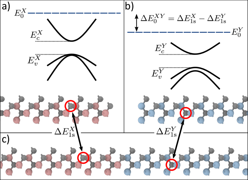
In the core-to-VBM approach, ionic core levels and provide the required reference energies Wei and Zunger (1998). These electronic states are sufficiently localized around the atomic cores not to be affected by “distant” structural features such as hetero interfaces. They do, however, depend on the chemical surrounding of their host ion, as well as the deformation potentials induced by lattice strain. For instance, the 1s core state of an As atom in GaAs is different to that of As atoms in AlAs. In multinary and strained materials, it becomes even more complicated as the core levels of any ion will depend on the exact chemical environment (distribution of atoms) and lattice parameters (strain and local static atomic displacements). It is therefore not possible to directly compare the core states of of the separate and calculations. Fortunately, unlike the VBMs and , core levels are not a bulk property but by nature very localized to their host ions, which makes it possible to calculate them in a single interface calculation without loss of precision.
The cell is constructed by stacking and on top of each other, thereby simulating a perfectly abrupt interface between the two bulk cells. Consequently, each atom in the bulk cells and has an image in the cell with the exact same chemical surrounding (apart from ions very close to the interface) and similar static atomic displacements, i.e., deformation potentials. Figure 1 c) shows the combined supercell and highlights example atoms in the individual bulk cells and their corresponding images in the cell (red circles).
The energy scales of and are then aligned as follows: Some core level is calculated for all ions in the bulk cells and and in the interface cell . A natural choice is the atomic 1s orbital, as it’s radius is the smallest and it is conveniently symmetric. The corresponding energy levels are then and for the ions in the and cell, and their images , in the interface cell.
Because
| (2) |
the energy offsets and between each bulk cell and the interface cell are found. The VBO then is:
| (3) |
It should be noted that in order to preserve the lattice strain and static atomic displacements in the interface cell with respect to the two bulk calculations and , all three calculations need to be structurally relaxed before the calculation of the core states and the valence band maxima. In semiconductor hetero structures, the lattice parameters perpendicular to the growth direction are usually equal to the substrate lattice constant, and the layers are free to expand or shrink only in growth direction. This should be taken into account when applying the core-level-to-VBM approach.
III The GaAs/(Al,Ga)As interface
To test the accuracy of the modified core-to-VBM method, we apply it to the GaAs/(Alx,Ga1-x)As hetero junction with varying composition x. Note, that throughout the paper, we study [001] growth direction and the corresponding interfaces. The (Al,Ga)As supercells are constructed using special quasi-random structure (SQS) Van de Walle, Asta, and Ceder (2002) to approximate infinite bulk alloys. The 1s core levels of the ions are calculated using the initial state approximation Köhler and Kresse (2004) and the VBOs were found by determining the highest occupied energy state in the bulk cells, and . Even though AlAs and GaAs have very similar lattice parameters, strain in the (Al,Ga)As cell was still taken into account by constraining the lattice constant parallel to the interface ( and direction) to that of GaAs (), and relaxing the cell in direction.
Let us briefly summarize the core-to-VBM method described in section II by the GaAs/(Al,Ga)As example.
-
1.
Construct the GaAs and (Al,Ga)As bulk cells with the GaAs lattice constant. Random distribution of Al and Ga atoms in the (Al,Ga)As cell is done by constructing SQSs van de Walle (2009).
-
2.
Relax the bulk cells in (001) growth direction to account for strain.
-
3.
Run electronic structure calculations of the bulk cells to determine and , as well as the 1s core levels and .
-
4.
Stack the relaxed bulk cells vertically ([001] direction) to construct the GaAs/(Al,Ga)As interface cell.
-
5.
Relax the interface cell. This is done to take into account corrections of the atomic structure at the interface.
- 6.
For the DFT calculations, we use the pseudo-potential based Vienna Ab initio Simulation Package Kresse and Furthmüller (1996) with the PBEsol exchange-correlation functional. Perdew et al. (2008) Spin-orbit coupling is not taken into account for the electronic structure calculations of GaAs and (Al,Ga)As, as it has negligible effect on the position of the VBMs in these materials Komsa et al. (2008). The size of the GaAs cell is cubic unit cells and we use a -centered Monkhorst-Pack Monkhorst and Pack (1976) k-point grid of . The (Al,Ga)As cell size is unit cells big (the long dimension is the growth direction) and a k-point grid of is used. For the calculation of the GaAs/(Al,Ga)As interface cell a k-point grid is used. The kinetic energy cut-off is in all calculations.
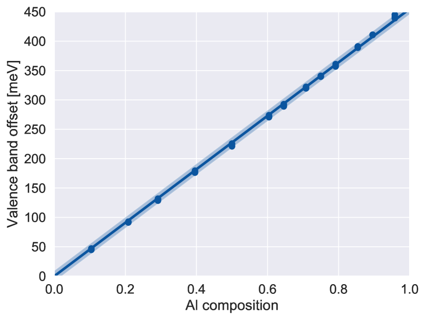
First, we study the VBO between GaAs and (Alx,Ga1-x)As depending on Al concentration x, which was varied between and . For each composition, five SQS configurations of atom placement on the group III sublattice (Al and Ga) were calculated to estimate the impact different lattice realizations. The results are shown in fig. 2. We obtain a linear dependence of
| (4) |
Our result aligns well with previous literature values, all of which are in the range for the GaAs/AlAs interface Vurgaftman, Meyer, and Ram-Mohan (2001); Wei and Zunger (1998); Wang and Stern (1985). A linear dependence of the offset on Al concentration has also been found previously Wang and Stern (1985). The uncertainty related to the distribution of Al and Ga atoms in the (Al,Ga)As cell is .
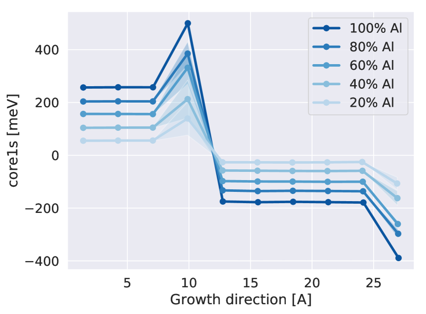
The position dependence of the 1s core states of As atoms throughout the supercell is shown in fig. 3. For each As (group III) layer in the hetero structure, the difference between the 1s core levels of the interface cell and of the bulk reference cell is shown. The energies are averaged over all As atoms in the layer. We can make two observations from the data. First, the core levels clearly converge to their bulk values within not more than two atomic layers distance from the interface. This shows that the interface has negligible effect on the core levels and that the core-to-VBM method described in section II requires not very extended cells in growth direction. Second, the relative core levels are constant in the respective parts of the cell, which indicates that they are not influenced by long-range electric fields, such as a macroscopic polarizations.Bernardini and Fiorentini (1998)
Our results for the GaAs/(Al,Ga)As model system are encouraging and suggest that the method can readily be applied to other semiconductor hetero junctions. In the next section, we study the GaAs/Ga(As,Sb) and GaAs/(Ga,In)As interfaces, which are highly relevant for the construction of flexible type-II semiconductor lasers.
IV GaAs/Ga(As,Sb)/(Ga,In)As MQW structures
The core-to-VBM method is applied to the GaAs/(In,Ga)As and GaAs/Ga(As,Sb) hetero interfaces. These materials are currently investigated for use in type II semiconductor lasers. Fuchs et al. (2018) The results are used to calculate photoluminescence (PL) spectra for an (In,Ga)As/GaAs/Ga(As,Sb) multi quantum well (MQW) structure, and are compared with experimental data from Ref. Gies et al., 2016.
IV.1 Band offsets
The details of the calculations are the same as for the GaAs/(Al,Ga)As interface: Realizations of atomic placements are generated using SQS, the GaAs cell size is cubic unit cells and the (In,Ga)As and Ga(As,Sb) cells are unit cells big, with similar k-point grids as described in section III. In all electronic structure calculations spin-orbit coupling is taken into account, as it has significant effect in In and Sb containing materials.
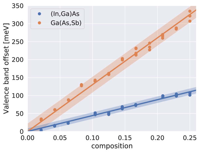
For both interfaces, we study the dependence of the VBO on concentration of the dilute constituents (In and Sb). The results are shown in fig. 4. Clearly, the VBOs depend not only on the concentration of In or Sb, but vary also with atomic placement. In the studied composition range of , which covers the materials relevant for applications, the dependence of the offsets on concentration is linear. The data yields the following results for the composition-dependent VBOs:
| (5) |
With the results from eq. 5 the (In,Ga)As/GaAs/Ga(As,Sb) MQW structure can be constructed. The modeled structure is shown schematically in the inset of fig. 5. Table 1 lists the parameters for the different quantum wells, with compositions and thicknesses taken (within experimental uncertainty) from the study Ref. Gies et al., 2016. The band gaps in Table 1 are calculated using values from Ref. Vurgaftman, Meyer, and Ram-Mohan, 2001. For the calculation of the VBOs the core-to-VBM method, detailed above, is used.
| Thickness | Band gap | Conc. | VBO | |
|---|---|---|---|---|
| (In,Ga)As | In | |||
| Ga(As,Sb) | Sb | |||
| GaAs |
IV.2 Photoluminescence
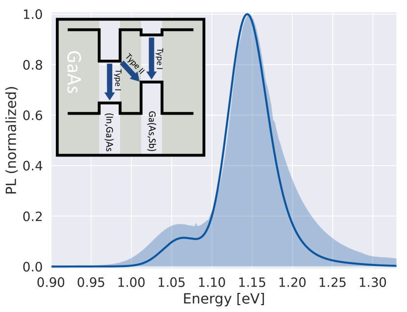
Experimentally measured PL spectra for GaAs/Ga(As,Sb)/(Ga,In)As MQW structures have been presented in Ref. Gies et al., 2016. A typical example is reproduced as the shaded area in Fig. fig. 5. In the figure, we clearly see the type I transition of the Ga(As,Sb) quantum well around and the type II transition between the (In,Ga)As and Ga(As,Sb) quantum wells appears at , respectively. For more details on the transition assignment, the sample used, and the measurement techniques, we refer the interested reader to Ref. Gies et al., 2016.
In our microscopic calculations of the PL spectrum, we solve the semiconductor luminescence equations Kira et al. (1999). Here, we assume equilibrium Fermi-Dirac distributions for the excited electron-hole pairs. The Coulomb matrix elements, the dipole matrix elements, and the single particle energies are calculated using 88 kp theory Hader, Linder, and Döhler (1997); Chow, Koch, and Sargent (1994). The electron-electron and electron-phonon scattering is taken into account at the level of the second-Born-Markov approximation Hader, Koch, and Moloney (2003). The spectrum is inhomogeneously broadened by convolution with a FWHM Gaussian distribution in order to take structural disorder effects into account.
The computed PL spectrum is shown as solid line in fig. 5. The comparison with the experimental results yields good overall agreement. In particular, both the type I and the type II transitions are reproduced rather well, confirming that the computed band offsets are close to the experimentally realized values.
V Conclusion
In this paper we show how the core-to-VBM method, modified to include anisotropic strain and static atomic displacements (SADs), can be used to accurately predict VBOs of III/V semiconductor hetero junctions. The method is first applied to the well-known GaAs/(Al,Ga)As interface and compares well with results from the literature. As expected, a linear dependence of the offset on Al concentration is found, with the GaAs/AlAs offset at .
In section IV, the approach is applied to the (In,Ga)As/GaAs/Ga(As,Sb) MQW, which is currently investigated for flexible type II semiconductor lasers. Within the compositional uncertainty and for the region of interest of we find linear dependencies of the GaAs/(In,Ga)As and GaAs/Ga(As,Sb) VBOs on In and Sb concentration, respectively. The calculated offsets are used to predict the PL spectrum for an MQW hetero structure, which is compared with experimental measurements from Ref. Gies et al., 2016. The type II transition energy is well reproduced, indicating successful prediction of the offsets.
Our results show that the core-to-VBM method is suitable to predict band alignments of strained semiconductor hetero junctions from first principles and can readily be applied to other material systems. In conjunction with solvers for optical properties, it is possible to calculate quantities such as PL spectra without experimental input, allowing to theoretically design and tune functionalized semiconductor hetero structures prior to growth. By fitting to experimental measurements, such a combined approach can also be used to gain insight into structural or electronic properties of samples.
VI Acknowledgements
Financial support is provided by the German Research Foundation (DFG) in the framework of the GRK 1782 and SFB 1083.
References
- Haug and Koch (2009) H. Haug and S. W. Koch, Quantum Theory of the Optical and Electronic Properties of Semiconductors, 5th ed. (World Scientific, 2009).
- Winkler and Rössler (1993) R. Winkler and U. Rössler, Physical Review B 48, 8918 (1993).
- Franciosi and Van De Walle (1996) A. Franciosi and C. G. Van De Walle, Surface Science Reports 25, 1 (1996).
- Tersoff (1984) J. Tersoff, Physical Review B 30, 4874 (1984).
- Wei and Zunger (1998) S. H. Wei and A. Zunger, Applied Physics Letters 72, 2011 (1998).
- Van De Walle (2006) C. G. Van De Walle, Physica B: Condensed Matter 376-377, 1 (2006).
- Komsa et al. (2008) H.-P. Komsa, E. Arola, E. Larkins, and T. T. Rantala, Journal of Physics: Condensed Matter 20, 315004 (2008).
- Fuchs et al. (2018) C. Fuchs, A. Brüggemann, M. J. Weseloh, C. Berger, C. Möller, S. Reinhard, J. Hader, J. V. Moloney, A. Bäumner, S. W. Koch, and W. Stolz, Scientific Reports 8, 8 (2018).
- Bass, Oloumi, and Matthai (1989) J. M. Bass, M. Oloumi, and C. C. Matthai, Journal of Physics: Condensed Matter 1, 10625 (1989).
- Balderschi, Baroni, and Resta (1988) A. Balderschi, S. Baroni, and R. Resta, Physical Review Letters 61, 734 (1988).
- Van de Walle, Asta, and Ceder (2002) A. Van de Walle, M. Asta, and G. Ceder, Calphad: Computer Coupling of Phase Diagrams and Thermochemistry 26, 539 (2002).
- Köhler and Kresse (2004) L. Köhler and G. Kresse, Physical Review B 70, 165405 (2004).
- van de Walle (2009) A. van de Walle, Calphad: Computer Coupling of Phase Diagrams and Thermochemistry 33, 266 (2009).
- Kresse and Furthmüller (1996) G. Kresse and J. Furthmüller, Physical Review B: Condensed Matter and Materials Physics 54, 11169 (1996).
- Perdew et al. (2008) J. P. Perdew, A. Ruzsinszky, G. I. Csonka, O. A. Vydrov, G. E. Scuseria, L. A. Constantin, X. Zhou, and K. Burke, Phys. Rev. Lett. 100, 136406 (2008).
- Monkhorst and Pack (1976) H. J. Monkhorst and J. D. Pack, Physical Review B 13, 5188 (1976).
- Vurgaftman, Meyer, and Ram-Mohan (2001) I. Vurgaftman, J. R. Meyer, and L. R. Ram-Mohan, Journal of Applied Physics 89, 5815 (2001).
- Wang and Stern (1985) W. I. Wang and F. Stern, Journal of Vacuum Science & Technology B 3, 1280 (1985).
- Bernardini and Fiorentini (1998) F. Bernardini and V. Fiorentini, Physical Review B - Condensed Matter and Materials Physics 57, R9427 (1998).
- Gies et al. (2016) S. Gies, M. J. Weseloh, C. Fuchs, W. Stolz, J. Hader, J. V. Moloney, S. W. Koch, and W. Heimbrodt, Journal of Applied Physics 120, 204303 (2016).
- Kira et al. (1999) M. Kira, F. Jahnke, W. Hoyer, and S. W. Koch, Progress in Quantum Electronics 23, 189 (1999).
- Hader, Linder, and Döhler (1997) J. Hader, N. Linder, and G. H. Döhler, Physical Review B 55, 6960 (1997).
- Chow, Koch, and Sargent (1994) W. W. Chow, S. W. Koch, and M. Sargent, Semiconductor-Laser Physics (Springer Berlin Heidelberg, 1994).
- Hader, Koch, and Moloney (2003) J. Hader, S. Koch, and J. V. Moloney, Solid-State Electron. 47, 513 (2003).