Engineering Topological quantum dot through planar magnetization in bismuthene
Abstract
The discovery of quantum spin Hall materials with huge bulk gaps in experiment, such as bismuthene, provides a versatile platform for topological devices. We propose a topological quantum dot (QD) device in bismuthene ribbon in which two planar magnetization areas separate the sample into a QD and two leads. At zero temperature, peaks of differential conductance emerge, demonstrating the discrete energy levels from the confined topological edge states. The key parameters of the QD, the tunneling coupling strength with the leads and the discrete energy levels, can be controlled by the planar magnetization and the sample size. Specially, different from the conventional QD, we find that the angle between two planar magnetization orientations provides an effective way to manipulate the discrete energy levels. Combining the numerical calculation and the theoretical analysis, we identify that such manipulation originates from the unique quantum confinement effect of the topological edge states. Based on such mechanism, we find the spin transport properties of QDs can also be controlled.
pacs:
73.63.-b, 73.23.-b, 85.75.-dI Introduction
The Quantum spin Hall (QSH) effect with topological helical edge states is one of the focuses in the topological state studies CLKane ; CLKane1 ; BABernevig ; MKonig ; SQShen ; XLQi1 ; XLQi ; MZHasan . In the QSH systems, carriers can propagate without dissipation along the edge channels. At one edge, carriers of spin-up and spin-down flow to opposite directions. Specifically, the propagation direction of the carriers of the same spin is reversed at the opposite edge. Such unique transport properties enable QSH systems to own promising applications in low-power electronics and spintronicsYZhangKHe ; YFRen ; VSverdlovS ; PChen . In the early years, the studies of QSH systems mainly focus on group-VI monolayers (e.g., grapheneCLKane ; CLKane1 and siliceneCCLiu ; CCLiu2 ) and semiconductor quantum wells (e.g., HgTe/CdTeBABernevig ; MKonig and InAs/GaSbCXLiu ; IKnez ). However, the weak spin-orbit coupling of these systems only leads to a tiny bulk gap with the order of a few meV, which limits the applications in the topological devices. Recently, the QSH effect is proposed in group-V monolayers (e.g., bismuthene ZFWang ; CCLiu3 ; IKDrozdov ; XLi and antimonene ZGSong ; YDMa ; SGCheng ; MPumera ). In these systems, the bulk gap can reach the same order of the atomic spin-orbit coupling strength of Bi and Sb. Significantly, F. Reis et al. have synthesized the bismuthene sample on the SiC substrate, and they observed a large topological bulk gap up to eVFReis . The discovery generates extensive attentions in the QSH phase on group-V monolayers and the related applications in topological devices GLiWHanke ; JGouBYXia ; HQHuangFLiu . Furthermore, it is found that the topological characteristics of group-V monolayers can easily be modified by doping, adsorption, chemical modification or substrate effect WXJi ; SCChen ; SHKim ; AJMannix ; FYang ; LChen ; BTFu ; HGao ; THirahara ; THirahara1 . For example, the first-principles calculations have demonstrated that the magnetic doping or substrate can induce very large exchange fields (up to 400 meV) in the functionalized bismutheneTZhouJYZhang and antimonene TZhou ; TZhou1 , which drives the system from the QSH phase to quantum anomalous Hall and valley polarized QSH phases, respectively. This easily modified feature of group-V monolayer is favorable for building topological devices.
Quantum dot (QD) is one of the most important devices in mesoscopic physicsRHansonLP ; SMReimannM ; PFendleyAW ; PAMaksymT ; GBurkardDLoss ; JRPetta ; YAlhassid . Because of the promising application for quantum computation and quantum information, engineering QDs with topological states draws lots of interestAImamogluDD ; DLossDP ; GBurkard ; KChang ; PBonderson . A typical QD system is shown in Fig. 1(c), where the QD is separated from two leads by insulated barriers. The QD has discrete energy levels due to the finite-size effect, and thus carriers can pass through the QD by resonance tunneling. The techniques for fabricating traditional topological QDs depend on chemical etchingGTian ; GFulop or gate voltage depletionJRPetta ; YPSong . However, such techniques require precise micromachining process and the control is much difficult. To this end, novel approaches for QD engineering are expected. Due to the spin-momentum locked nature of helical edge states in the QSH phase, the planar magnetization opens a gap as large as the exchange field in the energy band of edge statesMKonigHBuhmann ; JLLadoJ ; DLWangZY ; XLQiTL . And recently, the QSH effect under local planar magnetization has been studied in monolayer systemsZLiuGZhao ; XTAn . It is found that the tunneling coupling between the separated sides is exponentially weakened by increasing the length of the magnetization areaXTAn . A natural question is whether we can take such an advantage of planar magnetization in group-V monolayers, which have the large topological bulk gap and highly tunable physical properties, to engineer topological QDs and manipulate their transport properties.
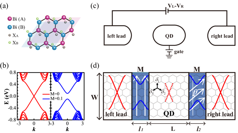
In this paper, we propose a QD in bismuthene nanoribbon by introducing two depletion regions with planar magnetization [as shown in Fig. 1(d)]. The coupling between the QD and the leads on both sides can be controlled by the magnetization. By varying the Fermi level, a series of peaks emerge in zero-temperature differential conductance, which comes from the discrete energy levels of the QD. We find the discrete energy levels originate from the quantum confinement of topological edge states and can still be observed even in a QD with a quite large size. Significantly, the angle between two planar magnetization orientations tunes the positions of discrete energy levels in the topological QD effectively. Through both numerical simulations and theoretical analysis, the unique confinement mechanism of the topological edge states is revealed. The magnetization-controlled discrete energy levels provide another way to manipulate the spin transport properties of the topological QD. Finally, both characteristics of electrical conductance and spin conductance of the QD device under finite bias are obtained.
The paper is organized as follows. Section II introduces the model of the topological QD and the numerical method to calculate the electrical and spin differential conductance. The key characteristics of the topological QD and its related transport properties are given in Sec. III. Then a brief conclusion is presented in Sec. IV.
II Model and methods
For convenience, we use zigzag bismuthene ribbons as a platform to demonstrate our proposal in detail. The topological QD device as illustrated in Fig. 1(d) is considered. Two planar magnetization areas (dark regions) separate the device into the QD and the contacting leads. The device can be described by the following HamiltonianTZhou :
| (1) |
Here, is the annihilation (creation) operators of electrons at site . and are the Pauli matrices acting in orbital [ and ] and spin space ( and ), respectively. The hopping describes the nearest hopping from site to , where is a constant and is the hopping coefficient. is the intrinsic spin-orbit coupling strength. refers to the planar exchange field in the sublattice, which originates from the adatoms . only acts on the planar magnetization regions and equals to zero in other regions. defines the orientation of planar magnetization, which can be controlled by the external magnetic field. Although it has not been observed in experiment yet, the proper adsorption (e.g., or ) can indeed induce large planar magnetization through the first-principle calculations. Detailed results are provided in the Appendixfootnote1 ; footnote2 .
To characterize the properties of the topological QD, the zero-temperature electrical differential conductance at the Fermi energy is calculated. Based on nonequilibrium Green’s function method and Landauer-Bttiker formulaSDatta , under a small bias can be expressed as:
| (2) |
where is the linewidth function of the leads () and is the retarded Green’s function SDatta . contains the Hamiltonian of the QD and two planar magnetization areas. The self-energy of the semi-infinite lead- can be calculated numericallyDHLee ; MPLopezSancho1 ; MPLopezSancho2 .
Since spin is a good quantum number in both leads, one can also calculate the spin differential conductances and . In analogy to Eq.(2), is obtained by
| (3) |
where . Here, are the corresponding spin part of .
III Results and Discussions
Before presenting our main results, the parameters adopted in the following studies are given. Here, eV, eV and eV, which are comparable to the fitting parameters of bismuthene from the first-principles data. The magnitude and the orientation angle of the exchange fields can be engineered by the atomic adsorption (e.g., concrete adatoms and their concentration) and the external magnetic field, respectively. For simplicity, we assume the atomic adsorptions are the same in two magnetization areas. Thus, the magnitude of exchange fields ( and ) are the same in two areas. Then, topological helical edge states exist in the low energy region . The exchange fields in the planar magnetization areas open a gap in the edge states [shown in the right panel of Fig. 1(b)], while its orientation does not change the band structure.
III.1 A versatile platform for building topological QD devices with tunable key parameters
We demonstrate our proposal through the simulations of transport properties. Transport performance is not only one of the most essential properties of QD devices, but also an effective method to characterize them. For example, for a non-interacting QD device, the tunneling coupling strength and the discrete energy levels are the key parameters. These parameters can be extracted from the zero-temperature two-terminal differential conductance:
| (4) |
where denotes the Fermi energy, denotes the discrete energy, labels the tunneling coupling strength between the QD and the left (right) leads HHaugAPJauho .
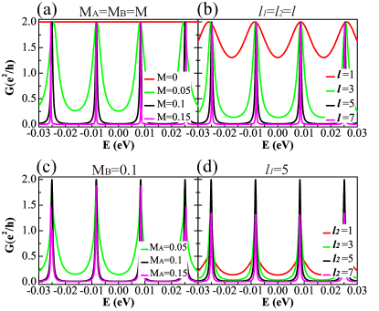
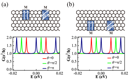
In Fig. 2(a) and 2(b), the linear differential conductance versus the Fermi energy under different exchange fields and lengths of the magnetization area are plotted. In the absence of planar magnetization (), indicates no QD is found in the device [see the red line in Fig. 2(a)]. However, when and , oscillates from to in the energy region , indicating the formation of the QD by introducing the two magnetization areas. The energies of peaks stand for the positions of the discrete energy levels. The sharpness of peaks represents the tunneling coupling strength between the QD and the leads. The physical picture for the QD is very intuitive. The planar magnetization can open a edge state gap by adding two barriers that locate on corresponding magnetization regions [see dark regions in Fig. 1(d)]. The electronic states inside the central region are confined to the discrete energy levels of the QD sample. Due to the finite width and height of the two barriers, the carriers can pass through the device by quantum tunneling. If the Fermi energy equals the discrete energy level , the resonance tunneling happens. Therefore, a proposal for building a QD device from a bismuthene nanoribbon is established.
The proposed QD device is a versatile platform. Its key parameters can be easily tuned. First, we show the feasibility to control the tunneling coupling strength and the related transport properties. Physically, the tunneling coupling strengths between the QD and two leads are determined by the probability of quantum tunneling across the planar magnetization regions. It can be changed by the exchange fields ( and ) and the lengths of the magnetization area ( and ). In Fig. 2(a) and 2(b), one can find that the oscillations are weak for small and [e.g., eV in Fig. 2(a), in Fig. 2(b)]. By increasing or , the tunneling coupling strength decays exponentially. shows clear oscillations from to and their peaks become narrow. For large and , the quantum tunneling from the leads to the QD is difficult. Correspondingly, the peaks of are too sharp to be observed [e.g., eV in Fig. 2(a), in Fig. 2(b)]. Besides, versus for and are also studied. In Fig. 2(c), by varying , the sharpness of is changed, while the maximum of its peaks nearly remains . In contrast, when , not only the sharpness of is changed, but also its peak maximums decreases from to [see Fig. 2(d)]. The reason is intuitively simple. As stated in Eq. (4), when , the tunneling coupling strength of two peaks are equal, i.e., . A peak of is obtained. While , one obtains a smaller resonant peak due to . For example, when and is nearly 14 times as , the resonant conductance gives .
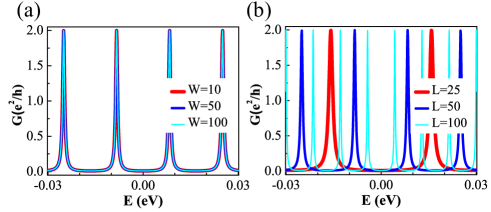
The discrete energy level is another key parameter of the QDs. In traditional QDs, the discrete energy levels are sensitive to its size. An increasing size always generates more discrete energy levels. In our proposal, the QD is built from a topological material. What are the differences between the traditional and our topological QD? In the following, we study it in detail. For better observation of the discrete energy levels, we use a symmetric model, ie., , and .
The differential conductance versus the Fermi energy for different ribbon widths and lengths are plotted Fig. 3. One can find that the conductance is not affected by as the curves of , and coincide with each other. It manifests that the discrete energy levels come from the quantum confinement of the topological edge states and the number of the discrete energy levels cannot be changed by the width of the QD. In contrast, the length can effectively manipulate the peaks of the conductance, i.e., discrete energy levels of the QD. As shown in Fig. 3(b), the increasing length induces more discrete energy levels. Further, the spacing of discrete energy levels is equal and inversely proportional to the length . This phenomenon is also consistent with the linear dispersion of topological edge states. The behaviors of versus both and not only prove that the discrete energy levels stem from the confinement of the topological edge states, but also demonstrate that the discrete energy levels can also be controlled.
It is worth noting that, different from the traditional QDs where discrete energy levels come from the confinement of bulk states, the absence of bulk states makes the spacing of discrete energy levels much larger in the present topological QD. For example, one can estimate from Fig. 3(b) that the level spacing is about 10 meV for the topological QD with size (). The immunity of discrete energy levels to the width makes the fabrication and the observation of the topological QDs in experiments more easily.
III.2 Manipulate the discrete energy levels by the angle of planar magnetization orientations
In the subsection III.1, we have proposed a topological QD device in the bismuthene nanoribbon. We demonstrate that its key parameters can be tuned by the barriers and the sample size. These characteristics also exist more or less in the traditional or other topological QD devices. Does any unique topological property exist in our topological QD? In this subsection, we show the discrete energy levels can be adjusted by the angle between two planar magnetization orientations.
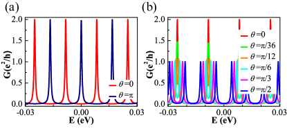
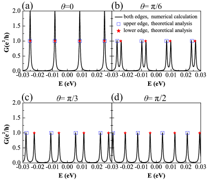
In Fig. 4, we study the behaviors of the differential conductance under different . Although the orientation of the exchange fields cannot change the insulating nature of the potential barriers, surprisingly, it can regulate the discrete energy levels of the QD. When two planar magnetization orientations change from being parallel () to being antiparallel (), the conductance peaks for appear in the middle of the neighbor conductance peaks for [see Fig. 4(a)]. In other words, the discrete energy levels shift a half period by reversing a planar magnetization orientation. This property may be used as a quantum bit with two states and , in which the transition condition is just reversing the magnetic field in one planar magnetization area. When the angle doesn’t equal to or , the linear conductance cannot reach . The peaks split and the amplitudes decrease from to when the angle increases from to . And the peaks will restore to gradually when changes from to . The former variation process is given in Fig. 4(b). In order to explain this phenomenon, we speculate that the factor originates from two edge states. The discrete energy levels, arising from the confinement of topological helical states at the upper or lower edge of the QD, contribute a conductance peak with an amplitude . And the angle shifts discrete energy levels to the opposite energy directions. In the following, two evidences are provided to support the argument.
The first evidence is given by the conductance simulation of two modified setups. As shown in Fig. 5, the exchange field is only introduced at one edge. When the exchange fields exist at the upper edge, the helical edge state at the lower edge are dissipationless and contributes to a quantized conductance . The confined states at the upper edge make the differential conductance oscillate between and . And the peaks of shift periodically with the angle . We plot the results of under , and find that the evenly spaced peaks shift leftwards [see the bottom panel of Fig. 5(a)]. When the exchange fields exist at the lower edge, the peaks of also oscillate from to . But the evenly spaced peaks of under shift rightwards. For and , the conductance peaks contributed by the upper edge and lower edge meet at the same energy positions. So has a oscillation from to if the exchange fields exist at the both edges. When deviates from those two specific angles, the degeneracy of discrete energy levels at the two edges are broken and each peak of splits into two. Thus, the amplitude of decreases from to [see Fig. 4(b)].
The second evidence is given by the theoretical analysis of the bound energies, i.e., discrete energy levels, at two edges. The proposed QD structure can be simplified as a one-dimensional finite potential well with a length and two semi-infinite barriers with the mass term . The upper edge states inside the potential well can be described by the Hamiltonian
| (5) |
Here, the operator and denotes the Fermi velocity. The eigenfunction in the range can be expressed as
| (6) |
with the bound energy .
In the left side, the barrier is and the Hamiltonian can be written as
| (7) |
Here, an evanescent wave with vector () exists in the barrier. The corresponding eigenfunction in the range is
| (8) |
In the right side, the barrier is and the Hamiltonian is
| (9) |
Here, the rightward evanescent wave vector is and the corresponding eigenfunction in the range is
| (10) |
According to the continuity condition , , we obtain the relationship for the bound energy at the upper edge, that is,
| (11) |
The lower edge states inside the potential well can be described by Hamiltonian
| (12) |
The potential in the two sides are still and . After some algebra, one can obtain the corresponding relationship for the bound energy at the lower edge:
| (13) |
A comparison of the numerical simulation and the theoretical analysis is given in Fig. 6. The numerical results are extracted from Fig. 4(b), and the analytical results are the solutions to the Eqs. (11) and (13). The discrete energy levels from the upper edge or the lower edge contribute a quantized conductance . So we label the solutions of the Eqs. (11) and (13) in the values of . In Fig. 6, all the labels of the solutions locate at the peaks of . Further, when two kinds of labels, i.e., bound energies at the two edges, coincide with each other [see Fig. 6(a)], peaks of emerge. If these two kinds of labels separate with each other [see Fig. 6(b-d)], the peaks of reduce from to and every solution is accompanied with a peak [see Fig. 6(b-d)]. Significantly, comparing four subplots with the increasing angle , one finds that the discrete energy levels contributed by the upper edge will move in a negative energy direction, while the discrete energy levels contributed by the lower edge will move in the positive energy direction.
The numerical simulation of differential conductance, the theoretical analysis of bound energies and the prefect coincidence of their results all confirm that the discrete energy levels can be manipulated by the angle between two planar magnetization orientations. From the theoretical analysis, such a manipulation requires: (1) the band structure with helical edge states; (2) the opposite propagation directions for spin carrier between the upper and the lower edges; (3) the special boundary condition induced by the exchange fields. All three characteristics are the essential properties of the QSH phase. Therefore, the manipulation by the angle is unique in the present proposed topological QD.
III.3 Application of unique manipulation mechanism by the angle of planar magnetization orientations
We have shown that the angle of the planar magnetization orientations introduces a special confinement mechanism to the topological edge states, leading to the unique manipulation of the discrete energy levels in the proposed QD. It is natural to ask whether we can utilize such mechanism for spintronics. As the bismuthene is a QSH material, the spin-up carriers will flow along the upper edge while the spin-down carriers flow along the lower edge under a small bias. Since the discrete energy levels at upper and lower edges move to different directions by tuning . Thus, such a manipulation may have applications in spintronics. We test the application by studying the spin differential conductance , and .
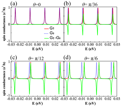
Figure 7 plots the variation of spin differential conductance , and with the Fermi energy . Both and oscillate from to in the proposed QD device. The peaks of and correspond to the discrete energy levels at the upper and lower edge, respectively. When two planar magnetization orientations are parallel (), and are identical and their variation is zero [see the blue line in Fig. 7(a)]. There is no spin current in the QD device. In contrast, by increasing , the peaks of and shift to the opposite energy directions, and consequently becomes nonzero. The current in the QD device becomes spin polarized. For a small [see Fig. 7(b) and 7(c)], the separation of the discrete energy levels coming from upper and lower edges is small, the peaks of are smaller than . This means both the upper and lower edges contribute a finite current, and the current is partially spin polarized. For a large [see Fig. 7(d)], and are well separated in energy. Thus, a pure spin current can be obtained in this case. Moreover, by tuning the Fermi energy , can be tuned from to . In other words, the current can be switched from pure spin-up polarization to pure spin-down polarization.
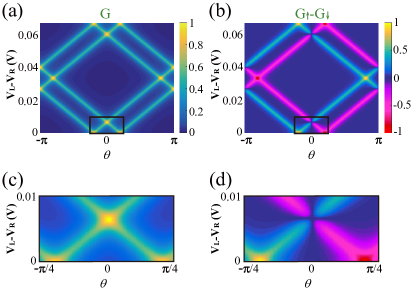
Next, we give another method to manipulate the spin polarized current other than by tuning the Fermi energy, as shown in Fig. 8. In a traditional QD, the transport properties are also tuned by a finite bias . Here, we set . In this case, the differential conductance and the spin differential conductance are modified to and , respectively. Figure 8 is obtained from these two formulas. The bias plays the similar role as the Fermi energy . By tuning , the resonant tunneling can also be observed in [see Fig. 8(a) and 8(c)]. shows a rapid oscillation by variation of both angle and finite bias , except or [see Fig. 8(b) and 8(d)]. Therefore, the unique manipulation of spin transport by the angle of planar magnetization orientations always holds.
From above studies, one can conclude that the spin transport properties of the proposed topological QD can be controlled by a new parameter, the angle between two planar magnetization orientations. Therefore, such unique manipulation mechanism has promising applications in spintronics.
IV Conclusion
In this paper, we select bismuthene as a candidate of our proposal. The most important reason is that bismthene is a QSH material with a large bulk gap and has been realized in experiments FReis . More recently, the QSH is also observed in with a bulk gap of eV JLCollinsA . Besides, lots of materials, such as staneneFFZhuWJChen ; YXuBYan and XFQianJWLiu ; YZhangTRChang , are predicted to host large bulk gap QSH effects. In principle, our proposed topological QD model can also be applied in these systems. To well observe the QD phenomena in experiments, the spacing of the discrete energy levels in QDs prefers one order smaller than the bulk gap. Because of the limited energy resolution, the distinction of discrete energy levels and the application of the topological QD device in small bulk gap QSH materials may be difficult.
In summary, we find a new method to engineer the topological QD system in bismuthene. The QD effect arises from the quantum confinement of the topological edge states by applying planar magnetizations. The coupling strength, the discrete energy levels and other key parameters of the QD can be controlled feasibly. Interestingly, different from the conventional QD, we find that the angle between two planar magnetization orientations can effectively tune the discrete energy levels of this topological QD. The phenomenon originates from the unique confinement mechanism of the topological edge states under different boundary conditions, caused by the variation of angle . Finally, we find the spin transport properties of the topological QD can also be manipulated by such a mechanism.
V ACKNOWLEDGMENTS
We thank Haiwen Liu, Qing-feng Sun, Zhi-min Yu and and Wen-Long You for helpful discussion. This work was supported by NSFC under Grants No. 11534001, 11822407, 11874298, 11574051 and 11874117, NSF of Jiangsu Province under Grants No. BK2016007. J.J. Zhou and T. Zhou contributed equally to this work.
VI Appendix
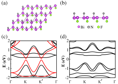
To observe the interesting phenomena in our proposal, we need a real material system described by the Hamiltonian Eq. (II). Based on first-principles calculations, we found the nitrogenated bismuth fluoride monolayer Bi2NF [shown in Fig. 9(a) and (b)] is a good material candidate for our proposal. The Bi2NF has a similar structure to the bismuth fluorideZGSong but with one side of the F atoms replaced by the N atoms. The N atom induces a net magnetic moment of in the unit cell of Bi2NF, making the system ferromagnetic. Calculated band structure of Bi2NF without spin-orbit coupling shows an obvious splitting of the spin-up and spin-down bands [see Fig. 9(c)]. When SOC is taken into account, magnetic anisotropy energy calculations show that the easy magnetization axis lies in-plane with about meV lower in energy than the out-plane magnetization. The calculated bands with SOC show that Bi2NF is a ferromagnetic insulator with a gap of eV [see Fig. 9(d)], supporting our proposed Hamiltonian Eq. (II). In our model, the comparable fitting parameters are set as eV, eV, eV.
References
- (1) C. L. Kane and E. J. Mele, Quantum Spin Hall Effect in Graphene, Phys. Rev. Lett. 95, 226801 (2005).
- (2) C. L. Kane and E. J. Mele, Z2 topological order and the quantum spin Hall effect, Phys. Rev. Lett. 95, 146802 (2005).
- (3) B. A. Bernevig, T. L. Hughes and S. C. Zhang, Quantum spin Hall effect and topological phase transition in HgTe quantum wells, Science 314, 1757 (2006).
- (4) M. Knig, S. Wiedmann, C. Brune, A. Roth, H. Buhmann, L. W. Molenkamp, X. L. Qi and S. C. Zhang, Quantum spin Hall insulator state in HgTe quantum wells, Science 318, 766 (2007).
- (5) S. Q. Shen, Topological Insulators: Dirac Equation in Condensed Matters (Springer, 2017).
- (6) X. L. Qi and S. C. Zhang, The quantum spin Hall effect and topological insulators, Phys. Today 63, 33 (2010).
- (7) X. L. Qi and S. C. Zhang, Topological insulators and superconductors, Rev. Mod. Phys. 83, 1057 (2011).
- (8) M. Z. Hasan and C. L. Kane, Colloquium: Topological insulators, Rev. Mod. Phys. 82, 3045 (2010).
- (9) Y. Zhang, K. He, C. Z. Chang, C. L. Song, L. L. Wang, X. Chen, J. F. Jia, Z. Fang, X. Dai, W. Y. Shan, S. Q. Shen, Q. Niu, X. L. Qi, S. C. Zhang, X. C. Ma and Q. K. Xue, Crossover of the Three-Dimensional Topological Insulator Bi2Se3 to the Two-Dimensional Limit, Nat. Phys. 6, 584 (2010).
- (10) Y. F. Ren, Z. H. Qiao and Q. Niu, Topological phases in two-dimensional materials: a review, Rep. Prog. Phys. 79, 066501 (2016).
- (11) V. Sverdlov and S. Selberherr, Silicon Spintronics: Progress and Challenges, Phys. Rep. 585, 1 (2015).
- (12) P. Chen, W. W. Pai, Y. H. Chan, W. L. Sun, C. Z. Xu, D. S. Lin, M. Y. Chou, A. V. Fedorov and T. C. Chiang, Large Quantum-Spin-Hall Gap in Single-Layer 1T’ WSe2, Nat. Commun. 9, 2003 (2018).
- (13) C. C. Liu, W. Feng and Y. Yao, Quantum Spin Hall Effect in Silicene and Two-Dimensional Germanium, Phys. Rev. Lett. 107, 076802 (2011).
- (14) C. C. Liu, H. Jiang and Yugui Yao, Low-Energy Effective Hamiltonian Involving Spin-Orbit Coupling in Silicene and Two-Dimensional Germanium and Tin, Phys. Rev. B 84, 195430 (2011).
- (15) C. X. Liu, T. L. Hughes, X. L. Qi, K. Wang and S. C. Zhang, Quantum spin Hall effect in inverted type-II semiconductors, Phys. Rev. Lett. 100, 236601 (2008).
- (16) I. Knez, R. R. Du and G. Sullivan, Evidence for helical edge modes in inverted InAs/GaSb quantum wells, Phys. Rev. Lett. 107, 136603 (2011).
- (17) Z. F. Wang, L. Chen and F. Liu, Tuning topological edge states of Bi(111) bilayer film by edge adsorption, Nano Lett. 14, 2879 (2014).
- (18) C. C. Liu, J. J. Zhou and Y. G. Yao, Valley-polarized quantum anomalous Hall phases and tunable topological phase transitions in half-hydrogenated Bi honeycomb monolayers, Phys. Rev. B 91, 165430 (2015).
- (19) I. K. Drozdov, A. Alexandradinata, S. Jeon, S. Nadj-Perge, H. W. Ji, R. J. Cava, B. A. Bernevig and A. Yazdani, One-dimensional topological edge states of bismuth bilayers, Nat. Phys. 10, 664 (2014).
- (20) X. Li, H. W. Liu, H. Jiang, F. Wang, J. Feng, Edge engineering of a topological Bi(111) bilayer, Phys. Rev. B 90, 165412 (2014).
- (21) Z. G. Song, C. C. Liu, J. B. Yang, J. Z. Han, M. Ye, B. T. Fu, Y. C. Yang, Q. Niu, J. Lu and Y. G. Yao, Quantum spin Hall insulators and quantum valley Hall insulators of BiX/SbX (X = H, F, Cl and Br) monolayers with a record bulk band gap, NPG Asia Materials 6, e147 (2014).
- (22) Y. D. Ma, Y. Dai, L. Z. Kou, T. Frauenheim and T. Heine, Robust two-dimensional topological insulators in methyl-functionalized bismuth, antimony, and lead bilayer films, Nano Lett. 15, 1083 (2015).
- (23) S. G. Cheng, R. Z. Zhang, J. J. Zhou, H. Jiang and Q. F. Sun, Perfect valley filter based on a topological phase in a disordered Sb monolayer heterostructure, Phys. Rev. B 97, 085420 (2018).
- (24) M. Pumera and Z. Sofer, 2D Monoelemental Arsenene, Antimonene, and Bismuthene: Beyond Black Phosphorus, Adv. Mater. 29, 1605299 (2017).
- (25) F. Reis, G. Li, L. Dudy, M. Bauernfeind, S. Glass, W. Hanke, R. Thomale, J. Schafer and R. Claessen, Bismuthene on a SiC substrate: A candidate for a high-temperature quantum spin Hall material, Science 357, 287 (2017).
- (26) G. Li, W. Hanke, E. M. Hankiewicz, F. Reis, J. Schfer, R. Claessen, C. J. Wu and R. Thomale, Theoretical Paradigm for the Quantum Spin Hall Effect at High Temperatures, Phys. Rev. B 98, 165146 (2018).
- (27) J. Gou, B. Y. Xia, H. Li, X. G. Wang, L. J. Kong, P. Cheng, H. Li, W. F. Zhang, T. Qian, H. Ding, Y. Xu, W. H. Duan, K. H. Wu and L. Chen, Binary Two-Dimensional Honeycomb Lattice with Strong Spin-Orbit Coupling and Electron-Hole Asymmetry, Phys. Rev. Lett. 121, 126801 (2018).
- (28) H. Q. Huang and F. Liu, Quantum Spin Hall Effect and Spin Bott Index in a Quasicrystal Lattice, Phys. Rev. Lett. 121, 126401 (2018).
- (29) W. X. Ji, C. W. Zhang, M. Ding, B. M. Zhang, P. Li, F. Li, M. J. Ren, P. J. Wang, R. W. Zhang, S. J. Hu and S. S. Yan, Giant gap quantum spin Hall effect and valley-polarized quantum anomalous Hall effect in cyanided bismuth bilayers, New J. Phys. 18, 083002 (2016).
- (30) S. C. Chen, J. Y. Wu and M. F. Lin, Feature-rich magneto-electronic properties of bismuthene, New J. Phys. 20, 062001 (2018).
- (31) S. H. Kim, K.-H. Jin, J. Park, J. S. Kim, S.-H. Jhi, T.-H. Kim and H. W. Yeom, Edge and Interfacial States in a Two-Dimensional Topological Insulator: Bi(111) Bilayer On Bi2Te2Se, Phys. Rev. B 89, 155436 (2014).
- (32) A. J. Mannix, B. Kiraly, M. C. Hersam and N. P. Guisinger, Synthesis and chemistry of elemental 2D materials, Nat. Rev. Chem. 1, 0014 (2017).
- (33) F. Yang, J. Jandke, T. Storbeck, T. Balashov, A. Aishwarya and W. Wulfhekel, Edge states in mesoscopic Bi islands on superconducting Nb(110), Phys. Rev. B 96, 235413 (2017).
- (34) L. Chen, G. L. Cui, P. H. Zhang, X. L. Wang, H. M. Liu, D. C. Wang, Edge state modulation of bilayer Bi nanoribbons by atom adsorption, Phys. Chem. Chem. Phys. 16, 17206 (2014).
- (35) B. T. Fu, Y. F. Ge, W. Y. Su, W. Guo and C. C. Liu, A new kind of 2D topological insulators BiCN with a giant gap and its substrate effects, Sci. Rep. 6, 30003 (2016).
- (36) H. Gao, W. Wu, T. Hu, A. Stroppa, X. R. Wang, B. G. Wang, F. Miao and W. Ren, Spin valley and giant quantum spin Hall gap of hydrofluorinated bismuth nanosheet, Sci. Rep. 8, 7436 (2018).
- (37) T. Hirahara, G. Bihlmayer, Y. Sakamoto, M. Yamada, H. Miyazaki, S. Kimura, S. Blugel and S. Hasegawa, Interfacing 2D and 3D topological insulators: Bi(111) bilayer on Bi2Te3, Phys. Rev. Lett. 107, 166801 (2011).
- (38) T. Hirahara, T. Nagao, I. Matsuda, G. Bihlmayer, E. V. Chulkov, Y. M. Koroteev, P. M. Echenique, M. Saito and S. Hasegawa, Role of spin-orbit coupling and hybridization effects in the electronic structure of ultrathin Bi films, Phys. Rev. Lett. 97, 146803 (2006).
- (39) T. Zhou, J. Y. Zhang, H. Jiang, I. Zutic and Z. Q. Yang, Giant Spin-valley Polarizations and Multiple Hall Effects in Functionalized Bi Monolayers, npj Quantum Materials 3, 39 (2018).
- (40) T. Zhou, J. Y. Zhang, Y. Xue, B. Zhao, H. S. Zhang, H. Jiang and Z. Q. Yang, Quantum spin-quantum anomalous Hall effect with tunable edge states in Sb monolayer-based heterostructures, Phys. Rev. B 94, 235449 (2016).
- (41) T. Zhou, J. Y. Zhang, B. Zhao, H. S. Zhang and Z. Q. Yang, Quantum Spin-Quantum Anomalous Hall Insulators and Topological Transitions in Functionalized Sb(111) Monolayers, Nano Lett. 15, 5149 (2015).
- (42) R. Hanson, L. P. Kouwenhoven, J. R. Petta, S. Tarucha and L. M. K. Vandersypen, Spins in Few-Electron Quantum Dots, Rev. Mod. Phys. 79, 1217 (2007).
- (43) S. M. Reimann, M. Manninen, Electronic structure of quantum dots, Rev. Mod. Phys. 74, 1283 (2002).
- (44) P. Fendley, A. W. Ludwig and H. Saleur, Exact Conductance through Point Contacts in the Fractional Quantum Hall Effect, Phys. Rev. Lett. 74, 3005 (1995).
- (45) P. A. Maksym and T. Chakraborty, Quantum Dots in a Magnetic Field: Role of Electron-Electron Interactions, Phys. Rev. Lett. 65, 108 (1990).
- (46) G. Burkard, D. Loss and D. P. DiVincenzo, Coupled quantum dots as quantum gates, Phys. Rev. B 59, 2070 (1999).
- (47) J. R. Petta, A. C. Johnson, J. M. Taylor, E. A. Laird, A. Yacoby, M. D. Lukin, C. M. Marcus, M. P. Hanson and A. C. Gossard, Coherent manipulation of coupled electron spins in semiconductor quantum dots, Science 309, 2180 (2005).
- (48) Y. Alhassid, The statistical theory of quantum dots, Rev. Mod. Phys. 72, 895 (2000).
- (49) A. Imamoglu, D. D. Awschalom, G. Burkard, D. P. DiVincenzo, D. Loss, M. Sherwin, A. Small, Quantum information processing using quantum dot spins and cavity QED, Phys. Rev. Lett. 83, 4204 (1999).
- (50) D. Loss and D. P. DiVincenzo, Quantum computation with quantum dots, Phys. Rev. A 57, 120 (1998).
- (51) G. Burkard, H. A. Engel and D. Loss, Spintronics and quantum dots for quantum computing and quantum communication, Fortschr. Phys. 48, 965 (2000).
- (52) K. Chang and W. K. Lou, Helical quantum states in HgTe quantum dots with inverted band structures, Phys. Rev. Lett. 106, 206802 (2011).
- (53) P. Bonderson and R. M. Lutchyn, Topological Quantum Buses: Coherent Quantum Information Transfer between Topological and Conventional Qubits, Phys. Rev. Lett. 106, 130505 (2011).
- (54) G. Tian, L. Zhao, Z. X. Lu, J. X. Yao, H. Fan, Z. Fan, Z. W. Li, P. L. Li, D. Y. Chen, X. Y. Zhang, M. H. Qin, M. Zeng, Z. Zhang, J. Y. Dai, X. S. Gao and J. M. Liu, Fabrication of high-density BiFeO3 nanodot and anti-nanodot arrays by anodic alumina template-assisted ion beam etching, Nanotechnology 27, 485302 (2016).
- (55) G. Flp, S. d’Hollosy, L. Hofstetter, A. Baumgartner, J. Nygrd, C. Schnenberger and S. Csonka, Wet etch methods for InAs nanowire patterning and self-aligned electrical contacts, Nanotechnology, 27, 195303 (2016).
- (56) Y. P. Song, H. N. Xiong, W. T. Jiang, H. Y. Zhang, X. Xue, C. Ma, Y. L. Ma, L. Y. Sun, H. Y. Wang and L. M. Duan, Coulomb Oscillations in a Gate-Controlled Few-Layer Graphene Quantum Dot, Nano Lett. 16, 6245 (2016).
- (57) M. Knig, H. Buhmann,L. W. Molenkamp, T. Hughes, C. X. Liu, X. L. Qi and S. C. Zhang, The quantum spin Hall effect: Theory and experiment, J. Phys. Soc. Jpn. 77, 031007 (2008).
- (58) J. L. Lado and J. Fernandez-Rossier, Magnetic Edge Anisotropy in Graphenelike Honeycomb Crystals, Phys. Rev. Lett. 113, 027203 (2014).
- (59) D. L. Wang, Z. Y. Huang, Y. Y. Zhang and G. J. Jin, Spin-Valley Filter and Tunnel Magnetoresistance in Asymmetrical Silicene Magnetic Tunnel Junctions, Phys. Rev. B 93, 195425 (2016).
- (60) X. L. Qi, T. L. Hughes and S. C. Zhang, Topological Field Theory of Time-Reversal Invariant Insulators, Phys. Rev. B 78, 195424 (2008).
- (61) Z. Liu, G. Zhao, B. Liu, Z. F. Wang, J. Yang and F. Liu, Intrinsic Quantum Anomalous Hall Effect with In-Plane Magnetization: Searching Rule and Material Prediction, Phys. Rev. Lett. 121, 246401 (2018).
- (62) X. T. An, Y. Y. Z., J. J. Liu and Shu-Shen Li, Spin-Polarized Current Induced by a Local Exchange Field in a Silicene Nanoribbon, New J. Phys. 14, 083039 (2012).
- (63) A staggered potential is induced by the different adatoms in the magnetic areas from the first-principles calculation, but its value is very small and it cannot open a gap in topological edge states. Namely, it take little effect to the insulated barrier. Thus, it is neglected in our model.
- (64) From first-principles calculations, all doped Cr, Mo and W atoms prefer out-plane magnetizationsTZhou1 , but their magnetic anisotropy energies are about meV per unit cell. As a result, the orientations of the magnetizations can be easily switched to in-plane by the external magnetic field.
- (65) S. Datta, Electronic Transport in Mesoscopic Systems (Cambridge University Press, Cambridge, 1995).
- (66) D. H. Lee and J. D. Joannopoulos, Simple scheme for surface-band calculations. II. The Green’s function, Phys. Rev. B 23, 4997 (1981).
- (67) M. P. Lopez Sancho, J. M. Lopez Sancho, and J. Rubio, Quick iterative scheme for the calculation of transfer matrices: application to Mo (100), J. Phys. F 14, 1205 (1984).
- (68) M. P. Lopez Sancho, J. M. Lopez Sancho, and J. Rubio, Highly convergent schemes for the calculation of bulk and surface Green functions, J. Phys. F 15, 851 (1985).
- (69) H. Haug and A. P. Jauho, Quantum kinetics in transport and optics of semiconductors, Springer Series in Solid State Sciences (Springer-Verlag, Berlin, Heidelberg 2008).
- (70) J. L. Collins, A. Tadich, W. K. Wu, L. C. Gomes, J. N. B. Rodrigues, C. Liu, J. Hellerstedt, H. Ryu, S. J. Tang, S. K. Mo, S. Adam, S. A. Yang, M. S. Fuhrer and M. T. Edmonds, Electric Field-Tuned Topological Phase Transition in Ultra-Thin Na3Bi Towards a Topological Transistor, arXiv:1805.08378.
- (71) F. F. Zhu, W. J. Chen, Y. Xu, C. L. Gao, D. D. Guan, C. H. Liu, D. Qian, S. C. Zhang and J. F. Jia, Epitaxial Growth of Two-Dimensional Stanene, Nat. Mater. 14, 1020 (2015).
- (72) Y. Xu, B. Yan, H. J. Zhang, J. Wang, G. Xu, P. Tang, W. Duan and S. C. Zhang, Large-Gap Quantum Spin Hall Insulators in Tin Films, Phys. Rev. Lett. 111, 136804 (2013).
- (73) X. F. Qian, J. W. Liu, L. Fu and J. Li, Quantum Spin Hall Effect in Two-Dimensional Transition Metal Dichalcogenides, Science 346, 1344 (2014).
- (74) Y. Zhang, T. R. Chang, B. Zhou, Y. T. Cui, H. Yan, Z. Liu, F. Schmitt, J. Lee, R. Moore, Y. Chen, H. Lin, H. T. Jeng, S. K. Mo, Z. Hussain, A. Bansil and Z. X. Shen, Direct Observation of the Transition from Indirect to Direct Bandgap in Atomically Thin Epitaxial MoSe2, Nat. Nanotechnol. 9, 111 (2014).