Electronic structure and transport in amorphous metal oxide and amorphous metal oxy-nitride semiconductors
Abstract
Recently amorphous oxide semiconductors (AOS) have gained commercial interest due to their low-temperature processability, high mobility and areal uniformity for display backplanes and other large area applications. A multi-cation amorphous oxide (a-IGZO) has been researched extensively and is now being used in commercial applications. It is proposed in the literature that overlapping In-5s orbitals form the conduction path and the carrier mobility is limited due to the presence of multiple cations which create a potential barrier for the electronic transport in a-IGZO semiconductors. A multi-anion approach towards amorphous semiconductors has been suggested to overcome this limitation and has been shown to achieve hall mobilities up to an order of magnitude higher compared to multi-cation amorphous semiconductors. In the present work, we compare the electronic structure and electronic transport in a multi-cation amorphous semiconductor, a-IGZO and a multi-anion amorphous semiconductor, a-ZnON using computational methods. Our results show that in a-IGZO, the carrier transport path is through the overlap of outer s-orbitals of mixed cations and in a-ZnON, the transport path is formed by the overlap of Zn-4s orbitals, which is the only type of metal cation present. We also show that for multi-component ionic amorphous semiconductors, electron transport can be explained in terms of orbital overlap integral which can be calculated from structural information and has a direct correlation with the carrier effective mass which is calculated using computationally expensive first principle DFT methods.
I Introduction
Large area thin film device applications such as active-matrix (AM) flat panel displays and flexible electronics require high uniformity with low processing temperatures. Hydrogenated amorphous silicon (a-Si:H) had been used widely as the active channel material in thin film transistors (TFTs) because of its low fabrication cost and high areal homogeneity up until the last decade Powell (1983); Libsch and Kanicki (1993); Street (2009, 2005). Since 2010, a-Si:H based thin film devices have been actively replaced with either low-temperature polysilicon (LTPS) which offers higher mobility but suffers from non-homogeneity Jang, Choi, and Cheon ; Kim et al. or amorphous metal-oxide based TFTs for large area applications such as display backplanes. Over the past decade, metal oxide semiconductors have been studied intensively and used in many thin-film based devices Hahn (1951); Janotti and de Walle (2009); Navamathavan, Choi, and Park (2009); Lee et al. (2012); Jin et al. (2014); Kim et al. (2014). In case of polycrystalline single metal oxide semiconductors, such as ZnO, SnO2, In2O3, Ga2O3 etc., the conduction band is made of large overlapping s-orbitals of metal cations (with electronic configuration (n-1)d10ns0). The overlap between metal s-orbitals remain insensitive to any M-O-M bond angle variation on amorphization. Following the hypothesis proposed by Hosono et al.Hosono, Yasukawa, and Kawazoe (1996); Hosono et al. (1996), amorphous structures of multi-cation metal oxides are preferred for large areal uniformity. Due to non-directional nature of ionic bonding in these materials, the charge carrier mobility is preserved on amorphization, in comparison to conventionally used a-Si, where the directional nature of covalent bonds deteriorates the mobility in amorphous structuresNomura et al. (2004). One such multi-cation amorphous oxide semiconductor is amorphous indium gallium zinc oxide (a-IGZO), which has shown Hall mobilities as high as 15 cm2/V.sec Nomura et al. (2004); Kamiya, Nomura, and Hosono (2009); Nomura et al. (2007a); Takagi et al. (2005); Yamaguchi et al. (2009) and is now being adopted by the display industries. a-IGZO based TFTs have found application in various areas, such as large area AMOLED displays Jeong et al. (2008); Ohara et al. (2009), high-resolution photo-sensors Lee et al. (2011); Jeon et al. (2012), flexible TFTs Münzenrieder et al. (2013); Fortunato, Barquinha, and Martins (2012), interactive displays Ahn et al. (2012a, b) etc. However, it is claimed that due to the presence of multiple cations of different ionic sizes, the electronic conduction path is hindered, which limits the carrier mobility Ye et al. (2013). As an alternative to multi-cation amorphous metal oxides, a multi-anion approach towards amorphous semiconductors has been proposed and is being investigated experimentally and computationally Ye et al. (2013); Park et al. (2016); Ye, Lim, and White (2009); Kim et al. (2013); Lee et al. (2015a, 2016, b); Yamazaki et al. (2016). Amorphous zinc oxy-nitride (a-ZnON), as a multi-anion amorphous semiconductor, has shown a great promise as a viable replacement of a-IGZO and the electron mobilities (Hall mobilities) exceeding 200 cm2/V.s have been experimentally reported Yamazaki et al. (2016). Challenges related to stability of the a-ZnON compositions and fabrication of thin film transistors utilizing a-ZnON as active layer are being addressed experimentally and continuous improvements in device structures and device characteristics have been reported Lee et al. (2015a); Yamazaki et al. (2016). To realize the full potential of single cation multi-anion approach towards amorphous semiconductors, it is essential to understand theoretically how the electronic conduction is differentiated between multi-cation and multi-anion amorphous semiconductors. It is also necessary to comprehend how to approach complex multi-component amorphous structures computationally, to optimize properties that are important to fabricate stable, high-mobility thin-film transistors. In the present work, we have studied computationally generated structures of multi-anion amorphous material a-ZnON and compared their electronic structure with that of multi-cation a-IGZO. The electronic structures of the two materials are calculated using first-principle density functional theory (DFT), to understand key differences between the two and to understand the relation between structural and electronic properties of multicomponent amorphous materials. The paper is organized as follows; In Sec-II, the structural details of computationally generated a-ZnON structures are discussed, emphasizing that the generated structures of different compositions are indeed amorphous in nature. Following this, in Sec-III, the electronic structure of a-ZnON is examined and compared with that of multi-cation a-IGZO to highlight the differences in electronic conduction in multi-cation and multi-anion amorphous semiconductors. The interdependence of structural and electronic properties of multi-component amorphous materials is described in Sec-IV, in which direct correspondence of the structural details with physically measurable quantities like electron mobility and the effective mass is accentuated. Conclusions drawn based on this work are summarized in Sec-V.
II Structure of amorphous zinc oxy-nitride (a-ZnON)
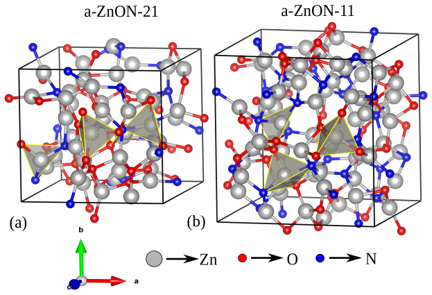
Amorphous structures of zinc oxy-nitrides (Znx+1.5yOxNy) were generated for two stoichiometries of x:y (O:N) ratios of 2:1 (Zn42O24N12) and 1:1 (Zn60O24N24), hereafter referred to as a-ZnON-21 and a-ZnON-11, respectively. We used an evolutionary algorithm based code USPEX (Universal Structure Predictor: Evolutionary Xtallography)Glass, Oganov, and Hansen (2006); Oganov, Lyakhov, and Valle (2011); Lyakhov et al. (2013) to generate the amorphous structures following the methodology proposed by Nahas et al.Nahas, Gaur, and Bhowmick (2016). A large number of structures, obtained from USPEX for each composition, were sorted according to their energies and the structures having no undesirable bonds and densities 85% of the theoretical density of corresponding crystalline structures were selected for further analysis. Details of the structure generation and sorting are provided in the supplementary information (SI-I) and the representative unit cells for both the compositions of a-ZnON are shown in Fig.1.
We performed a detailed structural analysis of selected structures to calculate average bond lengths (ABL) and average coordination number (ACN). The average bond lengths for Zn-O and Zn-N bonds in both the compositions of a-ZnON were found to be very close to the bond lengths in c-ZnO and c-Zn3N2. The polyhedra shown in Fig.1 suggest that most of the Zn atoms have either 3 or 4 coordination with anions (O/N). The average coordination number (ACN) of Zn with anions was found to be 3.5 for both compositions, which is slightly less than the values of c-ZnO and c-Zn3N2 (both having 4 coordinated Zn atoms with respective anions Hanada (2009); Partin, Williams, and O’Keeffe (1997); Wang (2004)). We attribute this difference to the fact that amorphous structures have densities in the range of 85%-91% of the theoretical density, resulting in more open structures. We also calculated radial distribution function (RDF) and running coordination number (RCN) for the selected amorphous structures and found absence of any long-range order and hence these structures were confirmed to be amorphous in nature. Detailed structural analysis of a-ZnON-21 and a-ZnON-11 structures is provided in the supplementary information (SI-II).
III Electronic structure of a-ZnON and a-IGZO
By nature, amorphous structures lack long range periodicity, making them difficult to be treated using DFT, which works best for periodic structures. However, DFT can still be employed, by making large unit-cells of amorphous materials with random distribution of atomic species. Electronic structure calculations were performed using plane-wave code Quantum Espresso with Perdew-Burke-Ernzerhof (PBE) ultrasoft pseudo-potentials Kohn and Sham (1965); Perdew, Burke, and Ernzerhof (1996); Giannozzi et al. (2009), using a kinetic energy cut-off of 50 Ry, along with a 4x4x4 Monkhorst-Pack k-point grid for the relevant reciprocal space integration.
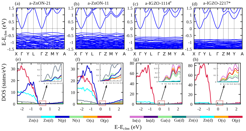
The representative pseudo-band structures (a-d) and the corresponding orbital-resolved partial electronic density of states (PDOS) (e-h), for the two compositions of a-ZnON and a-IGZO, are shown in Fig.2. All amorphous structures were generated in the same way as discussed earlier, except for a-IGZO-2217* (2217 represents the atomic ratios of In, Ga , Zn and O) structure, which was obtained from the previous work of Divya et al. Divya, Prasad, and Deepak (2017). a-IGZO-1114 (1114 represents the atomic ratio of In, Ga, Zn and O) structures were taken from our previous workNahas, Gaur, and Bhowmick (2016) and all the structures have densities in the range of 85%-91% of the theoretical densities of their crystalline counterparts. An apparent band gap at the gamma point shows the semiconducting nature of these amorphous structures. An important difference between the PDOS of a-IGZO and a-ZnON is that the valence band edge of former is made of oxygen-2p orbitals (red), while the valence band edge of latter is made of nitrogen-2p orbitals (blue), which is also consistent with observations reported in literatureNoh et al. (2011); Cho et al. (2009); Nomura et al. (2007b); de Jamblinne de Meux et al. (2015); Park et al. (2016); Kim et al. (2013); Lee et al. (2016). The conduction band edge of a-ZnON is primarily made of Zn-4s orbitals, while in a-IGZO, the conduction band edge is dominated by In-5s orbitals but significant contributions from other metal s-orbitals can also be seen from the insets in PDOS plots of a-IGZO.
While most of the recent literature on a-IGZO attribute overlapping In-5s orbitals as the electron conduction path through the structureNoh et al. (2011); Cho et al. (2009); Nomura et al. (2007b); de Jamblinne de Meux et al. (2015), one of the earliest articles reported overlapping Zn-4s orbitals as the conduction path in a-IGZOOrita et al. (2001).
| a-ZnON-21 | a-ZnON-11 | a-IGZO-1114 | a-IGZO-2217 | ||||
|---|---|---|---|---|---|---|---|
| Orbital | PDOS % | Orbital | PDOS % | Orbital | PDOS % | Orbital | PDOS % |
| Zn-s | 55.53 | Zn-s | 49.90 | In-s | 29.10 | In-s | 35.76 |
| N-s | 14.79 | N-s | 21.09 | O-s | 22.78 | O-s | 22.23 |
| O-s | 13.01 | O-s | 7.24 | Zn-s | 20.11 | Ga-s | 16.29 |
| O-p | 3.59 | N-p | 4.62 | Ga-s | 14.92 | Zn-s | 11.71 |
| N-p | 2.55 | O-p | 2.31 | O-p | 9.50 | O-p | 11.02 |
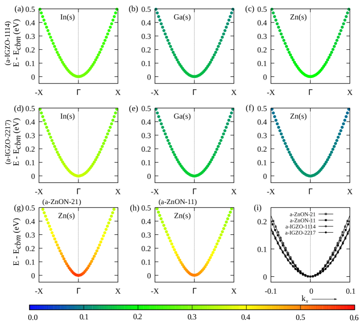
In our calculations for a-IGZO, we see significant contributions form Zn-4s and Ga-4s orbitals to the CBM in PDOS plots (Fig.2 g-h). To quantify the contributions of various metal s-orbitals, we calculated the percentage contribution based on the projection of wavefunctions on atomic basis formed as a linear combination of atomic orbitals, using the method implemented in QE codeSanchez-Portal, Artacho, and Soler (1995). The spilling parameter, which is indicative of mismatch between plane-wave wavefunctions and its projection onto the atomic basis, was found to be very small (0.0019 - 0.0026) for all compositions. In Fig.3, we plot orbital resolved (metal-s orbitals only) band structures in the vicinity of CBM and in Table.1, percentage contributions of metal-s orbitals towards total density of states at the CBM are listed. From Table.1, we see that the contribution of Zn-s orbitals is about 50% at the CBM for a-ZnON structures. For a-IGZO, contributions from different metal-s orbitals are comparable and the contributions from Zn-s and Ga-s orbitals (in comparison to In-s orbitals) cannot be ignored. The contributions towards CBM from different metal-s orbitals also follow chemical composition, as evident from the higher Zn-s contribution in a-IGZO-1114 in comparison to a-IGZO-2217. From the orbital-resolved band structure plot in Fig.3 also, we can see that the contributions of different metal-s orbitals, in the vicinity of CBM, are comparable for a-IGZO compositions. Hence, we argue that the electronic transport in a-IGZO should be through overlapping s-orbitals of different metal cations rather than only In-5s orbitals, as cited in several papers Noh et al. (2011); Cho et al. (2009); Nomura et al. (2007b); de Jamblinne de Meux et al. (2015). For a-ZnON compositions, the highest contribution towards CBM from Zn-4s orbitals is also clearly evident here. A comparison of the curvature at CBM for a-IGZO and a-ZnON compositions (thus comparing the effective mass of the two qualitatively) is shown in Fig.3(i). From this composite conduction band plot, the higher curvature at CBM for a-ZnON is apparent, signifying its lower electron effective mass, which can be related to the higher electron mobilities observed for a-ZnON semiconductors.
In a-IGZO, electron mobility also depends on the carrier concentration (due to the percolation mechanism of electron transportKamiya and Hosono (2010); Hosono (2006)) and increasing In content in the structure increases electron concentration (due to increase in oxygen-vacancies), which explains the observed higher mobility. While increasing Ga content, electron carrier concentration decreases and hence the measured mobilities are comparatively low Kamiya, Nomura, and Hosono (2009); Kamiya and Hosono (2010); Hosono (2006). It is very difficult to deconvolute the role of cations in electron transport from the measured electron mobilities, without including the effect of carrier concentration due to oxygen vacancies. Though, the formation of oxygen vacancies in ionic oxide semiconductors is mainly governed by the thermodynamics of material system, it also heavily depends on the processing conditions, such as partial pressure of oxygen during thin film deposition (sputtering) and/or subsequent annealing. In the next section, we discuss electron transport, at atomic scale, between empty outer s-orbital of two adjacent metal cations in terms of orbital overlap integral to understand the role of metal cations in forming the electron conduction path through these amorphous semiconductors.
IV Orbital overlap integral and electronic conduction
In the previous discussion, we argued that the electronic conduction path must be through overlapping s-orbitals of different cations in a-IGZO and overlapping Zn-4s orbitals in a-ZnON. Therefore, the ease of electron transport (electron mobility) must depend on the nature and extent of overlap between these orbitals. In the following discussion, we attempt to quantify the overlap between outermost s-orbitals of different metal cations in these amorphous semiconductors and relate the overlap to physically verifiable quantities such as electron mobilities. Orbital overlap integral (OI) between different orbitals is a measure of overlap between single electron wavefunctions in these orbitals. Orita et al. Orita et al. (2001) argued that for electron transport in oxide semiconductors, the orbital overlap integral (OI) for metal-s orbitals should be greater than 0.4 and the fraction of metal cations forming the conduction path should be above a percolation threshold of 20%. From the second condition, it is perceptible that in a-IGZO compositions (1114 and 2217), the electron conduction path can not be formed by only a single type of metal cation and hence, in a-IGZO, the conduction path must be through overlapping s-orbitals of different metal cations, while in a-ZnON, the conduction path is through overlapping Zn-4s orbitals. To understand the contribution of different metal-s orbitals and their overlap, we calculated overlap integrals between outermost s orbitals of different pairs of metal ions, for both compositions of a-IGZO and a-ZnON. We followed Mulliken’s formulation for calculating overlap integrals for Slater-type atomic orbitals (STOs) Mulliken et al. (1949). The formulation used in our calculations is given in supplementary information (SI-III). The numerical integrations were carried out using MATHEMATICA Inc. . Different structures for the two compositions of a-IGZO and two compositions of a-ZnON were analyzed to calculate pairwise orbital overlap integrals. A cut-off distance of 4 Å was chosen to be the radius of the interaction sphere around each metal cation and all other cations in the interaction sphere were assumed to have overlapping s orbital with the metal cation in the center. Table.2 shows the number of metal ion pairs, their average distances R (Å) and the orbital overlap integral (OI) for outermost s orbitals, calculated at average distances, for the two compositions of a-IGZO and a-ZnON. The total contribution from a particular metal ion pair per unit volume (Number of Pairs * OI / volume) is also shown in Table.2, which can be compared between different compositions and the sum over all pairs is considered for a-IGZO. We notice a marked difference in the calculated overlap integrals for pairs of similar cations (Zn-Zn, In-In and Ga-Ga) with similar average cation-cation distances, compared to the values reported by Orita et al. Orita et al. (2001) and the orbital overlap between any pair is also less than 0.4, which was proposed as a criteria for forming electron transport path. We ascribe this deviation to the slight difference in way the orbital overlap integrals are calculated. The orbital overlap integral values for different metal-cation pairs range from 0.13 to 0.30, as shown in Table.2. All these cation-pairs should form the conducting pathways for electron transport, however, with varying ease of electron transport between two overlapping orbitals, with higher overlap integral providing less resistance to electron transport.
| (a) | ||||||||
|---|---|---|---|---|---|---|---|---|
| a-IGZO-1114 | a-IGZO-2217 | |||||||
| Voume=1148.19645 Å3 | Voume=1152.70734 Å3 | |||||||
| Pair | No. of Pairs | R (Å) | Overlap Integral | OI*Pairs/Volume | No. of Pairs | R (Å) | Overlap Integral | OI*Pairs/Volume |
| Zn-Zn | 16 | 3.44 | 0.256 | 0.00357 | 3 | 3.48 | 0.248 | 0.00064 |
| In-In | 15 | 3.60 | 0.186 | 0.00243 | 25 | 3.52 | 0.200 | 0.00434 |
| Ga-Ga | 14 | 3.43 | 0.134 | 0.00163 | 22 | 3.31 | 0.154 | 0.00294 |
| In-Zn | 39 | 3.48 | 0.226 | 0.00768 | 32 | 3.51 | 0.222 | 0.00615 |
| In-Ga | 45 | 3.43 | 0.174 | 0.00681 | 56 | 3.53 | 0.157 | 0.00761 |
| Zn-Ga | 39 | 3.28 | 0.222 | 0.00756 | 28 | 3.36 | 0.206 | 0.00500 |
| Sum | 0.02966 | 0.02669 | ||||||
| (b) | ||||||||
|---|---|---|---|---|---|---|---|---|
| a-ZnON-21 | a-ZnON-11 | |||||||
| Volume=1081.7498 Å3 | Volume=1506.9619 Å3 | |||||||
| Pair | No. of Pairs | R (Å) | Overlap Integral | Pairs*OI/Volume | No. of Pairs | R (Å) | Overlap Integral | Pairs*OI/Volume |
| Zn-Zn | 232 | 3.27 | 0.291 | 0.06231 | 337 | 3.23 | 0.299 | 0.06693 |
The sum of all pairwise orbital overlap integrals, normalized to volume (total normalized orbital overlap integral), gives us a parameter to compare electron transport among different structures and compositions. It should be noted that the orbital overlap integral would strongly depend on the density of the amorphous structure, as with increasing density the average distances between metal cation pairs would decrease. For two different compositions of a-IGZO, the total normalized orbital overlap integrals are very similar with slightly higher value for a-IGZO-1114 composition compared to a-IGZO-2217. From Table.2(a), it can be seen that the number of pairs for mix cations is much higher in comparison to the number of pairs of similar cations for a-IGZO. The value of overlap integral is found to be the highest for Zn-Zn pairs, but since the number of pairs are limited, this overlap cannot be solely responsible for the electronic conduction in the material. From the table, it is also evident that for a-IGZO-1114 composition, the main contribution to overall electron transport comes from electron transport between In-Zn, Zn-Ga and In-Ga cation pairs, and for a-IGZO-2217 composition, the main contribution is from electron transport between In-Ga and In-Zn metal-cation pairs. These results are also consistent with our observation of the contribution of different metal s-orbitals in conduction band of a-IGZO (Fig.3 and Table.1). For single cation amorphous structures, such as a-ZnON, electron transport path is always through overlapping s-orbitals of Zn-Zn metal-cation pairs. Since there is only one type of metal-cations present in this system and the average distance between Zn-Zn ions is smaller than pairs of any two cations in a-IGZO, the orbital overlap is higher for a-ZnON in comparison to a-IGZO. Also, owing to the large number of such pairs with higher orbital overlap, the total normalized orbital overlap integral for a-ZnON is much higher (more than a factor of 2) compared to a-IGZO and hence, we may expect the electron transport to be much easier in a-ZnON. From literature Ye, Lim, and White (2009); Yamazaki et al. (2016); Nomura et al. (2004); Kamiya, Nomura, and Hosono (2009); Nomura et al. (2007a); Takagi et al. (2005); Yamaguchi et al. (2009), we know that the measured Hall mobilities for a-ZnON are much higher compared to a-IGZO, which is consistent with higher values of normalized orbital overlap integrals, observed from our calculations, for a-ZnON compared to a-IGZO.
Although we cannot directly relate the total overlap integral with measured values of hall mobilities, there is an apparent correlation between the two. Carrier mobilities in any material depend on the effective mass and the scattering time constants. The scattering mechanisms in amorphous semiconductors are not clearly understood and often difficult to measure or calculate. The carrier effective mass, on the other hand, can be estimated from the electronic structure of material and can give us valuable insight regarding carrier transport. From the pseudo band structures of a-IGZO and a-ZnON in Fig.2, the bottom of the conduction band appears to be symmetric around point and effective mass is calculated by fitting a parabola in small k-range of 0.1 Å-1 in -X direction at the minima and taking the inverse of the curvature (). Since the structures are amorphous, the effective masses in three different directions might be slightly different, owing to different arrangements of ions in the three directions in real space.
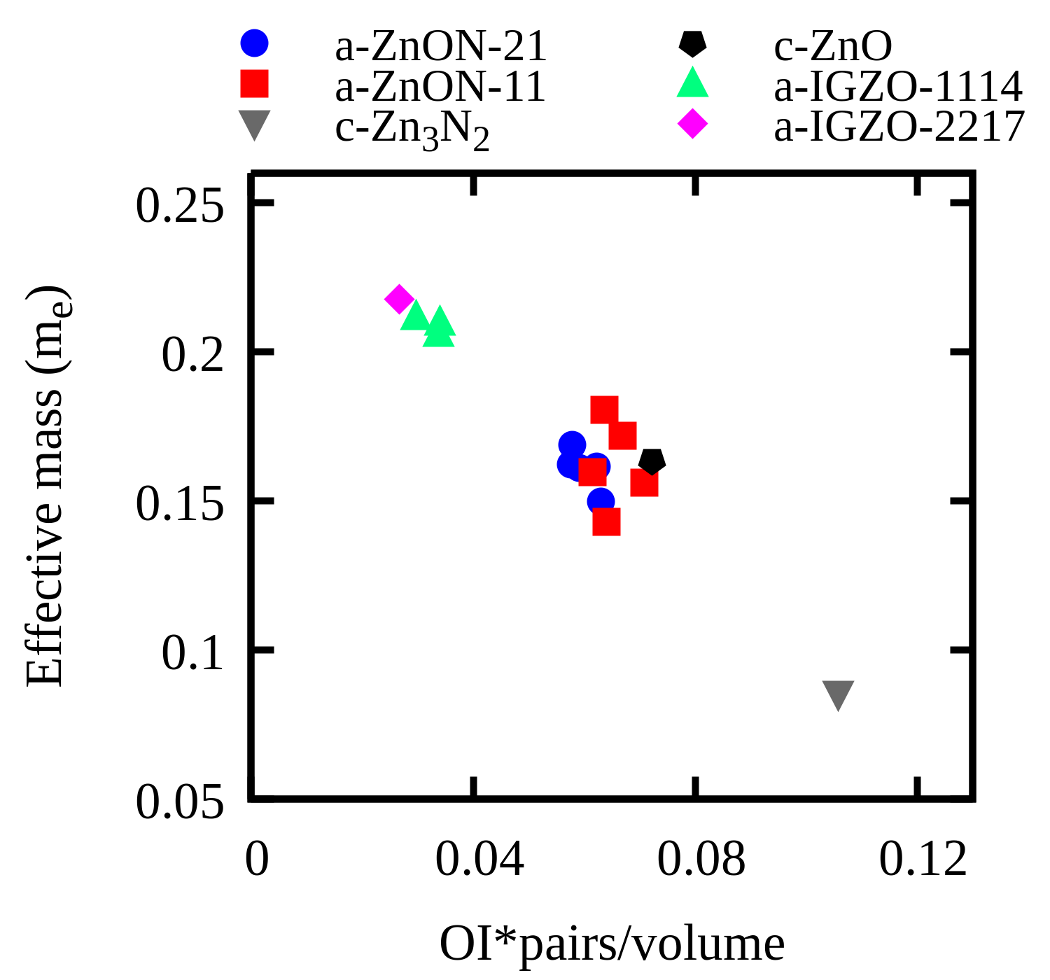
We took the average by calculating the effective masses in all three (-X, -Y and -Z) directions. As shown in Table.2, for a-IGZO-1114 and a-IGZO-2217 structures, the electron effective mass was estimated to be 0.21 me and 0.22 me respectively. While these two values are nearly same, they are small compared to the measured values of 0.34 me Takagi et al. (2005) for electron effective mass in a-IGZO but in agreement with calculated values reported in the Ref.Nomura et al. (2007a). For a-ZnON-11 and a-ZnON-21 structures, as shown in Table.2, the estimated electron effective masses are 0.17 me and 0.16 me respectively, which also match closely with previously reported theoretical value of 0.19 me for electron effective mass in a-ZnON Kim et al. (2013). The smaller electron effective mass observed in a-ZnON compared to a-IGZO, suggest faster electron transport in a-ZnON. Our earlier discussion on total normalized orbital overlap integral also had a similar observation and hence we expect to see some correlation between two calculated values; the effective mass and the total normalized orbital overlap integral59 (59). The difference in calculated electron effective mass between a-IGZO and a-ZnON is not enough to explain the differences in observed electron mobilities in these two materials. The difference in total normalized OI explains the observed difference in mobilities to a better extent but still may not be adequate59 (59). To explore this correlation, we plot (Fig.4) the effective mass and the total normalized orbital overlap integral for different structures of a-IGZO-1114 (three structures), a-IGZO-2217* (one structure), a-ZnON-11 (five structures) and a-ZnON-21 (five structures) compositions. For comparison, we also plot the estimated effective mass and calculated orbital overlap integrals for c-ZnO and c-Zn3N2. From the plot, we can see a strong correlation between effective mass, calculated using ab initio method and the total normalized orbital overlap integral which is calculated from the structural information. Hence, we can use the normalized orbital overlap integral as an estimate for the carrier effective mass and the carrier mobility, for comparison between amorphous structures. The measured Hall mobilities strongly depend on deposition parameters and electron concentration and hence, a direct correlation between measured properties (Hall mobility) with calculated values (effective mass or total normalized OI) can only be qualitative, representing a trend to facilitate further exploration rather than being definitive. Among the two calculated properties; the effective mass and total normalized OI; the total normalized OI seems to relate better with measured mobilities.
V Conclusions
A multi-anion approach towards amorphous semiconductors has distinct advantages over multi-cation based amorphous oxide semiconductors. Comparison of electronic structures of the two materials systems (a-ZnON and a-IGZO) highlights the role of cations and anions in the electronic transport. While the electronic conduction in a-IGZO is found to be through overlapping empty s-orbitals of mixed cations and so it also depends on composition (ratio of cations), in a-ZnON, the electronic conduction path is through overlapping Zn-s orbitals and is independent of composition (ratio of anions). The ease of conduction in these amorphous structure can be estimated in terms of extent of overlap between empty s orbitals of metal cations. The total normalized orbital overlap integral is shown to have a direct correlation with calculated carrier effective mass, this correlation can be used as a qualitative estimate for the observed electron mobilities. Effective mass calculations based on ab initio DFT calculation of electronic structure are computationally expensive, on the other hand, the calculation of the total normalized orbital overlap integral as an estimate for carrier effective mass can be done on for many different amorphous structures or structural averages from many amorphous structures can be calculated with very small computational expense. Calculation of the pairwise orbital overlap integrals for different metal cation pairs also provides an insight into the role of individual metal cations in forming the conduction path in multi-cation amorphous structures which is not straightforward from the DFT calculations. While single structure based DFT calculation are limited in their scope, calculations based on many structures or averages of many structures, such as generated by evolutionary algorithm based codes, should give us better insight into the average properties and role of individual cations/anions in these materials and can be used effectively while predicting properties of new compositions of amorphous semiconductors.
Acknowledgements.
Authors would like to acknowledge support from HPC, IIT Kanpur for use of their computing facility in the present work. J. Srivastava acknowledges financial support from MHRD, Govt. of India and A. Gaur acknowledges support from MeitY, Govt. of India under Visvesvaraya YFRF program. Authors also thank Divya et. al. for providing a-IGZO-2217 structure for comparative studies.References
- Momma and Izumi (2011) K. Momma and F. Izumi, “VESTA3 for three-dimensional visualization of crystal, volumetric and morphology data,” Journal of Applied Crystallography 44, 1272–1276 (2011).
- Powell (1983) M. J. Powell, “Charge trapping instabilities in amorphous silicon-silicon nitride thin-film transistors,” Applied Physics Letters 43, 597–599 (1983).
- Libsch and Kanicki (1993) F. R. Libsch and J. Kanicki, “Bias stress induced stretched exponential time dependence of charge injection and trapping in amorphous thin film transistors,” Applied Physics Letters 62, 1286–1288 (1993).
- Street (2009) R. A. Street, “Thin-Film Transistors,” Advanced Materials 21, 2007–2022 (2009).
- Street (2005) R. Street, Hydrogenated Amorphous Silicon, Cambridge Solid State Science Series (Cambridge University Press, 2005).
- (6) J. Jang, M. H. Choi, and J. H. Cheon, “77.1: Invited Paper: TFT Technologies for Flexible Displays,” SID Symposium Digest of Technical Papers 41, 1143–1146.
- (7) H. D. Kim, J. K. Jeong, H.-J. Chung, and Y.-G. Mo, “22.1: Invited Paper: Technological Challenges for Large-Size AMOLED Display,” SID Symposium Digest of Technical Papers 39, 291–294.
- Hahn (1951) E. E. Hahn, “Some Electrical Properties of Zinc Oxide Semiconductor,” Journal of Applied Physics 22, 855–863 (1951).
- Janotti and de Walle (2009) A. Janotti and C. G. V. de Walle, “Fundamentals of zinc oxide as a semiconductor,” Reports on Progress in Physics 72, 126501 (2009).
- Navamathavan, Choi, and Park (2009) R. Navamathavan, C. K. Choi, and S.-J. Park, “Electrical properties of ZnO-based bottom-gate thin film transistors fabricated by using radio frequency magnetron sputtering,” Journal of Alloys and Compounds 475, 889 – 892 (2009).
- Lee et al. (2012) M.-H. Lee, C.-C. Shih, J.-S. Chen, W.-M. Huang, F.-Y. Gan, Y.-C. Shih, C. X. Qiu, and I.-S. Shih, “15.4: Excellent Performance of Indium-Oxide-Based Thin-Film Transistors by DC Sputtering,” SID Symposium Digest of Technical Papers 40, 191–193 (2012).
- Jin et al. (2014) J. Jin, Y. Luo, P. Bao, C. Brox-Nilsen, R. Potter, and A. Song, “Tuning the electrical properties of ZnO thin-film transistors by thermal annealing in different gases,” Thin Solid Films 552, 192 – 195 (2014).
- Kim et al. (2014) J. Kim, J. Meng, D. Lee, M. Yu, D. Yoo, D. W. Kang, and J. Jo, “ZnO Thin-Film Transistor Grown by rf Sputtering Using Carbon Dioxide and Substrate Bias Modulation,” Journal of Nanomaterials 2014, 7 (2014).
- Hosono, Yasukawa, and Kawazoe (1996) H. Hosono, M. Yasukawa, and H. Kawazoe, “Novel oxide amorphous semiconductors: transparent conducting amorphous oxides,” Journal of Non-Crystalline Solids 203, 334 – 344 (1996), optical and Electrical Propertias of Glasses.
- Hosono et al. (1996) H. Hosono, N. Kikuchi, N. Ueda, and H. Kawazoe, “Working hypothesis to explore novel wide band gap electrically conducting amorphous oxides and examples,” Journal of Non-Crystalline Solids 198-200, 165 – 169 (1996), proceedings of the Sixteenth International Conference on Amorphous Semiconductors - Science and Technology.
- Nomura et al. (2004) K. Nomura, H. Ohta, A. Takagi, T. Kamiya, M. Hirano, and H. Hosono, “Room-Temperature Fabrication of Transparent Flexible Thin-Film Transistors Using Amorphous Oxide Semiconductors,” Nature 432, 488–92 (2004).
- Kamiya, Nomura, and Hosono (2009) T. Kamiya, K. Nomura, and H. Hosono, “Origins of High Mobility and Low Operation Voltage of Amorphous Oxide TFTs: Electronic Structure, Electron Transport, Defects and Doping,” Journal of Display Technology 5, 273–288 (2009).
- Nomura et al. (2007a) K. Nomura, T. Kamiya, H. Ohta, T. Uruga, M. Hirano, and H. Hosono, “Local coordination structure and electronic structure of the large electron mobility amorphous oxide semiconductor In-Ga-Zn-O: Experiment and ab initio calculations,” Phys. Rev. B 75, 035212 (2007a).
- Takagi et al. (2005) A. Takagi, K. Nomura, H. Ohta, H. Yanagi, T. Kamiya, M. Hirano, and H. Hosono, “Carrier transport and electronic structure in amorphous oxide semiconductor, a-InGaZnO,” Thin Solid Films 486, 38–41 (2005).
- Yamaguchi et al. (2009) N. Yamaguchi, S. Taniguchi, T. Miyajima, and M. Ikeda, “Optical and electrical properties of amorphous InGaZnO,” Journal of Vacuum Science & Technology B: Microelectronics and Nanometer Structures Processing, Measurement, and Phenomena 27, 1746–1748 (2009).
- Jeong et al. (2008) J. K. Jeong, J. H. Jeong, J. H. Choi, J. S. Im, S. H. Kim, H. W. Yang, K. N. Kang, K. S. Kim, T. K. Ahn, H.-J. Chung, M. Kim, B. S. Gu, J.-S. Park, Y.-G. Mo, H. D. Kim, and H. K. Chung, “3.1: Distinguished Paper: 12.1-Inch WXGA AMOLED Display Driven by Indium-Gallium-Zinc Oxide TFTs Array,” SID Symposium Digest of Technical Papers 39, 1–4 (2008).
- Ohara et al. (2009) H. Ohara, T. Sasaki, K. Noda, S. Ito, M. Sasaki, Y. Toyosumi, Y. Endo, S. Yoshitomi, J. Sakata, T. Serikawa, and S. Yamazaki, “21.3: 4.0 In. QVGA AMOLED Display Using In-Ga-Zn-Oxide TFTs with a Novel Passivation Layer,” SID Symposium Digest of Technical Papers 40, 284–287 (2009).
- Lee et al. (2011) S. Lee, A. Nathan, J. Robertson, K. Ghaffarzadeh, M. Pepper, S. Jeon, C. Kim, I.-H. Song, U.-I. Chung, and K. Kim, “Temperature Dependent Carrier Transport in Amorphous Oxide Field Effect Transistors ,” IEEE International Electron Device Meeting (IEDM) Tech. Dig. (2011).
- Jeon et al. (2012) S. Jeon, S.-E. Ahn, I. Song, C. J. Kim, U.-I. Chung, E. Lee, I. Yoo, A. Nathan, S. Lee, K. Ghaffarzadeh, J. Robertson, and K. Kim, “Gated three-terminal device architecture to eliminate persistent photoconductivity in oxide semiconductor photosensor arrays,” Nature Materials 11, 301–305 (2012).
- Münzenrieder et al. (2013) N. Münzenrieder, L. Petti, C. Zysset, T. Kinkeldei, G. A. Salvatore, and G. Tröster, “Flexible Self-Aligned Amorphous InGaZnO Thin-Film Transistors With Submicrometer Channel Length and a Transit Frequency of 135 MHz,” IEEE Transactions on Electron Devices 60, 2815–2820 (2013).
- Fortunato, Barquinha, and Martins (2012) E. Fortunato, P. Barquinha, and R. Martins, “Oxide Semiconductor Thin-Film Transistors: A Review of Recent Advances,” Advanced Materials 24, 2945–2986 (2012).
- Ahn et al. (2012a) S.-e. Ahn, S. Jeon, I. Song, Y. Jeon, Y. Kim, C. Kim, J. Lim, W. Jeong, J. Goh, S. Yeon, C. Lee, J.-h. Kim, J.-h. Lee, J. Song, A. Nathan, S. Lee, and U.-i. Chung, “25.2: Photo-Sensor Thin Film Transistor based on Double Metal-Oxide Layer for In-cell Remote Touch Screen,” SID Symposium Digest of Technical Papers 43, 334–337 (2012a).
- Ahn et al. (2012b) S.-E. Ahn, I. Song, S. Jeon, Y. W. Jeon, Y. Kim, C. Kim, B. Ryu, J.-H. Lee, A. Nathan, S. Lee, G. T. Kim, and U.-I. Chung, “Metal Oxide Thin Film Phototransistor for Remote Touch Interactive Displays,” Advanced Materials 24, 2631–2636 (2012b).
- Ye et al. (2013) Y. Ye, R. Lim, H. You, E. Scheer, A. Gaur, H.-c. Hsu, J. Liu, D. K. Yim, A. Hosokawa, and J. M. White, “4.2: Invited Paper: Development of High Mobility Zinc Oxynitride Thin Film Transistors,” SID Symposium Digest of Technical Papers 44, 14–17 (2013).
- Park et al. (2016) J. Park, Y. Soo Kim, K.-C. Ok, Y. Chang Park, H. Kim, J.-S. Park, and H.-S. Kim, “A study on the electron transport properties of ZnON semiconductors with respect to the relative anion content,” Scientific Reports 6, 24787 (2016).
- Ye, Lim, and White (2009) Y. Ye, R. Lim, and J. M. White, “High mobility amorphous zinc oxynitride semiconductor material for thin film transistors,” Journal of Applied Physics 106, 074512 (2009).
- Kim et al. (2013) H.-S. Kim, S. Ho Jeon, J. Park, T. Sang Kim, K. Seok Son, J.-B. Seon, S.-J. Seo, S.-J. Kim, E. Lee, J. Chung, H. Lee, S. Han, M. Ryu, S. Lee, and K. Kim, “Anion control as a strategy to achieve high-mobility and high-stability oxide thin-film transistors,” Scientific reports 3, 1459 (2013).
- Lee et al. (2015a) E. Lee, T. Kim, A. Benayad, H. Kim, S. Jeon, and G.-S. Park, “Ar plasma treated ZnON transistor for future thin film electronics,” Applied Physics Letters 107, 122105 (2015a).
- Lee et al. (2016) E. Lee, T. Kim, A. Benayad, J. Hur, G.-S. Park, and S. Jeon, “High mobility and high stability glassy metal-oxynitride materials and devices,” Scientific Reports 6, 23940 (2016).
- Lee et al. (2015b) S. Lee, A. Nathan, Y. Ye, Y. Guo, and J. Robertson, “Localized Tail States and Electron Mobility in Amorphous ZnON Thin Film Transistors,” Scientific reports 5, 13467 (2015b).
- Yamazaki et al. (2016) T. Yamazaki, K. Shigematsu, Y. Hirose, S. Nakao, I. Harayama, D. Sekiba, and T. Hasegawa, “Amorphous ZnOxNy thin films with high electron Hall mobility exceeding 200 cm2+V-1s-1,” Applied Physics Letters 109, 262101 (2016).
- Glass, Oganov, and Hansen (2006) C. W. Glass, A. R. Oganov, and N. Hansen, “USPEX-Evolutionary crystal structure prediction", journal = "Computer Physics Communications,” 175, 713 – 720 (2006).
- Oganov, Lyakhov, and Valle (2011) A. R. Oganov, A. O. Lyakhov, and M. Valle, “How Evolutionary Crystal Structure Prediction Works—and Why,” Accounts of Chemical Research 44, 227–237 (2011), pMID: 21361336.
- Lyakhov et al. (2013) A. O. Lyakhov, A. R. Oganov, H. T. Stokes, and Q. Zhu, “New developments in evolutionary structure prediction algorithm USPEX,” Computer Physics Communications 184, 1172 – 1182 (2013).
- Nahas, Gaur, and Bhowmick (2016) S. Nahas, A. Gaur, and S. Bhowmick, “First principles prediction of amorphous phases using evolutionary algorithms,” The Journal of Chemical Physics 145, 014106 (2016).
- Hanada (2009) T. Hanada, “Basic Properties of ZnO, GaN, and Related Materials,” in Oxide and Nitride Semiconductors (Springer, 2009) pp. 1–19.
- Partin, Williams, and O’Keeffe (1997) D. Partin, D. Williams, and M. O’Keeffe, “The crystal structures of Mg3N2 and Zn3N2,” Journal of Solid State Chemistry 132, 56–59 (1997).
- Wang (2004) Z. Wang, “Zinc oxide nanostructures: growth, properties and applications,” J. Phys.: Condens. Matter 16, 829–858 (2004).
- Kohn and Sham (1965) W. Kohn and L. J. Sham, “Self-Consistent Equations Including Exchange and Correlation Effects,” Phys. Rev. 140, A1133–A1138 (1965).
- Perdew, Burke, and Ernzerhof (1996) J. P. Perdew, K. Burke, and M. Ernzerhof, “Generalized Gradient Approximation Made Simple,” Phys. Rev. Lett. 77, 3865–3868 (1996).
- Giannozzi et al. (2009) P. Giannozzi, S. Baroni, N. Bonini, M. Calandra, R. Car, C. Cavazzoni, D. Ceresoli, G. L. Chiarotti, M. Cococcioni, I. Dabo, A. D. Corso, S. de Gironcoli, S. Fabris, G. Fratesi, R. Gebauer, U. Gerstmann, C. Gougoussis, A. Kokalj, M. Lazzeri, L. Martin-Samos, N. Marzari, F. Mauri, R. Mazzarello, S. Paolini, A. Pasquarello, L. Paulatto, C. Sbraccia, S. Scandolo, G. Sclauzero, A. P. Seitsonen, A. Smogunov, P. Umari, and R. M. Wentzcovitch, “QUANTUM ESPRESSO: a modular and open-source software project for quantum simulations of materials,” Journal of Physics: Condensed Matter 21, 395502 (2009).
- Divya, Prasad, and Deepak (2017) Divya, R. Prasad, and Deepak, “Recurring polyhedral motifs in the amorphous indium gallium zinc oxide network,” physica status solidi (a) 214, 1600471 (2017).
- Noh et al. (2011) H.-K. Noh, K. J. Chang, B. Ryu, and W.-J. Lee, “Electronic structure of oxygen-vacancy defects in amorphous In-Ga-Zn-O semiconductors,” Phys. Rev. B 84, 115205 (2011).
- Cho et al. (2009) D.-Y. Cho, J. Song, K. D. Na, C. S. Hwang, J. H. Jeong, J. K. Jeong, and Y.-G. Mo, “Local structure and conduction mechanism in amorphous In–Ga–Zn–O films,” Applied Physics Letters 94, 112112 (2009).
- Nomura et al. (2007b) K. Nomura, T. Kamiya, H. Ohta, T. Uruga, M. Hirano, and H. Hosono, “Local coordination structure and electronic structure of the large electron mobility amorphous oxide semiconductor In-Ga-Zn-O: Experiment and ab initio calculations,” Phys. Rev. B 75, 035212 (2007b).
- de Jamblinne de Meux et al. (2015) A. de Jamblinne de Meux, G. Pourtois, J. Genoe, and P. Heremans, “Comparison of the electronic structure of amorphous versus crystalline indium gallium zinc oxide semiconductor: structure, tail states and strain effects,” Journal of Physics D: Applied Physics 48, 435104 (2015).
- Orita et al. (2001) M. Orita, H. Ohta, M. Hirano, S. Narushima, and H. Hosono, “Amorphous transparent conductive oxide InGaO3(ZnO)m (m 4): a Zn4s conductor,” Philosophical Magazine B 81, 501–515 (2001).
- Sanchez-Portal, Artacho, and Soler (1995) D. Sanchez-Portal, E. Artacho, and J. M. Soler, “Projection of plane-wave calculations into atomic orbitals,” Solid State Communications 95, 685 – 690 (1995).
- Kamiya and Hosono (2010) T. Kamiya and H. Hosono, “Material characteristics and applications of transparent amorphous oxide semiconductors,” Npg Asia Materials 2, 15–22 (2010).
- Hosono (2006) H. Hosono, “Ionic amorphous oxide semiconductors: Material design, carrier transport, and device application,” Journal of Non-Crystalline Solids 352, 851 – 858 (2006), amorphous and Nanocrystalline Semiconductors - Science and Technology.
- Mulliken et al. (1949) R. S. Mulliken, C. A. Rieke, D. Orloff, and H. Orloff, “Formulas and Numerical Tables for Overlap Integrals,” The Journal of Chemical Physics 17, 1248–1267 (1949).
- (57) W. R. Inc., “Mathematica, Version 11.0,” Champaign, IL, 2016.
- (58) The calculated effective mass of a-ZnON is about 25% smaller than effective mass of a-IGZO, while the total orbital overlap integral is 2-3 times higher for a-ZnON compared to a-IGZO. Both of these do not adequately explain upto an order of magnitude higher mobilities observed in a-ZnON compared to a-IGZO. However, the difference in total orbital overlap integral is much closer to observed behavior. We speculate that the orbital overlap integral calculations inherently capture some of the physical aspects (such as carrier scattering) of carrier transport and hence able to explain the observed behavior to a larger extent. On the other hand, effective mass calculations are based on DFT calculations, which is applicable to periodic structures and does not describe the scattering behavior at all and it may miss some of the physical aspects of amorphous structures which are captured in total orbital overlap integrals. This may be a subject of further studies to describe carrier transport in multi-component amorphous semiconductors.