Photon-Induced Suppression of Interlayer Tunneling in Van Der Waals Heterostructures
Abstract
We develop a theory for interlayer tunneling in van der Waals heterostructures driven under a strong electromagnetic field, using graphene/h-BN/graphene as a paradigmatic example. Our theory predicts that strong anti-resonances appear at bias voltage values equal to an integer multiple of the light frequency. These features are found to originate from photon-assisted resonant tunneling transitions between Floquet sidebands of different graphene layers, and are unique to two-band systems due to the interplay of both intraband and interband tunneling transitions. Our results point to the possibility of tunneling localization in van der Waals heterostructures using strong electromagnetic fields.
When light is incident on a tunneling junction, inelastic tunneling transitions can occur via the exchange of photons between electrons and the electromagnetic field. This photon-assisted tunneling (PAT) phenomenon was first predicted in the classic work by Tien and Gordon Tien63 in superconductor-insulator-superconductor tunneling junctions SIS_exp . PAT has since been studied and observed in many systems PAT_Rev1 , including semiconductor quantum dots PAT_QD1 ; PAT_QD2 ; PAT_QD3 , double quantum wells PAT_QW and superlattices PAT_SL ; PAT_SL2 , and optical lattices PAT_OL ; PAT_OL2 . In particular, tunneling dynamics can be suppressed DL_2 ; DL_3 ; DL_4 when the light coupling parameter, given by the ratio of the driving field amplitude and frequency, matches a zero of the Bessel function, a celebrated phenomenon called dynamic localization DL .
Van der Waals heterostructures (vdWHs) Antonova16 are an emerging class of nanoscale materials that hold great promise as a platform for realizing unconventional electronic properties and desirable functionalities. Vertically stacked vdWHs exhibit many distinctive properties not available in conventional semiconductor quantum well systems, including enhanced longitudinal and Hall Coulomb drag Drag , tunable metal-insulator transition MIT and extraordinary photovoltaic response Geim . In addition to in-plane transport, vertical tunneling transport in a field-effect tunneling junction geometry exhibits superior current-voltage characteristics TunExp1 ; TunExp2 ; TunExp3 ; TunExp4 ; TunExp5 .
A strong electromagnetic field can provide a heretofore unexplored degree of freedom for tuning the tunneling dynamics in vdWHs. In this Letter, we theoretically investigate interlayer tunneling in optically driven vertical vdWHs, using graphene/h-BN/graphene as an archetypical system. Using the Keldysh-Floquet Green’s function formalism, we formulate a theory for the non-equilibrium PAT current and elucidate the non-perturbative effects of the driving field on the intraband and interband tunneling transitions. Our theory predicts a new type of tunneling localization effect where photon-enabled resonant tunneling processes induce a dramatic suppression of the interlayer tunneling current as a function of the bias voltage, precisely at integer multiples of the photon energy.
Model — Our tunneling structure consists of two parallel graphene layers, labeled as top () and bottom (), that are separated by a middle insulating monolayer of hexagonal boron nitride (h-BN). The layers are perfectly aligned and stacked in the ABA (Bernal) configuration, and a bias voltage is applied across the top and bottom layers. The low-energy excitations around the and points (labeled by , respectively) in the Brillouin zone of each graphene layer is governed by the 2D massive Dirac model up to an energy cutoff :
| (1) |
where is the Dirac velocity, is the band gap induced by the h-BN layer, is the electron charge, and denote the identity and Pauli matrices in the sublattice-pseudospin (i.e., and sites) space. We construct the Hamiltonian of the trilayer system using a nearest-neighbor hopping approximation, including the coupling between each graphene layer and the h-BN layer and ignoring the negligible direct hopping between the graphene sheets. Due to its large band gap , we can trace out the h-BN layer and obtain an effective double-layer Hamiltonian Comment1 , where . Tilde symbolizes the layer-pseudospin (i.e., and ) space. It is convenient to define , , and use the new basis for the layer pseudospins to write the unperturbed Hamiltonian as and the interlayer tunneling Hamiltonian as . The tunneling matrix elements are given by with , where is the interlayer hopping energy from site in graphene to site in h-BN (or vice versa) and is the h-BN band gap.
We consider the two graphene layers to be coupled, for simplicity, to the same optical field by imagining two independent but identical laser sources setup symmetrically on both sides of the vdWH, illuminating the two graphene layers at normal incidence. Thus, the surface electric fields on both layers will be in phase with the same amplitude and frequency. Choosing the propagation direction along the axis, the incident light with electric field amplitude , frequency , and polarization is described by the vector potential . The Peierls substitution in the original Hamiltonian produces the time-dependent Hamiltonian , with the interaction , where . The ratio with describes the amplitude of the interaction in dimensionless form.
Theory — Our formalism is developed by treating the interlayer tunneling Hamiltonian as a perturbation while taking into account the optical field non-perturbatively. Noting that the total charge is conserved in the system, the interlayer electric current density takes the form , where counts the spin degeneracy, is the normalization area, is the canonical ensemble average, and is the electric current with being the electric charge operator on layer T and B. The time evolution of is determined from the equal-time lesser Green’s function, . In a non-equilibrium steady state (NESS), the system respects time translational symmetry and is thus governed by the Floquet theorem Grifoni98 . By using the Floquet mode expansion of the Green’s function Oka_Review , we obtain the time-averaged interlayer electric current density , where an overhat refers to a quantity in the Floquet space, the subscript “” of the Green’s function refers to its off-diagonal element in the layer subspace, “” is the trace over sublattice pseudospins and Floquet modes, and is the identity matrix in the Floquet space.
The lesser Green’s function can be calculated within the Keldysh-Floquet Green’s function formalism Lee17 ; Lee14 ; Tsuji09 . The full, tunneling-coupled Green’s function is uniquely determined by the uncoupled Green’s function of each layer and the interlayer tunneling Hamiltonian via the Dyson equation in the Keldysh-Floquet space InCond . Expansion of up to first order in yields the following photon-assisted tunneling current formula:
| (2) |
where is the retarded Floquet Green’s function of the T and B layers, is the lesser Floquet Green’s function in the absence of light. Coupling to the metallic leads provides the energy relaxation mechanism and is captured by a band broadening parameter in the Green’s functions InCond . We have defined an effective photon-dressed interlayer tunneling Hamiltonian
| (3) |
where and the overbar denotes a complement, e.g., . Eq. (2) together with Eq. (3) is a central result of this Letter. It shows that non-perturbative photon dressing effects are contained not only in the Floquet Green’s function , but also in the tunneling Hamiltonian through Eq. (3), in which the second term within the brackets represents the modification of the tunneling amplitude by a strong optical field.
To illustrate the physics contained in Eq. (2) and also to connect with the more familiar case without light, let us first consider the weak coupling regime Lee17 ; weak_coupling defined as . In this scenario the photon-induced correction to the tunneling Hamiltonian [Eq. (3)] is negligible. For the ABA stacking configuration of our system, where label the sublattice pseudospins, we can reduce Eq. (2) to a compact form
| (4) | |||
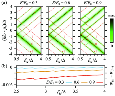
where and is the frequency in the extended zone scheme Oka_Review . The two terms of Eq. (4) correspond to a forward and a backward tunneling channel, and each channel is modified by non-perturbative light coupling effects through the Floquet mode spectral function . In the absence of optical fields, recovers its equilibrium counterpart with Eq. (4) reducing to the well-known 2D-to-2D tunneling current formula 2D_Tunneling1 ; 2D_Tunneling2 . Fig. 1(a) shows the Floquet mode spectral function as a function of the equilibrium energy dispersion for different values of the driving field . At small values of , the quasienergy dispersions of the Floquet sidebands (i.e., photon-dressed electronic bands) approximately coincide with copies of the equilibrium bands shifted by integer multiples of , and the reduced-zone Floquet quasienergy . The undressed conduction and valence bands each generate their own Floquet sidebands, which for convenience will be called Floquet conduction and valence sidebands (FCSB and FVSB, respectively). As increases, mixing between Floquet states becomes stronger and quasienergy band gaps appear prominently at the locations of anti-crossing, given by with .
Single-photon excitations — Before carrying out fully numerical calculations of Eq. (2), we first perform a second-order perturbative analysis in the driving field amplitude. In this work, we focus on low temperatures and evaluate the tunneling current, assuming each graphene layer is at half-filling so that the electrochemical potential under bias is . Treating the light field as a perturbation and expanding the single-layer Green’s function into Comment1 , Eq. (2) can be written in the form , where the zeroth order term J_0_expression yields the dark tunneling current Vasko13 ; Brey ; Polini . The first-order contribution because vanishes under time-averaging. Fig. 2(a) shows, for different values of frequency, the tunneling current obtained within the present second-order perturbation theory. It is seen that the overall profile remains close to the dark tunneling current (dashed line) except at . When the bias voltage is equal to the photon energy, tunneling transitions assisted by a single photon occur, manifesting as a single anti-resonance in the second-order contribution .
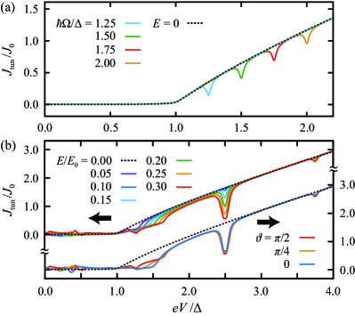
Photon-assisted tunneling suppression — To account for strong field and multiphoton excitation effects, we now evaluate the tunneling current from Eqs. (2)-(3) non-perturbatively. Fig. 2(b) shows our full numerical results for different field strengths (upper set of solid lines) and for different polarization angles (lower set) with an optical frequency value slightly larger than the band gap. In the absence of light, the dark tunneling current remains zero when the bias voltage is smaller than the band gap, as shown by the dashed lines in both Figs. 2(a)-(b). When light is turned on, we first notice that the PAT current becomes non-zero even when , a feature not captured by the second-order perturbation theory. For bias values greater than the band gap , our theory predicts periodic anti-resonance suppression of the tunneling current with a separation along the bias voltage axis as seen in Fig. 2(b). Remarkably, the anti-resonance positions are found to be independent of the field strength and polarization angle , and are precisely given by integer multiples of , i.e., with . Close to the band gap in particular, we find a dramatic suppression of the PAT current to almost zero from its dark value due to the first anti-resonance located at . Fig. 2(b) also shows that the strength of the anti-resonances increases with the field strength, resulting in a progressive suppression of the tunneling current and indicating a tendency towards complete localization at stronger fields. Note here that the nature of our predicted tunneling suppression under optical illumination is fundamentally different from dynamic localization DL ; Grifoni98 ; Kohler , which occurs only when the coupling parameter is equal to a zero of the Bessel function.
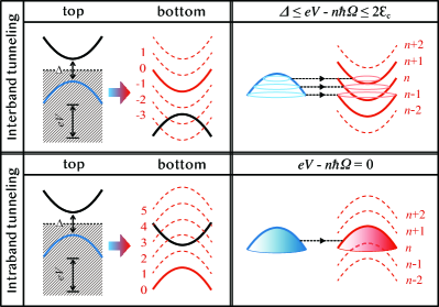
The periodic occurrence of the tunneling suppression uncovered by our calculations stems from resonant intraband tunneling assisted by multiphoton excitations. Let us first consider the case without illumination. Due to conservation of in-plane momentum, conventional 2D-to-2D intraband tunneling in coupled semiconductor quantum wells occurs when the layers’ Fermi levels are closely matched, and resonance tunneling happens at exact matching whereby becomes sharply peaked (here is the electron’s lifetime) Eisenstein . Graphene allows for interband tunneling when the bias voltage exceeds the band gap. If illumination is absent in our system, only interband (but not intraband) tunneling can occur since the layers’ Fermi levels are assumed to be inside the band gap. However, an optical driving field opens up many additional channels for intraband tunneling via photon-assisted transitions between Floquet sidebands (see Fig. 3). When one layer’s undressed valence band (VB) edge is aligned with one of the many FVSB edges of the other layer, electron momentum and energy conservation are simultaneously satisfied and resonant tunneling can occur. This Floquet band edge alignment happens when the bias voltage is tuned to an integer multiple of the driving frequency. To understand why a suppression instead of an enhancement occurs, it is useful to refer to Eq. (4) under a forward bias condition . Physically, the forward tunneling contribution involves tunneling from the undressed VB in the top layer to the FVSBs in the bottom layer (Fig. 3), while the backward tunneling contribution involves tunneling from the undressed VB in the bottom layer to the FVSBs in the top layer. Because they are further removed from the FCSBs, the FVSBs carry a higher spectral weight than their counterparts specfun , as confirmed by our numerical calculations of integrated spectral weights of the Floquet mode spectral function [Fig. 1(b)]. As a result, under the resonant condition , the backward tunneling contribution is dramatically enhanced causing a suppression of .
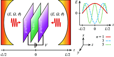
Proposed experimental setup — We close by commenting on the conditions for observability. The assumption that the electromagnetic field on the two graphene layers are the same is not a stringent requirement and using a single light source to illuminate the system does not preclude the resonant tunneling suppression from occurring. Taking account of light reflections, the graphene layer further removed from the light source will experience a driving field with a weaker amplitude but nonetheless the same frequency. The resonant tunneling suppression is therefore expected to occur at the same values of bias voltage albeit with less pronounced anti-resonances. To realize the condition with the same electric field ampitudes on both layers using a single laser, two alternative scenarios can be devised. First, this condition can be approximately achieved when the laser wavelength is long compared with the thickness of the vdWH. Second, an optical cavity can be used (see Fig. 4). When the cavity mode of the standing wave is odd and the vdWH is placed at the cavity’s center, both graphene layers will experience the same magnitude of electromagnetic field.
The resonant intraband tunneling mechanism we discovered is a generalization of the usual dark resonant tunneling to the scenario with Floquet sidebands under strong optical illumination. This phenomenon should apply not only to graphene layers, but also to trilayer vdWHs with other 2D materials such as bilayer graphene and transition-metal dichalcogenides. The fact that the tunneling current can be turned on and off by illumination at frequency values equal to an integral fraction of the bias voltage suggests a time-dependent control scheme for switching applications, opening the door to dynamical tuning of tunneling dynamics using periodic drives.
Acknowledgements.
We thank Patrick Kung, Takashi Oka, and Godfrey Gumbs for useful discussions. This work was supported by startup funds from the University of Alabama and the U.S. Department of Energy, Office of Science, Basic Energy Sciences under Early Career Award DE-SC0019326.References
- (1) P. K. Tien and J. P. Gordon, Multiphoton Process Observed in the Interaction of Microwave Fields with the Tunneling between Superconductor Films, Phys. Rev. 129, 647 (1963).
- (2) A. H. Dayem and R. J. Martin, Quantum Interaction of Microwave Radiation with Tunneling Between Superconductors, Phys. Rev. Lett. 8, 246 (1962).
- (3) G. Platero and R. Aguado, Photon-assisted transport in semiconductor nanostructures, Phys. Rep. 395, 1 (2004).
- (4) L. P. Kouwenhoven, S. Jauhar, K. McCormick, D. Dixon, P. L. McEuen, Yu. V. Nazarov, N. C. van der Vaart, and C. T. Foxon, Photon-assisted tunneling through a quantum dot, Phys. Rev. B 50, 2019(R) (1994).
- (5) L. P. Kouwenhoven, S. Jauhar, J. Orenstein, P. L. McEuen, Y. Nagamune, J. Motohisa, and H. Sakaki, Observation of Photon-Assisted Tunneling through a Quantum Dot, Phys. Rev. Lett. 73, 3443 (1994).
- (6) C. A. Stafford and N. S. Wingreen, Resonant Photon-Assisted Tunneling through a Double Quantum Dot: An Electron Pump from Spatial Rabi Oscillations, Phys. Rev. Lett. 76, 1916 (1996).
- (7) H. Drexler, J. S. Scott, S. J. Allen, K. L. Campman, and A. C. Gossard, Photon-assisted tunneling in a resonant tunneling diode: Stimulated emission and absorption in the THz range, Appl. Phys. Lett. 67, 2816 (1995).
- (8) B. J. Keay, S. J. Allen Jr., J. Galán, J. P. Kaminski, K. L. Campman, A. C. Gossard, U. Bhattacharya, and M. J. W. Rodwell, Photon-Assisted Electric Field Domains and Multiphoton-Assisted Tunneling in Semiconductor Superlattices, Phys. Rev. Lett. 75, 4098 (1995).
- (9) G. S. Vieira, S. J. Allen, P. S. S. Guimarāes, K. L. Campman, and A. C. Gossard, Resonantly enhanced photon-assisted tunneling in a multiple-quantum-well superlattice, Phys. Rev. B 58, 7136 (1998).
- (10) C. Sias, H. Lignier, Y. P. Singh, A. Zenesini, D. Ciampini, O. Morsch, and E. Arimondo, Observation of Photon-Assisted Tunneling in Optical Lattices, Phys. Rev. Lett. 100, 040404 (2008).
- (11) R. Ma, M. E. Tai, P. M. Preiss, W. S. Bakr, J. Simon, and M. Greiner, Photon-Assisted Tunneling in a Biased Strongly Correlated Bose Gas, Phys. Rev. Lett. 107, 095301 (2011).
- (12) B. J. Keay, S. Zeuner, S. J. Allen Jr, K. D. Maranowski, A. C. Gossard, U. Bhattacharya, and M. J. W. Rodwell, Dynamic localization, absolute negative conductance, and stimulated, multiphoton emission in sequential resonant tunneling semiconductor superlattices, Phys. Rev. Lett. 75, 4102 (1995).
- (13) K. W. Madison, M. C. Fischer, R. B. Diener, Qian Niu, and Mark G. Raizen, Dynamical Bloch band suppression in an optical lattice, Phys. Rev. Lett. 81, 5093 (1998).
- (14) S. Longhi, M. Marangoni, M. Lobino, R. Ramponi, P. Laporta, E. Cianci, and V. Foglietti, Observation of dynamic localization in periodically curved waveguide arrays, Phys. Rev. Lett. 96, 243901 (2006).
- (15) D. H. Dunlap, and V. M. Kenkre, Dynamic localization of a charged particle moving under the influence of an electric field, Phys. Rev. B 34 6, 3625 (1986).
- (16) I. V. Antonova, Vertical Heterostructures Based on Graphene and Other 2D Materials, Semiconductors 50, 66 (2016).
- (17) R. V. Gorbachev, A. K. Geim, M. I. Katsnelson, K. S. Novoselov, T. Tudorovskiy, I. V. Grigorieva, A. H. MacDonald et al., Strong Coulomb drag and broken symmetry in double-layer graphene, Nature Phys. 8, 896 (2012).
- (18) L. A. Ponomarenko, A. K. Geim, A. A. Zhukov, R. Jalil, S. V. Morozov, K. S. Novoselov, I. V. Grigorieva et al., Tunable metal-–insulator transition in double-layer graphene heterostructures, Nature Phys. 7, 958 (2011).
- (19) L. Britnell, R. M. Ribeiro, A. Eckmann, R. Jalil, B. D. Belle, A. Mishchenko, Y.-J. Kim, R. V. Gorbachev, T. Georgiou, S. V. Morozov, A. N. Grigorenko, A. K. Geim, C. Casiraghi, A. H. Castro Neto, K. S. Novoselov, Strong Light-Matter Interactions in Heterostructures of Atomically Thin Films, Science 340, 1311 (2013).
- (20) L. Britnell, R. V. Gorbachev, R. Jalil, B. D. Belle, F. Schedin, M. I. Katsnelson, L. Eaves, S. V. Morozov, A. S. Mayorov, N. M. R. Peres, A. H. Castro Neto, J. Leist, A. K. Geim, L. A. Ponomarenko, and K. S. Novoselov, Electron Tunneling through Ultrathin Boron Nitride Crystalline Barriers, Nano Lett. 12, 1707 (2012).
- (21) L. Britnell, R. V. Gorbachev, R. Jalil, B. D. Belle, F. Schedin, A. Mishchenko, T. Georgiou, M. I. Katsnelson, L. Eaves, S. V. Morozov, N. M. R. Peres, J. Leist, A. K. Geim, K. S. Novoselov, and L. A. Ponomarenko, Field-effect tunneling transistor based on vertical graphene heterostructures, Science 335, 947 (2012).
- (22) L. Britnell, R. V. Gorbachev, A. K. Geim, L. A. Ponomarenko, A. Mishchenko, M. T. Greenaway, T. M. Fromhold, K. S. Novoselov, and L. Eaves, Resonant tunnelling and negative differential conductance in graphene transistors, Nat. Commun. 4, 1794 (2013).
- (23) A. Mishchenko, J. S. Tu, Y. Cao, R. V. Gorbachev, J. R. Wallbank, M. T. Greenaway, V. E. Morozov, S. V. Morozov, M. J. Zhu, S. L. Wong, F. Withers, C. R. Woods, Y.-J. Kim, K. Watanabe, T. Taniguchi, E. E. Vdovin, O. Makarovsky, T. M. Fromhold, V. I. Fal’ko, A. K. Geim, L. Eaves, and K. S. Novoselov, Twist-controlled resonant tunnelling in graphene/boron nitride/graphene heterostructures, Nat. Nanotechnol. 9, 808 (2014).
- (24) T. Georgiou, R. Jalil, B. D. Belle, L. Britnell, R. V. Gorbachev, S. V. Morozov, Y.-J. Kim, A. Gholinia, S. J. Haigh, O. Makarovsky, L. Eaves, L. A. Ponomarenko, A. K. Geim, K. S. Novoselov, and A. Mishchenko, Vertical field-effect transistor based on graphene-WS2 heterostructures for flexible and transparent electronics, Nat. Nanotechnol. 8, 100 (2013).
- (25) See Supplementary Material for detailed derivation.
- (26) M. Grifoni and P. Hänggi, Driven quantum tunneling, Phys. Rep. 304, 229 (1998).
- (27) H. Aoki, N. Tsuji, M. Eckstein, M. Kollar, T. Oka, and P. Werner, Nonequilibrium dynamical mean-field theory and its applications, Rev. Mod. Phys. 86, 779 (2014).
- (28) W.-R. Lee and W.-K. Tse, Dynamical quantum anomalous Hall effect in strong optical fields, Phys. Rev. B 95, 201411(R) (2017).
- (29) W.-R. Lee and K. Park, Dielectric breakdown via emergent nonequilibrium steady states of the electric-field-driven Mott insulator, Phys. Rev. B 89, 205126 (2014).
- (30) N. Tsuji, T. Oka, and H. Aoki, Nonequilibrium Steady State of Photoexcited Correlated Electrons in the Presence of Dissipation, Phys. Rev. Lett. 103, 047403 (2009).
- (31) In our approach, electron thermalization is achieved in two steps: (i) Before switching on the optical field, each graphene layer is tunnel-coupled to a metallic lead on each side to achieve thermal equilibrium resulting in a finite damping rate ; (ii) The optical field is adiabatically switched on with a switch-on time that is long compared with other time scales in the system Adia ; Adia2 . In this condition, the initial NESS can be adiabatically connected to the thermal equilibrium state Lee17 . Readers are referred to the Supplementary Material for a more detailed discussion.
- (32) V. M. Galitsky, S. P. Goreslavsky, and V. F. Elesin, Electric and magnetic properties of a semiconductor in the field of a strong electromagnetic wave, Sov. Phys. JETP 30, 117 (1970).
- (33) S. Schmitt-Rink, D. S. Chemla, and H. Haug, Nonequilibrium theory of the optical Stark effect and spectral hole burning in semiconductors, Phys. Rev. B 37, 941 (1988).
- (34) E. K. Irish, Generalized Rotating-Wave Approximation for Arbitrarily Large Coupling, Phys. Rev. Lett. 99, 173601 (2007).
- (35) L. Zheng and A. H. MacDonald, Tunneling conductance between parallel two-dimensional electron systems, Phys. Rev. B 47, 10619 (1993).
- (36) N. Turner, J. T. Nicholls, E. H. Linfield, K. M. Brown, G. A. C. Jones, and D. A. Ritchie, Tunneling between parallel two-dimensional electron gases, Phys. Rev. B 54, 10614 (1996).
- (37) A closed-form analytic expression can be obtained, see Comment1 .
- (38) F. T. Vasko, Resonant and nondissipative tunneling in independently contacted graphene structures, Phys. Rev. B 87, 075424 (2013).
- (39) L. Brey, Coherent Tunneling and Negative Differential Conductivity in a Graphene/h-BN/Graphene Heterostructure, Phys. Rev. Appl. 2, 014003 (2014).
- (40) K. A. Guerrero-Becerra, A. Tomadin, and M. Polini, Resonant tunneling and the quasiparticle lifetime in graphene/boron nitride/graphene heterostructures, Phys. Rev. B 93, 125417 (2016).
- (41) We have checked that is sufficient for the tunneling current to achieve convergence within the range of bias voltage . Details are provided in Sec. S-3.4 of the Supplementary Material.
- (42) S. Kohler, J. Lehmann, and P. Hänggi, Driven quantum transport on the nanoscale, Phys. Rep. 406, 379 (2005).
- (43) J. P. Eisenstein, New transport phenomena in coupled quantum wells, Superlattices Microstruct. 12, 107 (1992).
- (44) If one imagines the formation of Floquet sidebands in two steps: (1) generation of “Floquet copies” via displacement of the undressed conduction and valence bands each by (where ) and (2) band-mixing between the Floquet copies, then one can readily understand that the FVSBs have a higher spectral weight compared to the FVSBs, because the Floquet copies of the valence band and Floquet copies of the conduction band have less overlap and hence less band-mixing that would result in spectral gaps in the quasienergy dispersions.