Transport Properties in Graphene Superlattices
El Bouâzzaoui Choubabia, Abdellatif Kamala and Ahmed Jellal***a.jellal@ucd.ac.maa,b
aLaboratory of Theoretical Physics, Faculty of Sciences, Chouaïb Doukkali University,
PO Box 20, 24000 El Jadida, Morocco
bSaudi Center for Theoretical Physics, Dhahran, Saudi Arabia
Using Chebyshev polynomials, we study the electronic transport properties of massless Dirac fermions in symmetrical graphene superlattice composed of three regions. Matching wavefunctions and using transfer matrix method, we explicitly determine transmission probability as well as the conductance and Fano factor. At vertical Dirac points, we numerically find that the transmission probability shows transmission gaps, conductance has minimums and Fano factor has maximums.
PACS numbers: 73.63.-b; 73.23.-b; 72.80.Rj
Keywords: Graphene superlattice, transmission, conductance, Fano factor.
1 Introduction
Historically, superlattices started with semiconductor materials and later on have been extended to graphene systems called graphene superlattices. They resulted from graphene submitted to any periodic modulation caused by electrostatic potentials [6, 4, 1, 2, 5, 7, 3], magnetic barriers modulation [11, 8, 9, 10] and others. Experimentally, graphene superlattices may be fabricated by applying a local top gate voltage to graphene [12] or by periodically embedding impurity atoms with scanning tunneling microscopy on graphene surface [13]. Because of their interests, recently graphene superlattices have motivated intense experimental and theoretical investigations [11, 4, 5, 14, 15]. Indeed, many works were devoted to study the electronic band structures of Dirac fermions in graphene superlattices [6, 16, 7, 17, 18]. In graphene superlattices, it has been found that the periodic potential causes additional Dirac points in the band structures and leads to an anisotropy in group velocity of charge carriers causing the collimation of electrons beams[1, 5, 7, 19, 3, 20, 21]. These results allow graphene superlattices to be a candidate for manufacturing the carbon-based nanoelectronic devices.
Shot noise is as a consequence of the quantization of charge and is useful to obtain information on a system, which is not available through conductance measurements. It is characterized by a dimensionless parameter called Fano factor, which is defined as the ratio of noise power to mean current [22]. The null value shows a full correlation and maximal quantum coherence giving rise to a total transmission. When reaches a Poissonian value , the transmission probability is close to zero. It found that for short and wide graphene strips has a maximum value of at Dirac point, which is similar strength to the diffusive metals [23]. Recently, we have showed that new Dirac points appeared in graphene superlattices and their positions depend sensitively on the barrier parameters [24]. Because of such dependence, it is a good task to study the conductance and associated to these new Dirac points.
In our previous work [24], we have studied the electronic band structures of massless Dirac fermions in symmetrical graphene superlattice with cells of three regions. Using the transfer matrix method, we have determined the dispersion relation in terms of different physical parameters. We have numerically analyzed such relation and show that there exist three zones: bound, unbound and forbidden states. In the central zone of the band structures, we have determined and enumerated the vertical Dirac points , opening gaps and additional Dirac points. Finally, we have inspected the potential effect on minibands, the anisotropy of group velocity and the energy bands contours near Dirac points. We have also discussed the evolution of gap edges and cutoff region near the vertical Dirac points.
We extend our work [24] to deal with other issues related to Dirac fermions in symmetrical graphene superlattices with cells of three regions (SSLGSL-3R). Using the transfer matrix method, we show that the transmission amplitude can be written in terms of the second kind Chebyshev polynomials [25]. After getting the current density of incident, reflected and transmitted waves along the -direction, we end up with the transmission probability, conductance and Fano factor. Our numerical results show that at the position of vertical Dirac points the transmission probability has several gaps, conductance has minimums and Fano factor has maximums. These can be controlled externally by tuning on distance of the central region of elementary cell, which is the most interesting parameter of our theory. We report different discussions and comparison with respect to SSLGSL with two regions corresponding to .
The present paper is organized as follows. In section 2, we show how derive the transmission probability using transfer matrix method together with the second kind Chebyshev polynomials for Dirac fermions in SSLGSL-3R. Subsequently, we numerically analyze the transmission probability in terms of the physical parameters of our system with an arbitrary number of cells. In section 3, we use the transmission probability to determine the conductance and Fano factor. These quantities are obtained for a graphene superlattice with a number of elementary cells. Our numerical results are discussed in details to highlight the relationship between the Dirac point locations and the transmission gaps as well as conductance minimums and Fano factor maximums. We conclude our results in the final section.
2 Transmission probability
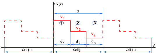
We consider massless Dirac fermions with incident energy from the input region of the symmetrical graphene superlattice with cells of three regions (SSLGSL-3R) at angle , with respect to the -direction as shown in Figure 1. The periodic structure consists of elementary cell labeled by where each one is composed by a juxtaposition of three single square barriers with different height and width , is the width of the entire cell. We apply a potential in elementary cell (Figure 1)
| (1) |
Our graphene superlattice consists of elementary cells, which are interposed between the input and output regions. The massless Dirac fermion in each region of elementary cell is governed by the Hamiltonian
| (2) |
where is the momentum operator, is the Fermi velocity, are the Pauli matrices, is the unit matrix, the index is running from to . The Hamiltonian acts on two components of pseudospinor where are smooth enveloping functions for two triangular sublattices (, ) in graphene and take the forms due to the translation invariance in the -direction. It is convenient to introduce the dimensionless quantities , with and therefore getting the general solution
| (3) |
where both matrices are
| (4) |
with , . The parameters , are the amplitude of positive and negative propagation wavefunctions inside the region , respectively. The wave vector for region takes the form
| (5) |
Using the boundary conditions of wavefunctions at interfaces, we obtain transfer matrix associated with identical unit cells [24]
| (6) |
where reads as
| (7) |
Calculating the determinant and trace of to obtain
| (8) | |||||
where we have introduced the quantity
| (10) |
With (2), we can show that the dispersion relation expression takes the form
| (11) |
To determine the transmission probability it is convenient to write the transfer matrix in terms of Chebyshev polynomials. Then using (35) (see Appendix) to show that (6) can be mapped as
| (12) |
which can be calculated to obtain
| (13) |
We recall that the amplitudes and of the eigenspinors in input and output regions are connected by the following relation
| (14) |
On the other hand, the wave vector of the reflected wave along -direction is opposite to that of the incident wave and the corresponding angle is transformed into [26]. With this we can write the eigenspinors as
| (15) |
where the two components are given by
| (16) |
The current density corresponding to our system can be obtained as
| (17) |
where stands for , and . Using these to derive the incident, reflected and transmitted current density components
| (18) |
giving rise to the transmission and reflection probabilities
| (19) |
because we have (, , ) due to the symmetry of potential configuration in the input and output regions. The solution of (14) provides the transmission coefficient in terms of transfer matrix element
| (20) |
showing that
| (21) |
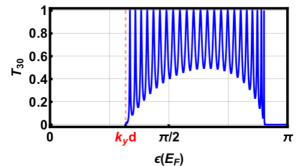
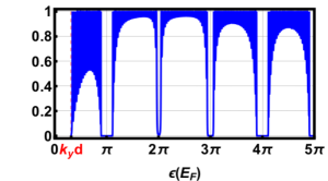
For the numerical analysis, we introduce the rescaled distances () and in order to carry out our computations, we study identical elementary cells of SSLGSL-3R with the conditions , , , . In Figures 2, we present transmission probability as function of incident energy for different values of number of elementary cells . We observe that is clearly affected by number , but its profile converges towards that of superlattice when increases sufficiently up to . When increases, transmission gaps appear at and become deeper, the number of oscillations outside the transmission gaps increases and oscillations reach the total transmission. We notice that similar behavior has been reported in [27].
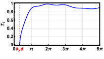
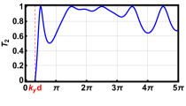
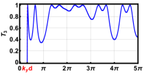
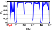
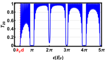
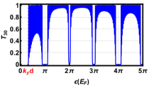
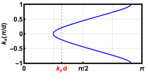
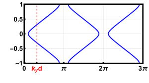
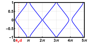
Figure 3 shows the dispersion relation and the corresponding transmission probability versus incident energy for , and three values . In Figures 3LABEL:sub@FigKx:SubFigA, 3LABEL:sub@FigKx:SubFigB, 3LABEL:sub@FigKx:SubFigC we observe that each electronic band presents minibands separated from each other by the band gaps located at energies with different gap widths. Figures 3LABEL:sub@FigTKx:SubFigD, 3LABEL:sub@FigTKx:SubFigE, 3LABEL:sub@FigTKx:SubFigF show that Dirac fermions have zero transmission for energies coinciding with band gaps in electronic band, except for the first near the original Dirac point (ODP) where the transmission is zero up to the value . For the range , we have bound states for all barrier height and therefore the transmission is null. Now for the second range , there is transmission gaps, which are exactly inside of the vertical Dirac points (VDPs) enumerated in our previous work [24]. It is clearly seen that the oscillations of change and become condensated as long as increases.
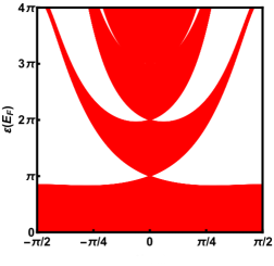
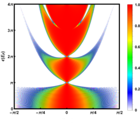
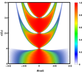
In Figure 4, we present density plots of electronic band structures and transmission probability as function of incident energy and incident angle where , with , and for cases . In Figures 4LABEL:sub@FigBS:SubFigC, 4LABEL:sub@FigBS:SubFigA we observe that there are VDPs located at in the dispersion relation as it was point out in [24]. In Figures 4LABEL:sub@FigTtheta:SubFigD, 4LABEL:sub@FigTtheta:SubFigB we see that when increases the width of each transmission gap increases, where the position of its center is the position of the corresponding VDPs located at with , and the adjacent transmission gaps are separated by . When goes to , with fixed and , the transmission gap is very large. We have a symmetry between positive and negative angles, and then in the forthcoming analysis we will be interested only on the positive ones. In Figure 4, for energies of the band structures lower than that of the first VDP (), one has transmission for all angles and consequently the superlattice behaves like a more refractive medium than that of the pristine graphene. For energies , the reflection is total from a critical angle corresponding to the boundary between the energy band and the first gap where all critical angles in this region take parabolic forms. Beyond the second VDP, other gaps at the level of each VDP with other angles that separate energy bands and gaps, we have angles between two consecutive VDPs and . The change of causes variation of the gap band widths and there is a decrease in the opening of the parabolas when increases, which shows that critical angles can be controlled by tuning on distance .
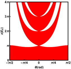
Now let us increase the barrier height to under the same conditions as has been done in Figure 4 with . This gives the density plots presented in Figure 5 where we observe that the locations of the VDPs always remains at the same energy values , the band gaps start as before near the VDPs but their shapes change compared to (Figure 4). Indeed, the parabolic forms of the critical angles disappear by generating energy bands, which cover all the incident angles and the widths of allowed zone became large. In Figures 5LABEL:sub@FigBSVq0:SubFigA and 5LABEL:sub@FigBSVq0:SubFigB, the band gaps are narrow compared to those observed in Figures 5LABEL:sub@FigBSVq13:SubFigC and 5LABEL:sub@FigBSVq13:SubFigD, also we notice that their number decreases. In the range and , a new Dirac point is generated and located between two incident angles and . However such point is eliminated for the case and an opening gap appeared at its place. We see that changing the barrier height the behavior of electronic band structures and transmission changes completely from Figure 4 to Figure 5. This change tells us that we can control both transmission probability by varying such height.
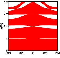
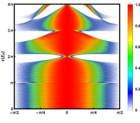
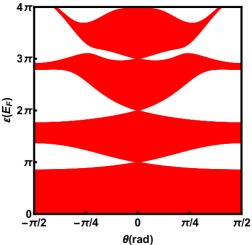
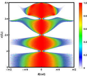
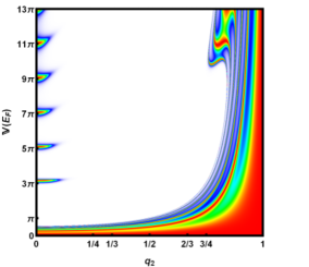
Figure 6 shows density plots of transmission probability as function of potential and distance with , , for three values of incident energy . In the case of pristine graphene which can be realized either by or , we have a total transmission (red color). In the case of SSLGSL-2R (), we have transmission bands intercalated alternately by gaps. By moving away from pristine graphene () increasing either , the energy bands are gradually eliminated and appear in the form of lobes (clusters) surrounded by band gaps, the dimensions of these lobes depend on both and . The band gap is spread over until a band of transmission located on the right hand in Figure 6. This last transmission band has resonance peaks and bumps in its left one for , three for , four for . It is interesting to note that in Figure 6LABEL:sub@FigTq2:SubFigC, the transmission band split into two bands separated by a gap band and when the energy increases the lobes move upwards.
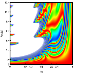
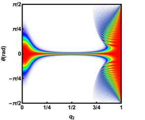
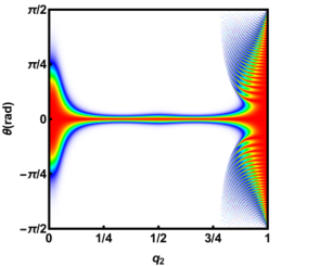
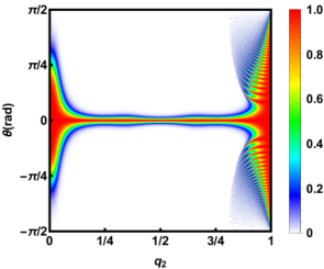
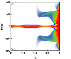
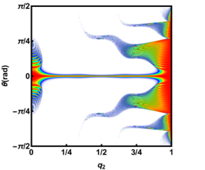
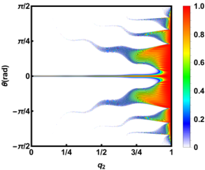
In Figure 7, we present the density plot of transmission probability as function of incident angle and distance with , and for three values of potential . We observe around the normal incident angle for all , there is always a total transmission and when increases a bad gap appears (white color). When is near zero, the transmission band takes place at and becomes large as long as the barrier height increases. Note that, existence of transmission gaps around for three values of is justified by bands intercalated by bad gaps at , see Figure 6LABEL:sub@FigTq2:SubFigA. Now by increasing , one sees that the width of such band along -direction decreases and becomes constant as well as there is apparition of the boosts one for and two for . For , the transmission band takes a form covering all incident angles with resonance peaks.
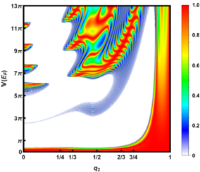
Figure 8 shows the density plot of transmission probability as function of the incident angle and distance with , and for three values of incident energy . We observe that around the normal incident angle for all there is always total transmission. It is clearly seen that for there are lateral bands and when increases these bands tend towards . For odd, when goes to zero, there is a total transmission even for non-null incident angle exhibiting Klein paradox.
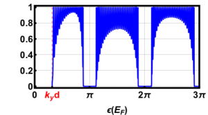
In order to study the effect of the variation of potential on the transmission gaps, we show in Figure 9LABEL:sub@FigTthetaVEq:SubFigA the density plot of transmission probability as function of incident energy and potential . We observe that there are energy regions between the VDPs where the incident electrons can penetrate through the SSLGSL-3R easily, the electrons behave like particles in the free space almost unfettered. The width of transmission gaps located in VDPs increases as long as increases. We see that when is small, the transmission probability is one near VDPs and decreases gradually until transmission gap appeared. In Figure 9LABEL:sub@FigTthetaVEq:SubFigB we present the density plot of transmission probability for SGSL-3R versus incident energy and distance with . We choose and to stay widely near ODP. When varies from to , the system gradually changes from a SSLGSL-2R to a pristine graphene through SSLGSL-3R. The white regions located at , are transmission gaps near VDPs. The white region located near the ODP where , is the transmission gap near this point and has the width of , i.e. when the system becomes pristine graphene. When increases, the width of transmission gaps decreases until its disappearance when the system becomes pristine graphene. When , the band structures contain only the ODP with a purely linear dispersion [24]. This is in perfect match with result presented in our previous work for band structures of SSLGSL-3R [24].
3 Conductance and Fano factor
With the transmission probability , we can obtain the total conductance of the system at zero temperature according to the Landauer Büttiker formula [28]. According to our results, the corresponding ballistic conductance under zero temperature is given by
| (22) | |||||
| (23) |
where is the sample size along the -direction, is the incident angle relative to the direction, and is the conductance unit. Also we consider the Fano factor [23], which can be written as
| (24) |
These results will be investigated numerically to underline our system behavior. In particular, we establish the relationship between two above quantities and the vertical Dirac points (VDPs).
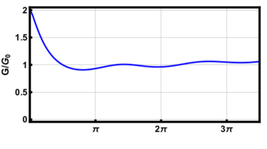
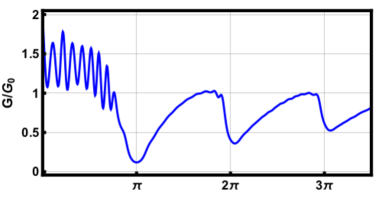
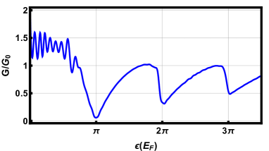
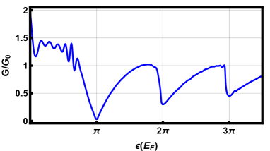
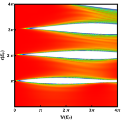
Figure 10 presents the conductance for SSLGSL-3R as function of incident energy with , and different values of elementary cells . We observe that for one cell Figure 10LABEL:sub@FigG:SubFigA, the conductance decreases from value of the pristine graphene to a value just below before the energy is equal to and starts after this value slightly oscillating. When increases the conductance shows minimums located near the levels of VDPs at energies . In Figure 10LABEL:sub@FigG:SubFigB (), the transmission has oscillations between the ODP () and the first VDP (), the first conductance minimum is exactly at the first VDP but the other minimums are close to the relative VDPs. As long as increases (10LABEL:sub@FigG:SubFigC, 10LABEL:sub@FigG:SubFigD), the conductance minimums are placed exactly at the VDPs levels and the oscillations decrease. We find that for , the conductance takes a stable form and therefore we realize it is one corresponding to graphene superlattice. After the first VDP, the conductance varies between and the predict minimums.
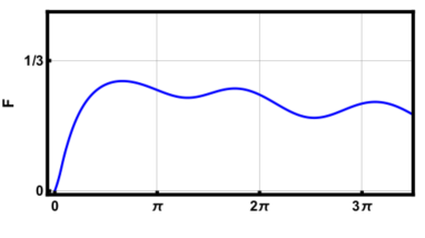
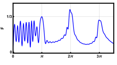
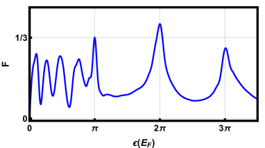
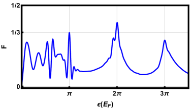
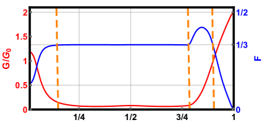
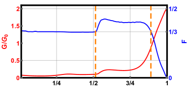
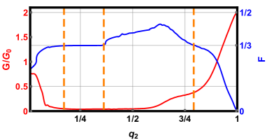
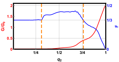
Figure 11 shows the Fano factor versus incident energy with , , for different values . For one cell 11LABEL:sub@FigFN:SubFigA, the Fano factor increases from to value just lower than and starts to decrease again to value higher than . As long as the number increases, more than one maximum of the Fano factor appear at with , as a result of the transmission gaps and conductance. We observe that the Fano factor oscillates intensely at low energy for and as long as increases, the amplitudes and frequencies of oscillation decrease. Note that, for the range of energy the Fano factor does not exceed . However, the Fano factor can exceed (for energy ), which is in agreement with the result found in [27] for SSLGSL-2R.
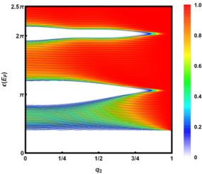
Figure 12 shows the conductance (red line, red frame ticks on left) and Fano factor (blue line, blue frame ticks on right) as function of distance of intermediate region with , and . Let us see what happens in the extreme cases when two critical values of are inspected. Indeed, for meaning that our system behaves as SLGSL-2R, we distinguish two interesting cases. Firstly when (odd values in ) according to Figures 12LABEL:sub@FigGq:SubFigA, 12LABEL:sub@FigGq:SubFigC is always in the interval and is less than . Secondly when (even values in ) Figures 12LABEL:sub@FigGq:SubFigB, 12LABEL:sub@FigGq:SubFigD show that is almost null and is exactly equal . For our system is now a pristine graphene, we observe that for all incident energies and , which are quit normal because in such situation the transmission is total . Still now the cases where is in the range , which means our system is actually a SLGSL-3R. We can divide Figures 12LABEL:sub@FigGq:SubFigA and 12LABEL:sub@FigGq:SubFigC, in four zones according to the range taken by , which are separated by orange dashed vertical lines. We observe that and in first zone, and in second zone, and in third zone, and in forth. However in Figures 12LABEL:sub@FigGq:SubFigB and 12LABEL:sub@FigGq:SubFigD, the first zone is omitted because does not coincide with the transmission bands intercalated alternately by gaps seeing in Figure 6LABEL:sub@FigTq2:SubFigB.
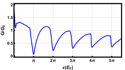
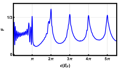
Let us show the conductance and Fano factor for SSLGSL-3R versus incident energy by choosing the case in Figure 13. We clearly observe that the minimum in the conductance at the vertical Dirac points is associated with a maximum in the Fano factor . This result is in agreement with those obtained in literature [29, 23, 26].
4 Conclusion
Using the transfer matrix method and the Chebyshev polynomials of the second kind, we have investigated the transmission probability, ballistic conductance and Fano factor of electrons tunneling through the symmetrical single layer graphene superlattice with three regions (SSLGSL-3R). The corresponding elementary cell is composed of three successive regions of potential (, 0, ), and characterized by three parameters (, , ) where is the elementary cell width and is the width of second region. Explicit calculations showed that the three quantities are functions the physical parameters characterizing our system, which allow us to make derive interesting results and make different discussions.
Interesting numerical results concerning the SSLGSL-3R transmission probability, conductance and Fano factor have been reported. It was shown that the transmission probability density plot has the same behavior of electronic band structure for SSLGSL-3R with . More than one transmission gap exists in the periodic potential structure. More transmission gaps can be obtained by increasing the number of elementary cells. The transmission gaps appear at with , which is the position of VDPs. For energies coinciding with band gaps in electronic band structure, Dirac fermions have zero transmission except for the first near the ODP where the transmission is zero up to the value . The part of the band structure, between zero and , corresponds to the bound states of Dirac fermions where transmission is zero. For potential , in the interval , there is transmission gap, which is exactly on side of the VDPs.
By setting , we show that when increases the width of each transmission gap increases, the position of the center of each transmission gap is the position of the VDPs, and the adjacent transmission gaps are separated by . For the energies of the band structures which are , the superlattice behaves like a more refractive medium than that of the pristine graphene. For the energies , the reflection is total from a critical angle corresponding to the boundary between the energy band and the first gap. Beyond the second VDP, we have emergence of other gaps at the level of each VDP with emergence of other angles that separate energy bands and gaps. We notice that the number of these angles is angles between the and VDPs.
Finally, the conductance and the Fano factor of the periodic potential structure with different values of number of elementary cells are also studied. It was shown that the minimums of conductance and maximums in Fano factor are located exactly at the positions of VDPs. At low energy, the conductance and Fano factor oscillate intensively and when the number of elementary cell increases, the amplitudes and frequencies of oscillation decrease. In our case for the conductance takes a stable form attributed to the SSLGSL-3R. The physical parameter is important to improve and control the conductance and the Fano Factor. We end up our study by choosing the in order to determine the conductance and its Fano factor in SSLGSL-3R.
Acknowledgment
The generous support provided by the Saudi Center for Theoretical Physics (SCTP) is highly appreciated by all authors.
5 Appendix
Given that is a matrix, it turns out that one can write its power in an elegant form involving the Chebyshev polynomials. Indeed, can be expressed as
| (25) |
and generally for any integer , we have
| (26) |
where and are two coefficients of expansion. Pushing our iteration to the next order
| (27) |
multiplying (26) by and using (25) to end up with
| (28) |
which yields the three-term recurrence relations for the coefficient . Next, we will establish a mathematical tools to interpret (28).
Let us now recall some interesting tools which concern the Chebyshev polynomials of the first kind [25]
| (29) |
as well as the second kind are defined
| (30) |
Using the above tools to show that coefficients are Chebyshev polynomials. Indeed, first we set the suitable variable from (30)
| (31) |
where is Bloch phase of the periodic system. Second to determine what kind of Chebyshev polynomials, we calculate and , then comparing (26) for and (25) to write
| (32) |
References
- [1] C.-H. Park, L. Yang, Y.-W. Son, M. L. Cohen, and S. G. Louie, Phys. Rev. Lett. 101, 126804 (2008).
- [2] R. P. Tiwari and D. Stroud, Phys. Rev. B 79, 205435 (2009).
- [3] G. M. Maksimova, E. S. Azarova, A. V. Telezhnikov, and V. A. Burdov, Phys. Rev. B 86, 205422 (2012).
- [4] M. Barbier, F. M. Peeters, P. Vasilopoulos, and J. M. Pereira, Phys. Rev. B 77, 115446 (2008).
- [5] L.-G. Wang and S.-Y. Zhu, Phys. Rev. B 81, 205444 (2010).
- [6] C. Bai and X. Zhang, Phys. Rev. B 76, 075430 (2007).
- [7] M. Barbier, P. Vasilopoulos, and F. M. Peeters, Phys. Rev. B 81, 075438 (2010).
- [8] M. Ramezani Masir, P. Vasilopoulos, A. Matulis, and F. M. Peeters, Phys. Rev. B 77, 235443 (2008).
- [9] M. Ramezani Masir, P. Vasilopoulos, and F. M. Peeters, Phys. Rev. B 79, 035409 (2009).
- [10] L. Dell’Anna and A. De Martino, Phys. Rev. B 79, 045420 (2009).
- [11] S. Ghosh and M. Sharma, J. Phys.: Condens. Matter 21, 292204 (2009).
- [12] B. Huard, J. A. Sulpizio, N. Stander, K. Todd, B. Yang, D. Goldhaber-Gordon, Phys. Rev. Lett. 98, 236803 (2007)
- [13] J. C. Meyer, C. O. Girit, M. F. Crommie, A. Zettl, Appl. Phys. Lett. 92, 123110 (2008)
- [14] X.-X. Guo, D. Liu, and Y.-X. Li, Appl. Phys. Lett. 98, 242101 (2011).
- [15] M. Esmailpour, A. Esmailpour, R. Asgari, M. Elahi, and M. R. Rahimi Tabar, Solid State Commun. 150, 655 (2010).
- [16] L. Brey and H. A. Fertig, Phys. Rev. Lett. 103, 046809 (2009).
- [17] D. P. Arovas, L. Brey, H. A. Fertig, Eun-Ah Kim, and K Ziegler, New J. Phys. 12, 123020 (2010).
- [18] P. Burset, A. L. Yeyati, L. Brey, and H. A. Fertig, Phys. Rev. B 83, 195434 (2011).
- [19] L.-G. Wang and X. Chen, J. Appl. Phys. 109, 033710 (2011).
- [20] C.-H. Park, Y.-W. Son, L. Yang, M. L. Cohen, and S. G. Louie, Nano Lett. 8, 2920 (2008).
- [21] Y. P. Bliokh, V. Freilikher, S. Savel’ev, and F. Nori, Phys. Rev. B 79, 075123 (2009).
- [22] Y. M. Blanter, M. Büttiker, Phys. Rep. 336, 1 (2000)
- [23] J. Tworzydło, B. Trauzettel, M. Titov, A. Rycerz, and C. W. J. Beenakker, Phys. Rev. Lett. 96, 246802 (2006).
- [24] A. Kamal, E. B. Choubabi, and A. Jellal, Eur. Phys. J. B 91, 91 (2018).
- [25] J. C. Mason and D. C. Handscomb, Chebyshev polynomials (CRC Press, 2002).
- [26] A. Jellal, E. B. Choubabi, H. Bahlouli, and A. Aljaafari, J. Low Temp. Phys. 168, 40 (2012).
- [27] Y. Xu, Y. He, and Y. Yang, Physica B: Condens. Matter 457, 188 (2015).
- [28] M. Büttiker, Y. Imry, R. Landauer, and S. Pinhas, Phys. Rev. B 31, 6207 (1985).
- [29] R. Danneau, F. Wu, M. F. Craciun, S. Russo, M. Y. Tomi, J. Salmilehto, A. F. Morpurgo, and P. J. Hakonen, J. Low Temp. Phys. 153, 374 (2008).