Defect-free SnTe topological crystalline insulator nanowires grown by molecular beam epitaxy on graphene
Abstract
SnTe topological crystalline insulator nanowires have been grown by molecular beam epitaxy on graphene/SiC substrates. The nanowires have cubic rock-salt structure, they grow along [001] crystallographic direction and have four sidewalls consisting of {100} crystal planes known to host metallic surface states with Dirac dispersion. Thorough high resolution transmission electron microscopy investigations show that the nanowires grow on graphene in the van der Walls epitaxy mode induced when the catalyzing Au nanoparticle mixes with Sn delivered from SnTe flux, providing liquid Au-Sn alloy. The nanowires are totally free from structural defects, but their {001} sidewalls are prone to oxidation, which points out on necessity of depositing protective capping in view of exploiting the magneto-electric transport phenomena involving charge carriers occupying topologically protected states.
I Introduction
SnTe belongs to a very well-known family of narrow bandgap IV-VI semiconductors, which have been studied because of their interesting electronic properties (Wei and Zunger, 1997) and applications, e.g. in thermoelectric energy harvesting and as mid-infrared detectors and emitters. (Khokhlov, 2002) Quite recently SnTe and some of its ternary (multinary) alloys with Se and/or Pb were identified as topological crystalline insulators (TCI). (Fu, 2011) Indeed IV-VI TCIs host topologically protected Dirac surface states in the vicinity of the distinct points of the Brillouin zone (in this case projection of the L points on the surface Brillouin zone). These states occur due to the coexistence of specific crystalline symmetries, i.e. {110} mirror-plane of rock-salt crystal structure and electronic band inversion of a corresponding bulk crystal. (Hsieh et al., 2012; Dziawa et al., 2012; Xu et al., 2012) The topological protection has been experimentally verified for two high symmetry surfaces of SnTe, namely {100} and {111}, first for {100} surfaces of bulk crystals, either after cleaving (in high vacuum) or for naturally grown crystal facets (Tanaka et al., 2012, 2013; Dybko et al., 2017) and then for the respective surfaces of thin films grown by molecular beam epitaxy (MBE) (Taskin et al., 2014; Zhang et al., 2014) or other methods such as hot-wall epitaxy and e-beam evaporation. (Polley et al., 2016; Zeljkovic et al., 2015; Walkup et al., 2018) With epitaxially grown crystalline layers it is possible to access the topologically protected states on surfaces which are not easy cleavage planes, only reachable when bulk crystals are used. Moreover in thin layer geometry, at some thickness limit, the wavefunctions of topologically protected carriers (Dirac states) start to overlap (Li and Niu, 2017) leading to new phenomena, e.g. occurrence of two-dimensional topological crystalline insulator and quantum spin Hall insulator in the same material. (Safaei et al., 2015) In this letter we report on an interesting kind of low-dimensional structures fabricated from SnTe TCI material, quasi one dimensional nanowires (NWs) deposited on graphene/SiC(6H). The graphene-TI heterostructures are foreseen to exhibit interesting properties due to combination of high mobility 2D graphene charge carriers and the spin-texture of carriers in a TI material. (Song et al., 2018) To our knowledge the MBE growth of SnTe NWs has not been reported before neither on graphene nor on any other substrate. Several literature reports on SnTe NWs and nanocrystals published already (Li et al., 2013; Safdar et al., 2013, 2014; Shen et al., 2014; Zou et al., 2015) concern the nanostructures obtained via chemical vapor deposition technique which cannot compete with MBE in terms of controlling the NW geometrical parameters (lengths and diameters) and the ability to grow NW heterostructures. (Mata et al., 2013)
II Experimental methods
The NWs have been grown by MBE on graphene/SiC(6H) substrates using gold assisted growth mode. Graphene was deposited on a C-face of SiC(0001) by Chemical Vapor Deposition technique, according to the procedure described in Ref. 24. As the source of gold nanocrystals the 10 nm Au nanoparticles (NP) suspended in H2O (BBI solutions) have been used. After wetting graphene/SiC substrate with Au nanoparticles solution the sample was dried using gaseous nitrogen, mounted on the MBE sample holder and introduced to the load lock of the MBE system. After initial degassing at about 200 ∘C the Au(NP)/graphene/SiC substrate was heated to about 700 ∘C, then the substrate temperature was decreased to 400 ∘C – 440 ∘C and the deposition of SnTe was started using compound SnTe source (Knudsen effusion cell) with beam equivalent pressure of about mbar. The growth has been monitored by reflection high energy electron diffraction (RHEED) system. Nanoscale morphologies of the as-grown samples have been investigated by the scanning electron microscope (Hitachi SU-70) operating at acceleration voltage of 15 kV. Structural properties of NWs and of the SnTe/graphene/SiC interface have been investigated with FEI-Titan 80-300 transmission electron microscope operating at 300 kV, equipped with an image corrector. For TEM investigations NWs are transferred to a holey carbon film suported by a Cu mesh mechanicaly, without using any liquid with dispersed NWs. The Helios Nanolab 600 FIB was used to prepare the transparent for electrons SnTe/graphene/SiC interface cross-section by means of focused ion beam techique and lift-off procedure with Oniprobe nanomanipulator. The electron deposited platinum was used first to protect NWs then the thicker ion deposited layer was supplied. The low loss spectra were aquired in STEM mode using The Quantum 966 Gatan Image Filter with energy resolution of about 0.95 eV. EDS spectroscopy was performed using EDAX system. All the TEM investigations have been done at room temperature.
III Results and discussion
Figure 1 shows scanning electron microscopy (SEM) images of SnTe deposited on graphene/SiC substrate at the substrate temperature of 440 ∘C (sample 1) and 400 ∘C (sample 2).
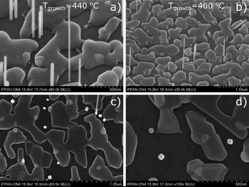
The majority of NWs visible in Fig. 1 are about 0.5 m long and 50 nm thick, occasionally much longer and thinner NWs occur. Apparently, beside the SnTe NWs, the graphene/SiC substrate is also partially covered with planar SnTe. The Au nanocrystals which coagulate and do not catalyze SnTe NWs are visible as brighter spots at the irregular planar SnTe deposits. In spite of slightly lower surface NW densities there are no significant differences in the structure of both samples, but the planar MBE growth of SnTe is slightly more pronounced for sample (2) grown at lower substrate temperature than sample (1).
SEM images taken with e-beam perpendicular to the substrate (parallel to the NWs) – Figs. 1c and 1d indicate that NWs have square cross sections, which corresponds to [001] NW growth axes. We have observed previously that, in contrast to III-V and II-VI semiconductor NWs which usually grow along [111] crystallographic direction, the IV-VI NWs naturally grow along [001] direction, (Dziawa et al., 2010) which implies their 4-fold axial symmetry and square cross section.
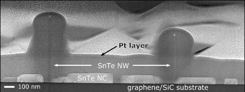
In Figs. 1c and 1d it can be seen that there is lack of correlation of azimuthal orientation of the NWs. However almost all the NWs grow perpendicularly to the substrate. Figure 2 shows focused ion beam (FIB) cross-section acquired from sample (1). Two SnTe NWs embedded in thick platinum layer can be identified in the image.
In the FIB cross-section also the blocks of planar SnTe nanocrystals (NC) are visible. All the NCs have flat surfaces parallel to the interface plane (shown in more details in Fig. 2). The two SnTe NWs indicated on the image are perpendicular to the substrate plane.
Figure 3 shows high resolution HRTEM image of the FIB cross section of SnTe/graphene/SiC hetero-interface (the same specimen measured in different zone axes). The negative spherical aberration imaging (NCSI) mode (Jia et al., 2010) helps in visualizing the carbon atoms in SiC as well as in the graphene interlayer. With the spherical aberration correction settings used ( m) the atomic columns in SiC and graphene appear bright against darker background. Due to the low density of NWs we were unable to find a cross section with SnTe(NW)/substrate interface in the specimen suitable for HRTEM investigations. Only planar SnTe NCs could be identified.
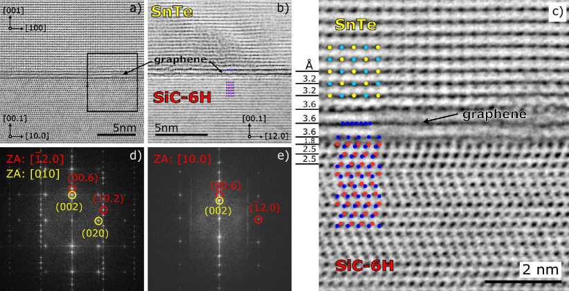
In the interface region with graphene bi-layer we observe the distances between the lattice planes which differ from both SiC and SnTe (see Fig. 3c). Analyzing thoroughly the HRTEM image of this interface we can conclude that SiC is terminated by the carbon layer spaced 1.8 Å from the Si-plane of SiC(6H), similarly to that reported by Norimatsu and Kusunoki. (Norimatsu and Kusunoki, 2009) Next we observe 3.6 Å distance between two graphene planes and the first monolayer of SnTe which is directly placed over the second layer of graphene. The SnTe crystal shown in Fig. 3 is slightly twisted around [001] direction so the atomic structure of SnTe is not perfectly resolved. The visible degradation of graphene interlayer under electron beam was detected after 5 minute exposition to 300 kV electrons and total amorphization appeared after about 20 minutes in the normal HRTEM observation conditions at high magnification.
Even though the cross section shown in Fig. 3 applies to the interface between planar SnTe and graphene/SiC(6H) substrate we believe that the interface between SnTe NW and graphene/SiC(6H) looks the same since similarly to planar SnTe NCs the rock-salt SnTe NWs grow along [001] direction. The planar growth of very thin SnTe (1 to 4 ML) on graphene/SiC substrate has been investigated previously in the context of the robust in-plane SnTe ferroelectric properties. (Chang et al., 2016) The authors of Ref. 28 also observed only (001) orientation of thin SnTe islands deposited by MBE on graphene/SiC. On the other hand for SnTe nanostructures (nanoplates and planar nanowires) deposited on Silicon by CVD technique both (100) and (111) planar SnTe growth have been observed.(Shen et al., 2014)
In spite of the dissimilarities between (001) planes of cubic SnTe, with 4-fold symmetry and the 6-fold symmetry of the graphene/SiC(6H) substrate there is some degree of correlation between SnTe(100) and graphene/SiC(6H), evidenced in the FFT features (see Fig. 3d). In the case of self-catalyzed GaAs NWs grown of graphene (Munshi et al., 2012) such correlation was even more pronounced and concerned also azimuthal correlations between GaAs NWs with [111] growth axes and graphene, which is not observed in our case. For GaAs[111] NWs both the NWs and the substrate share common 6-fold symmetries, which does not occur for (001)SnTe and graphene/SiC(6H).
Figure 4 shows TEM images of a nanowire picked up from sample (2). It can be seen that the surface of the upper NW part (under the catalyst droplet) is smooth as opposed to the bottom where we observe pronounced surface roughness due to oxidation.
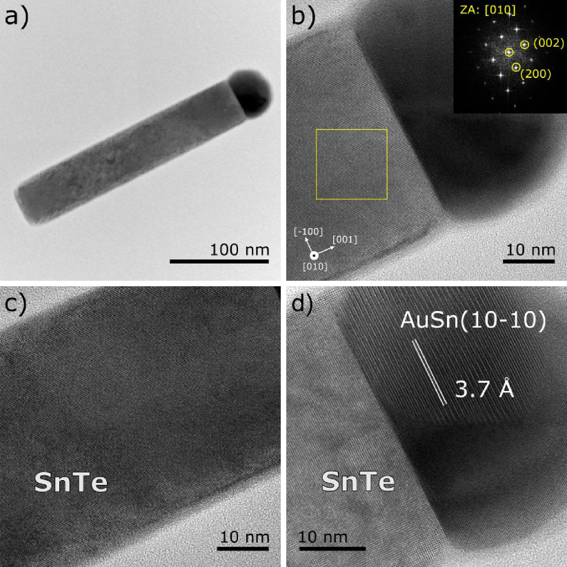
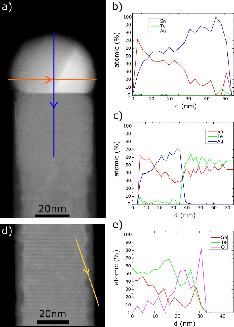
The catalyst nanocrystal at the NW tip shown in Fig. 4d is inhomogeneous; the part visible at the upper section of the image is Sn-rich, as evidenced by the EDS composition scans described further in the text. The spacing between the crystallographic planes clearly visible in the upper part of the solidified droplet corresponds well to 3.74 Å distance between the (10-10) planes of the hexagonal Au0.5Sn0.5 phase. (Arora and Jagirdar, 2014)
As indicated above the SnTe NWs with [001] growth axes are totally free from structural defects. In the NWs shown in Fig. 4 and in many other NWs picked up from samples (1) and (2) the apparent inhomogeneity of the crystalline structure of a solidified catalyst droplet can be seen. The energy dispersion X-ray spectroscopy (EDS) elemental composition scans performed across the droplet (along the orange and blue lines shown in Figs. 5a show that the larger part of the droplet is Sn-rich. The part of the solidified droplet represented with darker contrast in the TEM image is Sn rich, with the Sn content changing from 100% to 20% along the perpendicular scan line and from 60% to 30% along the parallel scan line. The scan directions are indicated by the arrows in Fig. 5a. In this part the atomic planes perpendicular to the NW axes could be identified (see Fig. 4).
Thorough inspection of TEM images of the top part of SnTe NW shown in Fig. 5 reveals that the NW sidewalls are oxidized (see the bottom part of Fig. 5a and Fig. 5d). Amorphous oxide is manifested by slightly darker contrast of the close-to-sidewall region, with respect to that of the NW body. It has been also confirmed by the EDS scan through this region (Fig. 5e). Apparently only the very top part of the NW – down to about 40 nm below the interface with the catalyst droplet is free from oxidation. In some NWs this oxidation is very pronounced, but in all the cases the very top NW parts are protected against oxidation by a thin (2 – 3 ML) film of Au, or Au-Sn alloy (this region is too thin to unequivocally determine its composition). The problem of SnTe oxidation has recently been investigated by Berchenko et al. (Berchenko et al., 2018) The authors of Ref. 31 show that the amorphous oxide at the SnTe(100) surfaces consists of the mixture of Sn and Te oxides and builds up during the first 10 minutes exposure of SnTe to air, then it’s thickness increases slowly in the time-scale of months, and can reach up to 20 nm after 1 – 2 years. In the NWs studied by us we have noticed different degrees of oxidation of NWs picked up from different samples, which have been stored in air for similar time. We cannot directly infer what causes the differences in the oxidation rate; tentatively we attribute that to different stoichiometries of SnTe NWs. An example of NW’s oxidation presented in Fig. 5d and the corresponding EDS profile (Fig. 5e) shows significant contribution of oxygen at the sidewall. The sidewalls of NWs collected from sample (1) grown at 440 ∘C are much more oxidized than those collected from sample (2), grown at 400 ∘C; and due to the known thermodynamic properties of SnTe (Brebrick and Strauss, 1964) we can infer that sample (1) is more Sn-rich than sample (2).
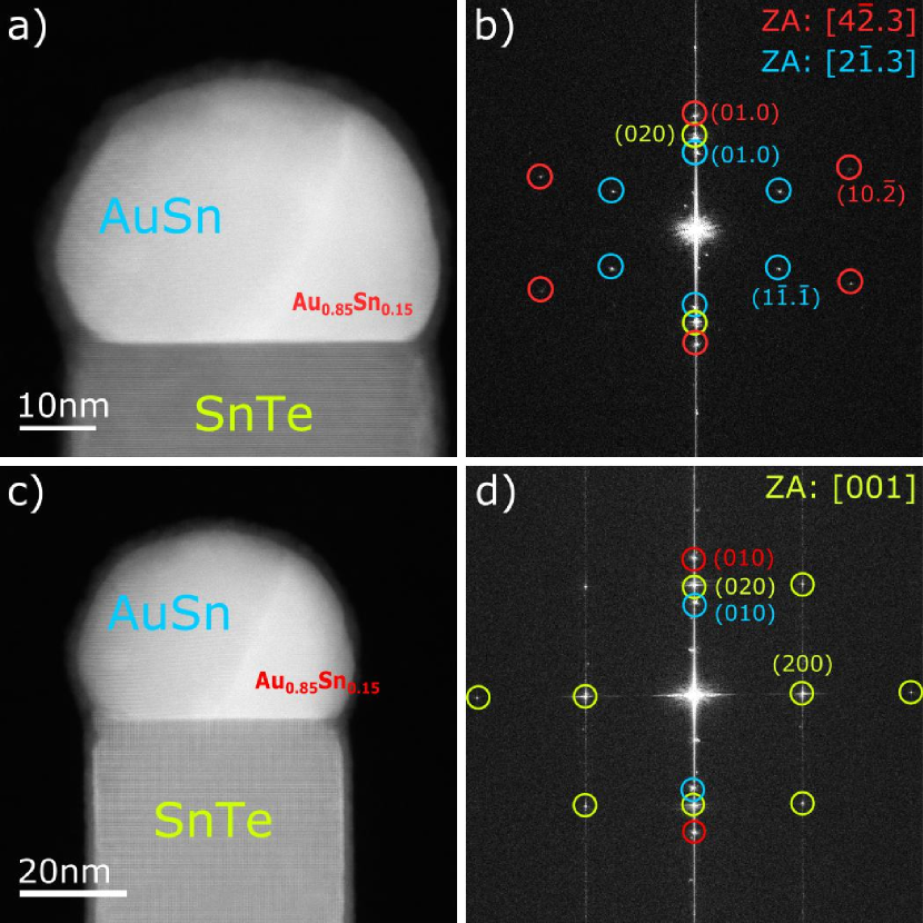
As can be seen in Figs. 5b and 5c the Au rich part of the droplet at the NW tip still contains substantial amount of Sn. To identify which phase of the Au-Sn alloy is present in the droplet we have analyzed the two-dimensional Fast Fourier Transformation (2D FFT) images of the different NW tip and droplet areas (see Fig. 6). The 2D FFT patterns obtained in three different zone axis directions correspond well to: Au0.5Sn0.5 – the main part of the droplet (light blue) and Au0.85Sn0.15 (red). The patterns corresponding to SnTe in the NW body are marked with yellow. Both Au-Sn intermetallic compounds are liquid at the SnTe NWs growth temperature applied here (400 ∘C – 440 ∘C), (Okamoto and Massalski, 1984) which indicates that the metal nanoparticle at the NW tip is in the liquid state during the NWs growth.
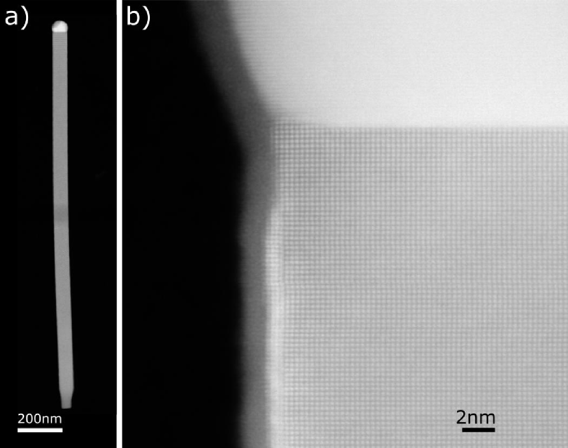
Figure 7 shows two STEM-HAADF images of the SnTe NW grown on graphene/SiC collected from the sample (3) grown at the substrate temperature of 450 ∘C for much longer time (3h) than samples (1) and (2), (1 h). Here the NWs are longer; however they have similar diameters as those picked up from samples (1) and (2) (see Figs. 1, 2 and 4) and are also totally free from structural defects across the whole NW lengths.
Similarly to the NW shown in Figs. 4–6, here the NW axis is also parallel to SnTe[001] crystallographic direction. Likewise, the solidified metal droplet at the NW tip has inhomogeneous composition.
As can clearly be seen in Fig. 7b the outer parts of the NW sidewall edges appear slightly brighter than the NW body (visible in all the SnTe NWs inspected by us). EDS elemental composition scans of this region prove that similarly to the NW shown in Figs. 4–6, in these regions the NW sidewalls are rich in gold and consist of a very thin (2 – 3 ML) film of gold or gold-tin intermetallic alloy. As mentioned before, this very thin Au-rich shell prevents the SnTe NW sidewall from oxidation, which appears as light NW sidewalls necking visible in the lower part of the image shown in Fig. 1a.
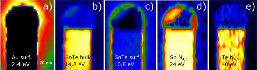
Complementary information about the composition of the top part of SnTe NWs has been obtained by detection of plasmon resonances with use of the electron energy loss spectroscopy (EELS) in STEM. EELS is a powerful technique enabling detections of electron energy losses due to excitation in a broad spectral range from optical energies up to vacuum ultraviolet. (Colliex et al., 2016) Figure 8 shows the 2D maps of EELS intensity obtained by integration of signal for different energy windows spectra of the SnTe NW tip and solidified Au-Sn droplet registered for the NW shown in Fig. 7 (lower energy part of the EELS spectrum), and Sn and Te element distribution mapping due to the signal corresponding to N4,5 edges of both elements. The plasmon-loss spectra are detected for energies corresponding to Au localized surface plasmons (2.4 eV), (Bosman et al., 2007) SnTe volume plasmons (14.8 eV) and SnTe surface plasmons (10.8 eV). (Cook, 1971) The width of the EELS signal integration window was set at 1 eV, 3.4 eV and 3 eV, respectively.
In accordance with EDS and structural information obtained previously, the plasmon resonances observed in EELS confirm the presence of the thin Au-rich film at the top parts of the NW sidewalls. The higher energy part of the EELS spectrum (in the 20 eV – 50 eV range) enables direct elemental mapping of the NW and the metal catalyst at the top. The 2D mapping of the EELS signal corresponding to absorption at Sn N4,5 (24 eV) and Te N4,5 (40 eV) edges (see Figs. 8d and 8e) confirms the inhomogeneous composition of the catalyzing Au-Sn nanoparticle (solid at the TEM measurements temperature), and the negligible amount of Te in it.
IV Conclusions
In summary – we have investigated the Au-assisted MBE growth of SnTe topological crystalline insulator nanowires on graphene/SiC(6H) substrate. The NWs have cubic rock-salt structure and grow along [001] axes which implies their square cross-sections and occurrence of four {100} sidewalls recognized as topologically protected surfaces of the SnTe topological crystalline insulator. Analysis of the metal catalyst nanocrystals at the NW tips reveals that they contain substantial amount of Sn. Two distinct phases of Au-Sn intermetallic alloy: Au0.5Sn0.5 and Au0.85Sn0.15 have been identified in the solidified catalyst droplet. Both phases are liquid at the NW growth temperature (400 ∘C – 440 ∘C) which indicates that the NWs grow in the VLS mode. In the majority of NWs, thoroughly investigated by TEM, no structural defects have been found along the entire NW lengths. In most of the NWs we have observed the oxidation of the NW sidewalls. Only the very top parts of the NWs 40 nm – 80 nm below the catalyzing metal nanoparticle are not oxidized due to protection by the very thin Au-rich film. This points out on necessity of depositing protective shells on the SnTe NW sidewalls in view of studying the transport phenomena involving charge carriers occupying topologically protected states residing at four SnTe(100) NW sidewalls.
Acknowledgements
This work has been supported by the research projects No. 2014/13/B/ST3/04489, and 2014/15/B/ST3/03833 financed by the National Science Centre (Poland). The authors thank the Institute of Electronic Materials Technology and Dr. W. Strupiński for graphene/SiC substrates.
References
- Wei and Zunger (1997) Su-Huai Wei and Alex Zunger, “Electronic and structural anomalies in lead chalcogenides,” Phys. Rev. B 55, 13605–13610 (1997).
- Khokhlov (2002) D. Khokhlov, Lead Chalcogenides: Physics and Applications, Optoelectronic properties of semiconductors and superlattices (Taylor & Francis, 2002).
- Fu (2011) Liang Fu, “Topological crystalline insulators,” Phys. Rev. Lett. 106, 106802 (2011).
- Hsieh et al. (2012) Timothy H. Hsieh, Hsin Lin, Junwei Liu, Wenhui Duan, Arun Bansil, and Liang Fu, “Topological crystalline insulators in the snte material class,” Nature Communications 3, 982 (2012).
- Dziawa et al. (2012) P. Dziawa, B. J. Kowalski, K. Dybko, R. Buczko, A. Szczerbakow, M. Szot, E. Lusakowska, T. Balasubramanian, B. M. Wojek, M. H. Berntsen, O. Tjernberg, and T. Story, “Topological crystalline insulator states in pb1-xsnxse,” Nature Materials 11, 1023 (2012).
- Xu et al. (2012) Su-Yang Xu, Chang Liu, N. Alidoust, M. Neupane, D. Qian, I. Belopolski, J. D. Denlinger, Y. J. Wang, H. Lin, L. A. Wray, G. Landolt, B. Slomski, J. H. Dil, A. Marcinkova, E. Morosan, Q. Gibson, R. Sankar, F. C. Chou, R. J. Cava, A. Bansil, and M. Z. Hasan, “Observation of a topological crystalline insulator phase and topological phase transition in pb1-xsnxte,” Nature Communications 3, 1192 (2012).
- Tanaka et al. (2012) Y. Tanaka, Zhi Ren, T. Sato, K. Nakayama, S. Souma, T. Takahashi, Kouji Segawa, and Yoichi Ando, “Experimental realization of a topological crystalline insulator in snte,” Nature Physics 8, 800 (2012).
- Tanaka et al. (2013) Y. Tanaka, T. Shoman, K. Nakayama, S. Souma, T. Sato, T. Takahashi, M. Novak, Kouji Segawa, and Yoichi Ando, “Two types of dirac-cone surface states on the (111) surface of the topological crystalline insulator snte,” Phys. Rev. B 88, 235126 (2013).
- Dybko et al. (2017) K. Dybko, M. Szot, A. Szczerbakow, M. U. Gutowska, T. Zajarniuk, J. Z. Domagala, A. Szewczyk, T. Story, and W. Zawadzki, “Experimental evidence for topological surface states wrapping around a bulk snte crystal,” Phys. Rev. B 96, 205129 (2017).
- Taskin et al. (2014) A. A. Taskin, Fan Yang, Satoshi Sasaki, Kouji Segawa, and Yoichi Ando, “Topological surface transport in epitaxial snte thin films grown on bi2te3,” Phys. Rev. B 89, 121302 (2014).
- Zhang et al. (2014) Duming Zhang, Hongwoo Baek, Jeonghoon Ha, Tong Zhang, Jonathan Wyrick, Albert V. Davydov, Young Kuk, and Joseph A. Stroscio, “Quasiparticle scattering from topological crystalline insulator snte (001) surface states,” Phys. Rev. B 89, 245445 (2014).
- Polley et al. (2016) C. M. Polley, V. Jovic, T.-Y. Su, M. Saghir, D. Newby, B. J. Kowalski, R. Jakiela, A. Barcz, M. Guziewicz, T. Balasubramanian, G. Balakrishnan, J. Laverock, and K. E. Smith, “Observation of surface states on heavily indium-doped snte(111), a superconducting topological crystalline insulator,” Phys. Rev. B 93, 075132 (2016).
- Zeljkovic et al. (2015) Ilija Zeljkovic, Daniel Walkup, Badih A. Assaf, Kane L. Scipioni, R. Sankar, Fangcheng Chou, and Vidya Madhavan, “Strain engineering dirac surface states in heteroepitaxial topological crystalline insulator thin films,” Nature Nanotechnology 10, 849 (2015).
- Walkup et al. (2018) Daniel Walkup, Badih A. Assaf, Kane L. Scipioni, R. Sankar, Fangcheng Chou, Guoqing Chang, Hsin Lin, Ilija Zeljkovic, and Vidya Madhavan, “Interplay of orbital effects and nanoscale strain in topological crystalline insulators,” Nature Communications 9, 1550 (2018).
- Li and Niu (2017) Xiao Li and Qian Niu, “Topological phase transitions in thin films by tuning multivalley boundary-state couplings,” Phys. Rev. B 95, 241411 (2017).
- Safaei et al. (2015) S Safaei, M Galicka, P Kacman, and R Buczko, “Quantum spin hall effect in iv-vi topological crystalline insulators,” New Journal of Physics 17, 063041 (2015).
- Song et al. (2018) Kenan Song, David Soriano, Aron W. Cummings, Roberto Robles, Pablo Ordejón, and Stephan Roche, “Spin proximity effects in graphene/topological insulator heterostructures,” Nano Letters 18, 2033–2039 (2018).
- Li et al. (2013) Z. Li, S. Shao, N. Li, K. McCall, J. Wang, and S. X. Zhang, “Single crystalline nanostructures of topological crystalline insulator snte with distinct facets and morphologies,” Nano Letters 13, 5443–5448 (2013), https://doi.org/10.1021/nl4030193 .
- Safdar et al. (2013) Muhammad Safdar, Qisheng Wang, Misbah Mirza, Zhenxing Wang, Kai Xu, and Jun He, “Topological surface transport properties of single-crystalline snte nanowire,” Nano Letters 13, 5344–5349 (2013), https://doi.org/10.1021/nl402841x .
- Safdar et al. (2014) Muhammad Safdar, Qisheng Wang, Misbah Mirza, Zhenxing Wang, and Jun He, “Crystal shape engineering of topological crystalline insulator snte microcrystals and nanowires with huge thermal activation energy gap,” Crystal Growth & Design 14, 2502–2509 (2014).
- Shen et al. (2014) Jie Shen, Yeonwoong Jung, Ankit S. Disa, Fred J. Walker, Charles H. Ahn, and Judy J. Cha, “Synthesis of snte nanoplates with {100} and {111} surfaces,” Nano Letters 14, 4183–4188 (2014).
- Zou et al. (2015) Yichao Zou, Zhigang Chen, Jing Lin, Xiaohao Zhou, Wei Lu, John Drennan, and Jin Zou, “Morphological control of snte nanostructures by tuning catalyst composition,” Nano Research 8, 3011–3019 (2015).
- Mata et al. (2013) Maria de la Mata, Xiang Zhou, Florian Furtmayr, Jorg Teubert, Silvija Gradecak, Martin Eickhoff, Anna Fontcuberta i Morral, and Jordi Arbiol, “A review of mbe grown 0d, 1d and 2d quantum structures in a nanowire,” J. Mater. Chem. C 1, 4300–4312 (2013).
- Strupinski et al. (2011) W. Strupinski, K. Grodecki, A. Wysmolek, R. Stepniewski, T. Szkopek, P. E. Gaskell, A. Grüneis, D. Haberer, R. Bozek, J. Krupka, and J. M. Baranowski, “Graphene epitaxy by chemical vapor deposition on sic,” Nano Letters 11, 1786–1791 (2011).
- Dziawa et al. (2010) P. Dziawa, J. Sadowski, P. Dluzewski, E. Lusakowska, V. Domukhovski, B. Taliashvili, T. Wojciechowski, L. T. Baczewski, M. Bukala, M. Galicka, R. Buczko, P. Kacman, and T. Story, “Defect free pbte nanowires grown by molecular beam epitaxy on gaas(111)b substrates,” Crystal Growth & Design 10, 109–113 (2010).
- Jia et al. (2010) C. L. Jia, L. Houben, A. Thust, and J. Barthel, “On the benefit of the negative-spherical-aberration imaging technique for quantitative hrtem,” Ultramicroscopy 110, 500–505 (2010).
- Norimatsu and Kusunoki (2009) Wataru Norimatsu and Michiko Kusunoki, Transitional structures of the interface between graphene and 6H-SiC (0 0 0 1), Chemical Physics Letters - CHEM PHYS LETT, Vol. 468 (2009) pp. 52–56.
- Chang et al. (2016) Kai Chang, Junwei Liu, Haicheng Lin, Na Wang, Kun Zhao, Anmin Zhang, Feng Jin, Yong Zhong, Xiaopeng Hu, Wenhui Duan, Qingming Zhang, Liang Fu, Qi-Kun Xue, Xi Chen, and Shuai-Hua Ji, “Discovery of robust in-plane ferroelectricity in atomic-thick snte,” Science 353, 274 (2016).
- Munshi et al. (2012) A. Mazid Munshi, Dasa L. Dheeraj, Vidar T. Fauske, Dong-Chul Kim, Antonius T. J. van Helvoort, Bjørn-Ove Fimland, and Helge Weman, “Vertically aligned gaas nanowires on graphite and few-layer graphene: Generic model and epitaxial growth,” Nano Letters 12, 4570–4576 (2012).
- Arora and Jagirdar (2014) Neha Arora and Balaji R. Jagirdar, “From (au5sn + ausn) physical mixture to phase pure ausn and au5sn intermetallic nanocrystals with tailored morphology: digestive ripening assisted approach,” Physical Chemistry Chemical Physics 16, 11381–11389 (2014).
- Berchenko et al. (2018) N. Berchenko, R. Vitchev, M. Trzyna, R. Wojnarowska-Nowak, A. Szczerbakow, A. Badyla, J. Cebulski, and T. Story, “Surface oxidation of snte topological crystalline insulator,” Applied Surface Science 452, 134–140 (2018).
- Brebrick and Strauss (1964) R. F. Brebrick and A. J. Strauss, “Partial pressures in equilibrium with group iv tellurides. ii. tin telluride,” The Journal of Chemical Physics 41, 197–205 (1964).
- Okamoto and Massalski (1984) H. Okamoto and T. B. Massalski, “The au-sn (gold-tin) system,” Bulletin of Alloy Phase Diagrams 5, 492 (1984).
- Colliex et al. (2016) Christian Colliex, Mathieu Kociak, and Odile Stéphan, “Electron energy loss spectroscopy imaging of surface plasmons at the nanometer scale,” Ultramicroscopy 162, A1–A24 (2016).
- Bosman et al. (2007) Michel Bosman, Vicki J Keast, Masashi Watanabe, Abbas I Maaroof, and Michael B Cortie, “Mapping surface plasmons at the nanometre scale with an electron beam,” Nanotechnology 18, 165505 (2007).
- Cook (1971) R. F. Cook, “Electron energy loss spectra of gete-snte alloys,” Philosophical Magazine 24, 1347–1353 (1971).