Computer Simulation of Electronic Device for Generation of Electric Oscillations by Negative Differential Conductivity of Supercooled Nanostructured Superconductors in Electric Field
Abstract
We use the formerly derived explicit analytical expressions for the conductivity of nanostructured superconductors supercooled below the critical temperature in electric field. Computer simulations reveal that the negative differential conductivity region of the current-voltage characteristic leads to excitation of electric oscillations. We simulate a circuit with distributed elements as a first step to obtain gigahertz oscillations. This gives a hint that a hybrid device of nanostructured superconductors will work in terahertz frequencies. If the projected setup is successful, we consider the possibility for it to be put in a nanosatellite (such as a CubeSat). A study of high temperature superconductor layers in space vacuum and radiation would be an important technological task. The interface thermal boundary resistance is taken into account in the numerical illustrations for the work of the device.
I Introduction
The purpose of the present work is to present a numerical simulation which shows the generation of high-frequency oscillations created by a thin superconducting film supercooled bellow the critical temperature in external electric field . The idea was first proposed more than 10 years ago TerraHz and now we are giving details on how to start the experimental work using radio frequency oscillations with distributed elements (resistors, capacitors and inductors). The main idea is to insert a supercooled superconductor with negative differential conductivity as an active element in a resonance circuit. The simulation presented in this work aims to trigger the analogous development of terraherz region where the resonance circuit will be implemented on the same hybrid nanodevice which will emit coherent terraherz waves.
II Fluctuation conductivity in electric field
Our starting point is the result for the two-dimensional fluctuational current density in external electric fieldKinetics ; Fluctuation ; Varlamov ; Mishonov
| (1) |
where is the dimensionless electric field and is the reduced temperature
| (2) |
defined by the coherence length
| (3) |
the critical temperature or a time constant , related to the relaxation of the superconducting order parameter
| (4) |
The constant with dimension of conductivity
| (5) |
represents the Aslamazov-Larkin conductivity above for evanescent electric field
| (6) |
The normal conductivity is parameterized by the dimensionless .
The dimensionless function of reduced temperature and electric field
| (7) |
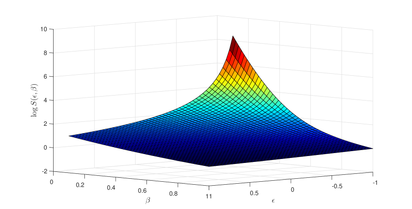
describing the fluctuational conductivity is depicted in Fig. 1. This formula for the current Eq. (7) is a consequence of time-dependent Ginzburg-Landau equation, which is applicable below if the coherent superconducting order parameter is destroyed by constant electric field. For the integral is elementary. In other cases the substitution reduces the integral to well-known special functions.
For low frequencies where the heat capacity of the superconductor is negligible, the temperature of the superconducting layer is determined by the Ohmic heating per unit area and interface boundary resistance
| (8) |
where is a convenient dimensionless parameter useful for the further analysis and is the substrate temperature. Until the critical temperature can be found by fitting the temperature dependence of the resistivity above , the coherence length can be extracted without applying magnetic field from the non-linear fluctuational conductivity Hurault at
| (9) |
Since the fluctuational current formally tends to infinity at evanescent electric field bellow , one can easily derive the asymptotics
| (10) |
which allows us to determine the interface conductance . Or else the current
| (11) |
meaning that we have hyperbolic approximation for the current-voltage characteristic. Here the voltage and the current are given through the strip length and its width . They are related to and through
| (12) |
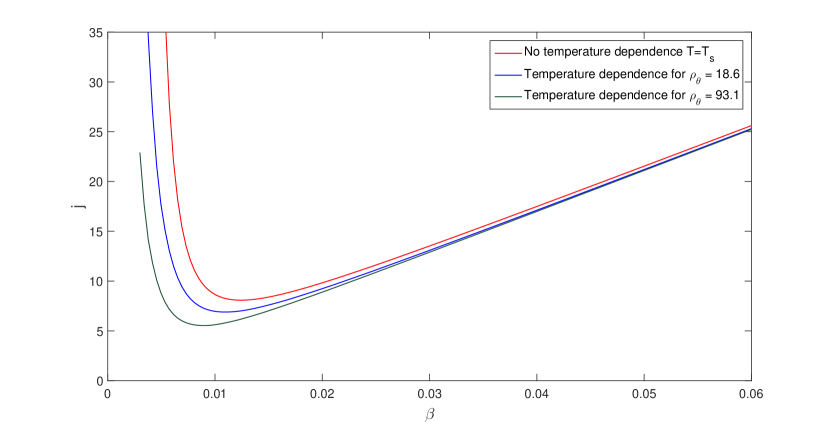
Below the critical temperature at small electric fields the current is significant and the temperature of the superconductor has to be calculated in a self-consistent way solving simultaneously Eq. (8) and Eq. (1) shown in Fig. 2.
The shape of the thin film is not necessarily a strip. For example it can be in Corbino geometry, a narrow ring between radii and with and . Specifically for high superconductors, the frequency is in the terraherz range and for them the above-derived static formulas for the current are valid practically for the whole radio frequency range. In the next section we present a circuit working within the framework of the theory presented so far.
III Circuit generating oscillations
The circuit for generation of stable oscillations by using negative differential conductivity in supercooled superconductors is shown in Fig. 3.
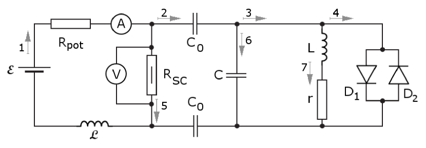
One can easily see the parallel resonance circuit generating the oscillations. In short, the negative differential resistivity amplifies the generated oscillations, while the two oppositely connected diodes and limit the amplitude of the oscillations.
Applying Kirchoff’s laws, the dynamical laws governing the currents and voltages, to the circuit in Fig. 3, the current and voltage equations are easily found to be
| (13) | |||||
| (14) | |||||
| (15) | |||||
| (16) | |||||
| (17) | |||||
| (18) | |||||
| (19) |
This system of equations governs the circuit operation.
The current through the diodes and () is governed by the volt-ampere characteristic
where is the voltage between the two ends of the inductance , is the diode’s conductance when it is ”open” and is its opening voltage. Obviously is entirely determined by the inductance’s voltage, which from Eq. (15) is completely determined by and .
Eliminating , , and and defining the additional functions and
we can rewrite this system as
Defining the matrices , and by
we can write the system as the simple matrix equation
| (20) |
IV Results
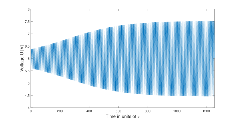
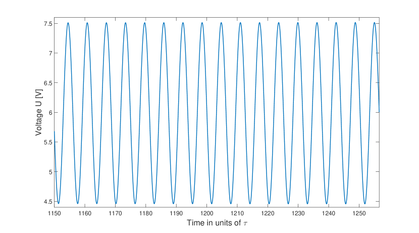
The calculated oscillations generated by the thin supercooled below superconductor from the circuit in Fig. 3 are shown in Fig. 4 and magnified in Fig. 5 with the numerical values presented in Table 1.
| Element | Value | Parameter | Value |
|---|---|---|---|
| 6 V | 20 m | ||
| 10 | 20 m | ||
| 1 mH | 1.5 nm | ||
| 1 mF | 137 | ||
| nF | 80 K | ||
| 100 nH | 90 K | ||
| 0.3 | |||
| 2 V | |||
| 0.1 Sm |
The oscillations are in the GHz region as it is expected from the values of and from Table 1. The diodes are only a schematic element, they can be even omitted since the heating of the superconductor through the interface resistance reliably limits the oscillations. Non-linear effects associated with the boundary resistance in fact limit the oscillations amplitude preventing exponential growth. The average dissipated power is less than 1 Watt. In order to avoid boiling the nitrogen, the use of cryogenic electron microscopy may be required. These results give an optimistic estimate that it is worth starting an experimental research with the available nanostructured samples – a strip of thin film or 2-dimensional superconductor with 2 electrodes at the ends like source-drain channel in a field-effect transistor.
V Conclusions
We demonstrate gigahertz range of electric oscillations created by the negative differential conductivity in external electric field of supercooled below superconductor. Using distributed elements, the frequency of generations is fixed but using as a resonator 2D plasmons, Groshev the resonance frequency can easily reach terahertz range. The theory of damping rate of 2D plasmon will be given elsewhere.
The development work should start with investigation of current voltage characteristics of a nanostructured superconductor similar to a field effect transistor. The area of source and drain should be maximal in order to ensure high currents. If the gate is implemented by de-pairing magnetic material, the described sample will be a new type superconducting field effect transistor operating in the terahertz range. Crucial starting point will be observation of annulation of differential conductivity at decaying electric field below . It was suggested by Gor’kov, Gorkov:70 which tried to interpret the generation of high-frequency electric oscillations in thin superconducting films observed half a century ago. Churilov:69 Now the time has come to develop technical applications based on hybrid nanostructured superconductors. For true 2D superconductors the temperature can be accepted to be equal to the ambient while for thin films it is indispensable to take into account the interface thermal boundary resistance.
Acknowledgements.
Preliminary results from this research were presented in the COST School on Quantum Materials and Workshop on Vortex Behavior in Unconventional Superconductors, 7-12 October 2018 in Braga, Portugal and in the 10th Anniversary International Conference on Nanomaterials – R&A, 17-19 October 2018 in Brno, Czech Republic.NANOCON:18 Authors are thankful to Anna Palau, Andrey Varlamov and Hermann Suderow for the stimulating discussions during the COST school on quantum materials. Authors will greatly appreciate any correspondence related to an experimental realisation of the proposed generator.References
References
- (1) T. M. Mishonov and M. T. Mishonov, “Theory of terahertz electric oscillations by supercooled superconductors”, Supercond. Sci. Technol. 18, 1506–1512 (2005).
- (2) T. M. Mishonov, G. V. Pachov, I. N. Genchev, L. A. Atanasova and D. Ch. Damianov, “Kinetics and Boltzmann kinetic equation for fluctuation Cooper pairs”, Phys. Rev. B 68, 054525 (2003).
- (3) T. M. Mishonov, A. Posazhennikova and J. Indekeu, “Fluctuation conductivity in superconductors in strong electric fields”, Phys. Rev. B 65, 064519 (2002).
- (4) A. A. Varlamov and L. Reggiani, “Nonlinear fluctuation conductivity of a layered superconductor: Crossover in strong electric fields”, Phys. Rev. B 45, 1060 (1992).
- (5) T. M. Mishonov, A. M. Varonov, I. Chikina, A. A. Varlamov, “Generation of Teraherz Oscillations by Thin Superconducting Film in Fluctuation Regime”, arXiv:1901.09685 [cond-mat.supr-con].
- (6) J. P. Hurault, “Nonlinear Effects on the Conductivity of a Superconductor above Its Transition Temperature”, Phys. Rev. 179, 494 (1969).
- (7) T. Mishonov and A. Groshev, “Plasmon excitations in Josephson arrays and thin superconducting layers”, PRL 64, 2199 (1990).
- (8) L. P. Gorkov, “Singularities of the resistive state with current in thin superconducting films”, JETPL 11, 32 (1970).
- (9) G. E. Churilov, V. M. Dmitriev and A. P. Beskorsiy, “Generation of high-frequency oscillations in thin superconducting thin films”, JETPL 10, 146-148 (1969).
- (10) T. Mishonov, V. Danchev, A. Varonov, “Computer simulation of electronic device for generation of electric oscillations by negative differential conductivity of supercooled nanostructured superconductors in electric field” in NANOCON 2018 – Conference Proceedings, 10th Anniversary International Conference on Nanomaterials - Research and Application, 17-19 October, Brno Czech Republic, pp. 100-105 (Tanger Ltd., Ostrava, 2019).