Tilted Klein tunneling across atomically sharp interfaces
Abstract
Despite many similarities between electronics and optics, the hopping of the electron on a discrete atomic lattice gives rise to energy band nonparabolicity and anisotropy. The crucial influences of this effect on material properties and its incorporation into the continuum model have received widespread attention in the past half century. Here we predict the existence of a different effect due to the hopping of the electron across an atomically sharp interface. For a general lattice, its influence on transport could be equally important as the energy band nonparabolicity/anisotropy, but cannot be incorporated into the continuum model. On the honeycomb lattice of graphene, it leads to the breakdown of the conventional Klein tunneling – one of the exotic phenomena of relativistic particles – and the onset of tilted Klein tunneling. This works identifies a unique feature of the discrete atomic lattice for transport, which is relevant for ballistic electronic devices at high carrier densities.
The motion of electrons in solids shares many similarities to optics and high-energy physics, but distinguishes itself by having a discrete atomic lattice as the background. Exploring their similarities opens two research fields: electron-optics in solids Spector et al. (1990, 1990); Datta (1995) (e.g., Veselago focusing Cheianov et al. (2007); Lee et al. (2015); Chen et al. (2016); Zhang et al. (2016, 2017a), wave guiding Williams et al. (2011), and quantum Goos-Hänchen effect Beenakker et al. (2009); Wu et al. (2011)) and the condensed-matter analogs of high-energy physics (e.g., Dirac fermions in graphene Castro Neto et al. (2009), Majorana fermions in superconducting heterostructures Mourik et al. (2012); Nadj-Perge et al. (2014), and Weyl Lv et al. (2015); Xu et al. (2015a, b); Hirschberger et al. (2016) and Dirac semimetals Liu et al. (2014a, b); Xiong et al. (2015)). Exploring the discrete nature of the lattice leads to the recent prediction of unconventional fermions beyond high-energy physics Bradlyn et al. (2016, 2017) and the energy band nonparabolicity and anisotropy. During the past half century, the crucial influences of the energy band nonparabolicity/anisotropy on various material properties have received widespread attention and intense efforts have been devoted to incorporating them into continuum models – the most versatile and physically transparent model for studying material properties (see Refs. Bir and Pikus (1974); Winkler (2003) for reviews).
In this work, we show that in addition to unconventional fermions and the energy band nonparabolicity/anisotropy, the discrete lattice also gives rise to a hitherto unidentified interfacial hopping effect. For a general lattice, this effect could be equally important as the energy band nonparabolicity and anisotropy, but cannot be reproduced by any continuum model, as opposed to the energy band nonparabolicity/anisotropy. We begin with the concept of interfacial hopping, first in a toy model – a one-dimensional atomic chain – and then in a general lattice model. Next we specialize to the honeycomb lattice of graphene Castro Neto et al. (2009), which provides an ideal platform for ballistic electronic devices due to its exceptionally long ballistic length Wang et al. (2013); Baringhaus et al. (2014). The building block of these devices is a junction (or interface), which exhibits optics-like behaviors Cheianov et al. (2007); Lee et al. (2015); Chen et al. (2016); Williams et al. (2011); Beenakker et al. (2009); Wu et al. (2011); Jiang et al. (2013); Zhang et al. (2016, 2017a) and the celebrated Klein tunneling Katsnelson et al. (2006); Young and Kim (2009); Stander et al. (2009); Allain and Fuchs (2011); Katsnelson (2012) – the unimpeded penetration of relativistic particles through potential barriers upon normal incidence. Using continuum models for graphene, the Klein tunneling was derived by two seminal papers: one for smooth junctions Cheianov and Fal’ko (2006) (i.e., junction width electron wavelength) and the other for sharp junctions Katsnelson et al. (2006) (i.e., junction width electron wavelength). Here we go one step further by showing that when the junction becomes atomically sharp (i.e., junction width atomic distance, as fabricated recently Bai et al. (2018)), the interfacial hopping leads to the breakdown of the conventional Klein tunneling and the onset of tilted Klein tunneling, i.e., perfect transmission at a tilted incident angle determined by the ration between the atomic distance and the electron wavelength 111The discrepancy between the tight-binding model and the continuum model has been noted in earlier works Tang et al. (2008); Liu et al. (2012). However, they only consider normal incidence and low doping (i.e., electron wavelength atomic distance), so the discrepancy is very small (less than 0.5%) and hence taken to be negligible Liu et al. (2012).. This phenomenon cannot be reproduced by any continuum model even if high-order terms are included into the continuum model to reproduce exactly the nonparabolic and anisotropic energy band dispersion and the spinor eigenstates over the whole Brillouin zone of graphene. Using the experimentally demonstrated doping level Dombrowski et al. (2017) and junction potential Bai et al. (2018), the tilted incident angle should be resolvable by multiprobe scanning tunneling microscopy Nakayama et al. (2012); Li et al. (2013); Settnes et al. (2014) or transverse magnetic focusing Chen et al. (2016). We also discuss the feasibility of observing this phenomenon in artificial “photonic graphene” Rechtsman et al. (2012); Plotnik et al. (2013). In addition to Klein tunneling, we expect significant influence of the interfacial hopping effect on other exotic transport phenomena in graphene and other high-mobility materials at high carrier densities.
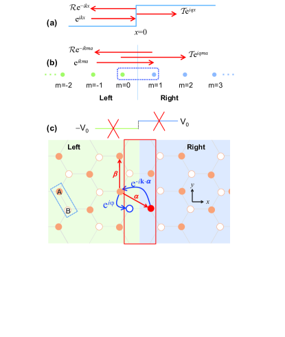
Interfacial hopping effect. We begin with the scattering of a one-dimensional free electron with mass and incident energy by a sharp interface to introduce the mode-matching method in the lattice model Ando (1991); Zhang and Yang (2018a) and the concept of interfacial hopping, with for brevity. In the continuum model, the interface is described by a step-wise potential that vanishes on the left () and takes a constant value on the right (). As shown in Fig. 1(a), a right-going incident wave with produces a left-going reflection wave and a right-going transmission wave , where . The reflection and transmission amplitudes and are determined by the continuity of the scattering state and its derivative at the interface:
| (1a) | ||||
| (1b) | ||||
| For a one-dimensional atomic chain with nearest-neighbor distance and hopping energy (with ), the interface is described by a constant on-site energy on the left () and on the right (), as shown in Fig. 1(b). The scattering state emanating from an incident wave from the left satisfies the Schrödinger equation , which reduces to | ||||
| (2) |
on the left of the interface and
| (3) |
on the right. Equation (2) admits a right-going eigen-solution (i.e., the incident wave) and a left-going eigen-solution (i.e., the reflection wave), where is determined by and is the energy band dispersion of the left region. For each , Eq. (2) connects the central site to the neighboring sites and , so the two eigen-solutions to Eq. (2) remain valid in the penetration region [dashed box in Fig. 1(b)]. In other words, solving Eq. (2) gives the left-region scattering state , which penetrates into the site of the right region due to the hopping of the electron across the interface. Similarly, Eq. (3) admits a right-going eigen-solution (i.e., the transmission wave) and a left-going eigen-solutions (excluded by causality), where is determined by . Therefore, solving Eq. (3) gives the right-region scattering state , which penetrates into the site of the left region due to the interfacial hopping. The reflection and transmission amplitudes are determined by the continuity of in the penetration region ( and ):
| (4a) | ||||
| (4b) | ||||
Compared with the continuum model, the lattice model reveals two distinct effects: (i) Nonparabolicity/Anisotropy of the energy band , as opposed to the parabolic energy band in the continuum model; (ii) Interfacial hopping, which leads to the continuity of the wave function at two different sites and [Eq. (4)], as opposed to the continuity of the wave function and its derivative at the same location [Eq. (1)] in the continuum model. Both (i) and (ii) originate from the electron hopping on the discrete lattice: the sum of the on-site energy and the nearest-neighbor hopping gives the energy band dispersion , while the hopping from across the interface onto gives rise to the continuity of the wave function at and and hence the propagation phases of the incident, reflection, and transmission waves in Eq. (4). In the continuum limit , we can expand effect (i) up to the second order of and expand effect (ii) up to the first order to recover the continuum model. For finite (especially at high doping densities ), however, the high-order contributions from effects (i) and (ii) become equally important.
The results above can be extended to a general lattice with an arbitrary number of orth-normalized atomic orbitals (associated with the same or different atoms) in each unit cell. Let’s label a unit cell by its center location , use for the th orbital in the -th unit cell, for the on-site energy, and for the hopping matrix from the -th unit cell to the -th unit cell. Under the Bloch basis ( is the total number of unit cells), the Hamiltonian for a uniform lattice is . The eigenstate is the product of the propagation phase accompanying the electron hopping between different unit cells and the -component spinor . In a -dimensional Bravais lattice, an interface is a -dimensional plane. For simplicity, we assume that this interface is defined by different on-site energies (e.g., on one side of the interface and on the other side), similar to the one-dimensional atomic chain. In this case, we can choose the primitive vectors of the Bravais lattice such that lie inside this interface. Given an incident wave , the scattering state is on one side of the interface and on the other side, where labels the different reflection and transmission waves. If we consider electron hopping between neighboring unit cells only, then
| (5) |
and the continuity equations across the interface gives
| (6a) | ||||
| (6b) | ||||
| Equation (6) is a direct generalization of Eq. (4), e.g., Eqs. (6a) and (4a) [Eqs. (6b) and (4b)] come from the continuity equation on the unit cell at the left (right) neighborhood of the interface. Therefore, the electron hopping on the discrete lattice leads to two equally important effects: (i) The hopping between neighboring unit cells gives rise to the phase factors in the lattice Hamiltonian Eq. (5) and hence energy band nonparabolicity/anisotropy. (ii) The hopping across the interface leads to wave function continuity at two different unit cells across the interface and hence the propagation phase factors , , in Eq. (6) – the interfacial hopping effect. For many years, the influence of (i) on various material properties have received widespread attention and intense efforts have been devoted to incorporating them into continuum models Bir and Pikus (1974); Winkler (2003). By contrast, effect (ii) is unique to the lattice model and we are not aware of any quantitative discussion about its influence on mesoscopic transport. | ||||
Tilted Klein tunneling across atomically sharp graphene junction. Atomically-sharp graphene junction was fabricated Bai et al. (2018) and studied numerically Liu et al. (2012); Logemann et al. (2015). Here we use this system to demonstrate the interfacial hopping effect in transport. As shown in Fig. 1(c), graphene has a triangular Bravais lattice, with two carbon atoms (marked by and ) in one unit cell and the carbon-carbon bond length nm. Uniform graphene described by the tight-binding model with nearest-neighbor hopping admits a conduction band with dispersion and a valence band with dispersion , where eV is the nearest-neighbor hopping energy Castro Neto et al. (2009), , and , are primitive Bravais vectors, as indicated by the red arrows in Fig. 1(c). Since vanishes at two inequivalent points and in the reciprocal space, the energy bands of graphene are approximately described by a Dirac-like continuum-model near and . An electron with momentum and energy has a wave function (spinors always normalized to as a convention), where is a phase factor. To eliminate unwanted intervalley scattering Urban et al. (2011) and focus on the interfacial hopping, we take the junction along the zigzag direction (defined as the axis for clarity), then an incident wave in one valley only produces reflection and transmission waves in the same valley. The junction potential is described by a constant on-site energy () for all the carbon sites in the left (right) region Zhang et al. (2017b); Zhang and Yang (2018a) [see the upper panel of Fig. 1(c)]. The Fermi energy determines the dimensionless doping level for the left region and for the right region: a positive (negative) doping level corresponds to electron or N (hole or P) doping, e.g., positive (negative) and describe N-N (P-P) junction, while positive and negative or vice versa describe P-N junctions.
We consider the scattering of an incident wave with energy and momentum on the left region. Given and , is uniquely determined by and the requirement that the group velocity of the incident wave has a positive projection along the axis. The translational invariance along the interface ( axis) leads to the conservation of , so the incident wave produces a left-going reflection wave with momentum [since is an even function of ] and a right-going transmission wave with momentum , where is uniquely determined by and the requirement that the group velocity of the transmission wave has a positive projection along the axis. In addition to these traveling waves, graphene also supports ideal evanescent waves. Fortunately, the latter do not affect the scattering across a sharp zigzag junction and hence can be discarded Zhang and Yang (2018a) as long as we employ the wave function continuity in the penetration region [red solid square in Fig. 1(c)]. On the left, including the penetration region, the scattering state
is the sum of the incident wave and the reflection wave. On the right, including the penetration region, the scattering state
is the transmission wave, where , , and . With the origin of the coordinate set on the atom [filled red circle in Fig. 1(c)] in the penetration region, the continuity of the scattering state on this atom gives , while the continuity of the scattering state on the atom [empty blue circle in Fig. 1(c)] gives where is the primitive vector of the graphene lattice [see the red arrow Fig. 1(c)]. Here () accounts for the relative phase between atoms in the same unit cell, while are propagation phase factors accompanying the electron hopping across the interface [see the blue arrow in Fig. 1(c)], i.e., interfacial hopping, which is absent in any continuum model. The continuity of the wave function in the penetration region can be written concisely as
| (7) |
which is a special case of Eq. (6). The condition for zero reflection or equivalently perfect transmission (i.e., and ) is
| (8) |
The left hand side is affected by the energy band nonparabolicity and anisotropy, while the right hand side accounts for the interfacial hopping. Due to the mirror symmetry of the junction about the axis [see Fig. 1(c)], the reflection probability is an even function of , so we need only consider the valley (i.e., ) and obtain
| (9) |
When the doping level is well below the Van Hove singularity (), we can use and with being the reduced momentum to obtain , so perfect transmission occurs at a tilted incident angle 222The incident (transmission) angle is the polar angle of the incident (transmission) group velocity about the axis. In general, this differs from that of the incident (transmission) momentum. When the doping level lies well below the Van Hove singularity of the graphene energy band, however, we can neglect this small difference, so that the polar angle of the reduced momentum is parallel (anti-parallel) to the polar angle of the group velocity.
| (10) |
where is the Fermi wavelength in the right (i.e., transmission) region. The corresponding transmission angle is obtained from the Snell’s law , which follows from the conservation of across the junction.
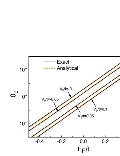
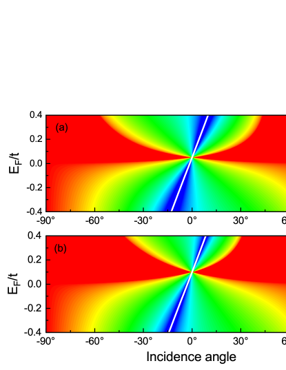
Equation (10) is valid for P-N, N-N, and P-P junctions, which correspond to , , and , respectively. As shown in Fig. 2, the analytical expression Eq. (10) agrees well with the exact numerical results over a wide doping level well beyond the linear Dirac regime, as long as the doping level lies below the Van Hove singularity. In contrast to the well-known Klein tunneling at normal incidence () Katsnelson et al. (2006); Allain and Fuchs (2011), Eq. (10) shows that zero reflection or equivalently perfect transmission across an atomically sharp graphene junction requires a tilted incidence angle that is uniquely determined by the dimensionless doping level on the transmission region. This phenomenon becomes very important when the Fermi wave length in the transmission region is comparable to the atomic distance . In Figs. 2(a) and 2(b), we show the contour plot for the reflection probability as a function of the Fermi energy and the incidence angle for two different junction potentials and . The tilted incident angle (as marked by the white solid lines) shows pronounced deviation from normal incidence. Next we show that the interfacial hopping plays an important role in this phenomenon.
Breaking pseudospin conservation by interfacial hopping. To understand the physical origin of the tilted Klein tunneling in the lattice model, we recall that in the linear continuum model Katsnelson et al. (2006); Allain and Fuchs (2011), the Hamiltonian of uniform graphene is and the eigenstates are , where is the azimuth angle of the reduced momentum . The spinor describes a pseudospin lying in the plane with an azimuth angle . In this model, the scattering state across the junction is given by on the left side and on the right side, where (). The continuity of the scattering state across the interface at gives
which resembles its lattice counterpart [Eq. (7)] ( approaches when approaches ), but does not carry the interfacial hopping phase . As a result, in the continuum model, perfect transmission requires or equivalently the pseudospin of the incident wave being parallel to that of the transmission wave, which is satisfied upon normal incidence (i.e., ). By contrast, in the lattice model, the perfect transmission condition requires Eq. (8), which is not satisfied upon normal incidence (e.g., ). This is because in the continuum model, the continuity equation for the scattering wave function occurs at the same location – the interface, while in the lattice model, the continuity equation occurs at two different unit cells across the interface – the interfacial hopping effect. Despite the same momentum conservation along the interface in both the continuum model and the lattice model, the unique interfacial hopping effect in the lattice model leads to the breakdown of the pseudospin conservation and hence the conventional Klein tunneling.
In Eq. (8), the nonparabolicity and anisotropy of the graphene energy band influences the values of the momenta , , and the spinor phases . This effect can be well incorporated by using more sophisticated continuum models, e.g., by adding higher-order terms or using more energy bands in the Hamiltonian. By contrast, the interfacial hopping phases and in the continuity equation cannot be incorporated into the continuum model. If we fully incorporate the former by using the exact momenta , , and spinor phases from the tight-binding model, but neglect the latter by replacing the right hand side of Eq. (8) with unity, then perfect transmission occurs at
as opposed to Eq. (9). When the doping level is well below the Van Hove singularity, the critical incident angle would be , which is opposite to the correct result in Eq. (10). This suggests that the interfacial hopping dominates over the nonparabolicity/anisotropy of the energy band. As the interfacial hopping is unique to the lattice model, this phenomenon differs qualitatively from existing electron-optics phenomena Cheianov et al. (2007); Lee et al. (2015); Chen et al. (2016); Williams et al. (2011); Beenakker et al. (2009); Wu et al. (2011); Zhai and Chang (2008); Li et al. (2017); Nguyen and Charlier (2018); Zhang and Yang (2018b) describable by continuum models.
Discussions. The critical incidence angle is completely determined by the dimensionless doping level in the transmission region, while the corresponding transmission angle is completely determined by in the incidence region. With the recently fabricated atomically sharp graphene P-N junction as an experimental platform Bai et al. (2018), both and can be tuned via the standard electrostatic doping technique Ahn et al. (2006), which has been widely used for graphene and other two-dimensional materials. Experimentally, the potential across an atomically sharp junction can reach (see Ref. Bai et al. (2018)) and the uniform doping level can reach the Van Hove singularity (i.e., ) (see Ref. Dombrowski et al. (2017)). For a rough estimate, we take and , then and the critical incident angle is . This strong deviation of from normal incidence (see Fig. 3) should be resolvable in multiprobe scanning tunneling microscopy Settnes et al. (2014) (see Refs. Nakayama et al. (2012); Li et al. (2013) for recent reviews) or in transverse magnetic focusing measurements Chen et al. (2016).
Another candidate experimental platform to observe this phenomenon is the “photonic graphene” Rechtsman et al. (2012); Plotnik et al. (2013), an array of evanescently coupled waveguides arranged in a honeycomb-lattice configuration Bahat-Treidel et al. (2010); Plotnik et al. (2013) (see Ref. Polini et al. (2013) for a review). Each waveguide has a single bound state, so the diffraction of light in this structure is described by the same tight-binding model as graphene. Here each waveguide mode corresponds to an atom and the tunneling between neighboring waveguides corresponds to the hopping between neighboring atoms. Importantly, the structure of the photonic lattice can be designed at will and is not subject to structural defects or absorbate contamination, so photonic graphene provides a platform for graphene physics not easily accessible otherwise. In particular, the distance between neighboring waveguides (corresponding to the atomic distance in the honeycomb lattice) can be easily made comparable to the wavelength of the photons, so that the critical incident angle deviates strongly from normal incidence, making the observation of this phenomenon feasible.
To summarize, for many years, the crucial roles of the energy band nonparabolicity/anisotropy and their incorporation into the continuum model has attracted a lot of attention. Here our work have identified the interfacial hopping effect as a missing ingredient that could be equally important as the energy band nonparabolicity/anisotropy for transport across atomically sharp interfaces, but it cannot be incorporated into the continuum model. The interfacial hopping shares the same physical origin as the the energy band nonparabolicity/anisotropy, so it is universal for any solid-state materials. Specializing to the honeycomb lattice of graphene reveals the breakdown of the well-known Klein tunneling and the onset of tilted Klein tunneling. We expect significant influence of the interfacial hopping effect on mesoscopic transport in other high-mobility materials at high carrier densities.
Acknowledgements. This work was supported by the National Key RD Program of China (Grant No. 2017YFA0303400), the NSFC (Grants No. 11504018, 11774021, and 11434010), and the NSFC program for “Scientific Research Center” (Grant No. U1530401). We acknowledge the computational support from the Beijing Computational Science Research Center (CSRC).
Author contributions. S.H.Z., W.Y., and K.C. conceived the idea. S.H.Z. and W.Y. formulated the theory, carried out the calculations, and wrote the paper. All authors commented on the manuscript.
Competing interests: The authors declare no competing interests.
References
- Spector et al. (1990) J. Spector, H. L. Stormer, K. W. Baldwin, L. N. Pfeiffer, and K. W. West, Appl. Phys. Lett. 56, 1290 (1990).
- Datta (1995) S. Datta, Electronic Transport in Mesoscopic Systems (Cambridge University Press, Cambridge, England, 1995).
- Cheianov et al. (2007) V. V. Cheianov, V. Fal’ko, and B. L. Altshuler, Science 315, 1252 (2007).
- Lee et al. (2015) G.-H. Lee, G.-H. Park, and H.-J. Lee, Nat. Phys. 11, 925 (2015).
- Chen et al. (2016) S. Chen, Z. Han, M. M. Elahi, K. M. M. Habib, L. Wang, B. Wen, Y. Gao, T. Taniguchi, K. Watanabe, J. Hone, et al., Science 353, 1522 (2016).
- Zhang et al. (2016) S.-H. Zhang, J.-J. Zhu, W. Yang, H.-Q. Lin, and K. Chang, Phys. Rev. B 94, 085408 (2016).
- Zhang et al. (2017a) S.-H. Zhang, J.-J. Zhu, W. Yang, and K. Chang, 2D Materials 4, 035005 (2017a).
- Williams et al. (2011) J. R. Williams, T. Low, M. S. Lundstrom, and C. M. Marcus, Nat Nano 6, 222 (2011).
- Beenakker et al. (2009) C. W. J. Beenakker, R. A. Sepkhanov, A. R. Akhmerov, and J. Tworzydło, Phys. Rev. Lett. 102, 146804 (2009).
- Wu et al. (2011) Z. Wu, F. Zhai, F. M. Peeters, H. Q. Xu, and K. Chang, Phys. Rev. Lett. 106, 176802 (2011).
- Castro Neto et al. (2009) A. H. Castro Neto, F. Guinea, N. M. R. Peres, K. S. Novoselov, and A. K. Geim, Rev. Mod. Phys. 81, 109 (2009).
- Mourik et al. (2012) V. Mourik, K. Zuo, S. M. Frolov, S. R. Plissard, E. P. A. M. Bakkers, and L. P. Kouwenhoven, Science 336, 1003 (2012).
- Nadj-Perge et al. (2014) S. Nadj-Perge, I. K. Drozdov, J. Li, H. Chen, S. Jeon, J. Seo, A. H. MacDonald, B. A. Bernevig, and A. Yazdani, Science 346, 602 (2014).
- Lv et al. (2015) B. Q. Lv, H. M. Xu, N.and Weng, J. Z. Ma, P. Richard, X. C. Huang, L. X. Zhao, G. F. Chen, C. E. Matt, F. Bisti, V. N. Strocov, et al., Nat. Phys. 11, 724 (2015).
- Xu et al. (2015a) S.-Y. Xu, N. Alidoust, I. Belopolski, Z. Yuan, G. Bian, T.-R. Chang, H. Zheng, V. N. Strocov, D. S. Sanchez, G. Chang, et al., Nat. Phys. 11, 748 (2015a).
- Xu et al. (2015b) S.-Y. Xu, I. Belopolski, N. Alidoust, M. Neupane, G. Bian, C. Zhang, R. Sankar, G. Chang, Z. Yuan, C.-C. Lee, et al., Science 349, 613 (2015b), ISSN 0036-8075.
- Hirschberger et al. (2016) M. Hirschberger, S. Kushwaha, Z. Wang, Q. Gibson, S. Liang, C. Belvin, B. Bernevig, R. Cava, and N. Ong, Nat. Mater. 15, 1161 (2016).
- Liu et al. (2014a) Z. K. Liu, J. Jiang, B. Zhou, Z. J. Wang, Y. Zhang, H. M. Weng, D. Prabhakaran, S.-K. Mo, H. Peng, P. Dudin, et al., Nat. Mater. 13, 677 (2014a).
- Liu et al. (2014b) Z. K. Liu, B. Zhou, Y. Zhang, Z. J. Wang, H. M. Weng, D. Prabhakaran, S.-K. Mo, Z. X. Shen, Z. Fang, X. Dai, et al., Science 343, 864 (2014b).
- Xiong et al. (2015) J. Xiong, S. K. Kushwaha, T. Liang, J. W. Krizan, M. Hirschberger, W. Wang, R. J. Cava, and N. P. Ong, Science 350, 413 (2015).
- Bradlyn et al. (2016) B. Bradlyn, J. Cano, Z. Wang, M. G. Vergniory, C. Felser, R. J. Cava, and B. A. Bernevig, Science 353, 558 (2016).
- Bradlyn et al. (2017) B. Bradlyn, L. Elcoro, J. Cano, M. G. Vergniory, Z. Wang, C. Felser, M. I. Aroyo, and B. A. Bernevig, Nature 547, 298 C305 (2017).
- Bir and Pikus (1974) G. Bir and G. Pikus, Symmetry and Strain-induced Effects in Semiconductors (Wiley, New York, 1974).
- Winkler (2003) R. Winkler, Spin-orbit Coupling Effects in Two-Dimensional Electron and Hole Systems (Springer-Verlag, Berlin, 2003).
- Wang et al. (2013) Y. H. Wang, H. Steinberg, P. Jarillo-Herrero, and N. Gedik, Science 342, 453 (2013).
- Baringhaus et al. (2014) J. Baringhaus, M. Ruan, F. Edler, A. Tejeda, M. Sicot, Taleb-IbrahimiAmina, A.-P. Li, Z. Jiang, E. H. Conrad, C. Berger, et al., Nature 506, 349 (2014).
- Jiang et al. (2013) Y. Jiang, T. Low, K. Chang, M. I. Katsnelson, and F. Guinea, Phys. Rev. Lett. 110, 046601 (2013).
- Katsnelson et al. (2006) M. I. Katsnelson, K. S. Novoselov, and A. K. Geim, Nat. Phys. 2, 620 (2006).
- Young and Kim (2009) A. F. Young and P. Kim, Nat. Phys. 5, 222 (2009).
- Stander et al. (2009) N. Stander, B. Huard, and D. Goldhaber-Gordon, Phys. Rev. Lett. 102, 026807 (2009).
- Allain and Fuchs (2011) P. E. Allain and J. Fuchs, The European Physical Journal B 83, 301 (2011).
- Katsnelson (2012) M. I. Katsnelson, Graphene: Carbon in Two Dimensions (Cambridge University Press, New York, 2012).
- Cheianov and Fal’ko (2006) V. V. Cheianov and V. I. Fal’ko, Phys. Rev. B 74, 041403 (2006).
- Bai et al. (2018) K.-K. Bai, J.-J. Zhou, Y.-C. Wei, J.-B. Qiao, Y.-W. Liu, H.-W. Liu, H. Jiang, and L. He, Phys. Rev. B 97, 045413 (2018).
- Note (1) Note1, the discrepancy between the tight-binding model and the continuum model has been noted in earlier works Tang et al. (2008); Liu et al. (2012). However, they only consider normal incidence and low doping (i.e., electron wavelength atomic distance), so the discrepancy is very small (less than 0.5%) and hence taken to be negligible Liu et al. (2012).
- Dombrowski et al. (2017) D. Dombrowski, W. Jolie, M. Petrović, S. Runte, F. Craes, J. Klinkhammer, M. Kralj, P. Lazić, E. Sela, and C. Busse, Phys. Rev. Lett. 118, 116401 (2017).
- Nakayama et al. (2012) T. Nakayama, O. Kubo, Y. Shingaya, S. Higuchi, T. Hasegawa, C.-S. Jiang, T. Okuda, Y. Kuwahara, K. Takami, and M. Aono, Advanced Materials 24, 1675 (2012).
- Li et al. (2013) A.-P. Li, K. W. Clark, X.-G. Zhang, and A. P. Baddorf, Adv. Funct. Mater. 23, 2509 (2013).
- Settnes et al. (2014) M. Settnes, S. R. Power, D. H. Petersen, and A.-P. Jauho, Phys. Rev. Lett. 112, 096801 (2014).
- Rechtsman et al. (2012) M. C. Rechtsman, J. M. Zeuner, A. Tünnermann, S. Nolte, M. Segev, and A. Szameit, Nat. Photon. 7, 153 (2012).
- Plotnik et al. (2013) Y. Plotnik, M. C. Rechtsman, D. Song, M. Heinrich, J. M. Zeuner, S. Nolte, Y. Lumer, N. Malkova, J. Xu, A. Szameit, et al., Nat. Mater. 13, 57 (2013).
- Ando (1991) T. Ando, Phys. Rev. B 44, 8017 (1991).
- Zhang and Yang (2018a) S.-H. Zhang and W. Yang, Phys. Rev. B 97, 035420 (2018a).
- Liu et al. (2012) M.-H. Liu, J. Bundesmann, and K. Richter, Phys. Rev. B 85, 085406 (2012).
- Logemann et al. (2015) R. Logemann, K. J. A. Reijnders, T. Tudorovskiy, M. I. Katsnelson, and S. Yuan, Phys. Rev. B 91, 045420 (2015).
- Urban et al. (2011) D. F. Urban, D. Bercioux, M. Wimmer, and W. Häusler, Phys. Rev. B 84, 115136 (2011).
- Zhang et al. (2017b) S.-H. Zhang, W. Yang, and K. Chang, Phys. Rev. B 95, 075421 (2017b).
- Note (2) Note2, the incident (transmission) angle is the polar angle of the incident (transmission) group velocity about the axis. In general, this differs from that of the incident (transmission) momentum. When the doping level lies well below the Van Hove singularity of the graphene energy band, however, we can neglect this small difference, so that the polar angle of the reduced momentum is parallel (anti-parallel) to the polar angle of the group velocity.
- Zhai and Chang (2008) F. Zhai and K. Chang, Phys. Rev. B 77, 113409 (2008).
- Li et al. (2017) Z. Li, T. Cao, M. Wu, and S. G. Louie, Nano Lett. 17, 2280 (2017), ISSN 1530-6984.
- Nguyen and Charlier (2018) V. H. Nguyen and J.-C. Charlier, Phys. Rev. B 97, 235113 (2018).
- Zhang and Yang (2018b) S.-H. Zhang and W. Yang, Phys. Rev. B 97, 235440 (2018b).
- Ahn et al. (2006) C. H. Ahn, A. Bhattacharya, M. Di Ventra, J. N. Eckstein, C. D. Frisbie, M. E. Gershenson, A. M. Goldman, I. H. Inoue, J. Mannhart, A. J. Millis, et al., Rev. Mod. Phys. 78, 1185 (2006).
- Bahat-Treidel et al. (2010) O. Bahat-Treidel, O. Peleg, M. Grobman, N. Shapira, M. Segev, and T. Pereg-Barnea, Phys. Rev. Lett. 104, 063901 (2010).
- Polini et al. (2013) M. Polini, F. Guinea, M. Lewenstein, H. C. Manoharan, and V. Pellegrini, Nat Nano 8, 625 (2013).
- Tang et al. (2008) C. Tang, Y. Zheng, G. Li, and L. Li, Solid State Commun. 148, 455 (2008), ISSN 0038-1098.