Ground-state spin blockade in a single-molecule junction
Abstract
It is known that the quantum-mechanical ground state of a nano-scale junction has a significant impact on its electrical transport properties. This becomes particularly important in transistors consisting of a single molecule. Due to strong electron-electron interactions and the possibility to access ground states with high spins, these systems are eligible hosts of a current-blockade phenomenon called ground-state spin blockade. This effect arises from the inability of a charge carrier to account for the spin difference required to enter the junction, as that process would violate the spin selection rules. Here, we present a direct experimental demonstration of ground-state spin blockade in a high-spin single-molecule transistor. The measured transport characteristics of this device exhibit a complete suppression of resonant transport due to a ground-state spin difference of 3/2 between subsequent charge states. Strikingly, the blockade can be reversibly lifted by driving the system through a magnetic ground-state transition in one charge state, using the tunability offered by both magnetic and electric fields.
Blockade mechanisms in charge transport involve various physical phenomena: The current in double quantum dots can be inhibited by the Pauli exclusion principle Koppens et al. (2005); Johnson et al. (2005); Liu et al. (2008), vibrational transitions in molecular junctions and quantum dots can be suppressed by Franck-Condon blockade Koch and von Oppen (2005); Leturcq et al. (2009); Burzurí et al. (2014), and in junctions with superconducting electrodes there may be no low-energy transport as a result of the superconducting energy gap Winkelmann et al. (2009); Deng et al. (2016). These blockade mechanisms all occur in combination with Coulomb blockade, which results from the energy level spacing and the energy costs of charging a weakly-coupled nano-object, i.e., the charging energy . Coulomb blockade can be overcome as soon as the energy of an electron in one electrode exceeds the addition energy . Then, electrons can sequentially travel from one electrode to the other via the nano-object. In every sequential electron tunneling (SET) event, the charge of the object changes by an elementary charge and the spin typically by 1/2, due to the added or removed electron.
Here, we study an exceptionally clear manifestation of the blockade phenomenon that occurs when the ground-state spin of subsequent charge states differs by more than 1/2. SET transitions between these ground states are forbidden by the spin selection rules and Coulomb blockade peaks are suppressed Weinmann et al. (1995); Heersche et al. (2006); Gaudenzi et al. (2017). We refer to this effect as ground-state spin blockade (GSSB). One of the necessary requirements for GSSB is a high-spin ground state, i.e., , in one of the charge states. This requirement is hard to obtain for top-down quantum dots and in the few earlier demonstrations of GSSB, neither the full suppression of the Coulomb blockade peaks nor control over the blockade was achieved Rokhinson et al. (2001); Hüttel et al. (2003). For molecules, high-spin ground states can be tailored by chemical design, making them promising candidates for observing GSSB. In this transport study, we provide experimental evidence for complete GSSB in a high-spin single-molecule junction. With an external magnetic field, the blockade can be reversibly lifted by driving the molecule in one charge state through a magnetic ground-state transition. The presence of GSSB puts constraints on the allowed transitions and is used as a diagnostic tool to determine the ground state, and excited states of the molecule.
The measurements were carried out with the device sketched in Fig. 1a. A single molecule is embedded in a circuit with two gold electrodes in which DC current () is measured as a function of the applied voltage difference between the electrodes (the bias voltage ) and the voltage applied to a capacitively coupled gate electrode (). The junction is formed by room-temperature electromigration Park et al. (1999) and self-breaking O’Neill and Van der Zant (2007) of a gold nanowire. A dilute solution of the molecules is dropcasted on a chip with 24 electromigrated junctions on which, after pumping away the solution and cooling down the sample, three junctions show Coulomb blockade with addition energies in the typical regime of molecular junctions, i.e., meV. The tunnel couplings and energy level alignments cannot be controlled by this technique and depend on the way the molecule is trapped inside the junction. One of the three samples shows the right combination of a small tunnel coupling, which allows for high-resolution spectroscopy, and a level alignment close to the Fermi level of the electrodes, such that the molecule can be charged within the accessible gate voltage range. All measurements shown here are of this particular junction and are taken at 40 mK in a dilution refrigerator.
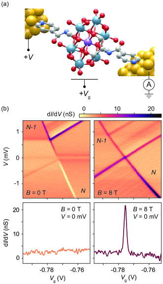
The molecule in the junction is a pyridine-functionalized Mn(III) Anderson polyoxometalate (POM) Allain et al. (2008), which is sketched in Fig. 1a. It consists of a molecular metal oxide formed by a central Mn(III)-ion, surrounded by six edge-sharing octahedra, which confer robustness to the POM and magnetic isolation. This type of molecule is axially functionalized on both sides by organic molecules linked directly to the Mn(III)-ion through alcoxo bridges. Magnetic characterization of these compounds in the solid state shows that the Mn(III) has a total spin and a g-factor close to 2 Abhervé et al. (2015) (see Supplemental Material for more details on the synthesis of the molecule).
In Fig. 1b, the two top panels show differential conductance (d/d) maps of the device as a function of and , at zero magnetic field and at 8 T. For clarity, we first discuss the map at 8 T, which looks like a common d/d map of a Coulomb-blockaded system containing a single object, here, a molecule. The regions labeled and are regions in which the charge of the molecule is fixed and SET processes are suppressed. Inside these regions, transport is governed by co-tunneling (COT) processes, which appear as horizontal lines. The two slanted lines that form the cross-like shape are the edges of the Coulomb diamonds and their point of incidence at zero bias is the charge degeneracy point. The bottom right panel shows that this point appears as a peak in the linear-conductance gate trace, i.e., the d/d as a function of . Looking for peaks in these traces is typically the first step to check whether a molecule is present in the junction. In the top and bottom regions of the d/d map, the charge of the molecule can fluctuate, allowing for SET processes to occur. The top SET region contains slanted lines starting from the left Coulomb edge at mV and, less intense, at mV, both moving towards the top right. These lines correspond to SET processes involving excited states.
Remarkably, in the map at 0 T, the charge degeneracy point is absent: slanted lines are present, but they do not cross at zero bias. At any gate voltage, the linear conductance is suppressed and only SET lines at finite voltages are present. This shows that transitions between the ground state of and the ground state of are blocked. The complete suppression can be seen more clearly in the zero-bias trace presented in the corresponding bottom panel, which in contrast to the 8 T trace shows no peak, or any other molecular signature. All the slanted lines in the map appear at finite bias voltages and mark transitions involving at least one excited state: The SET line starting at mV coincides with a COT line at that same bias voltage, which implies that their excitation energies are equal, and involve the same excited state. Similarly, the COT lines at mV in connect to two SET lines starting at the same bias voltages. Another faint COT line appears at mV in , closer to zero bias than its counterpart at positive bias. This asymmetry suggests that the corresponding excitation energy is influenced by the bias voltage, as will be discussed below. The region also contains a zero-bias line that resembles a Kondo resonance Liang et al. (2002), resulting from a degenerate ground state.
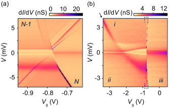
The striking difference between the maps at 0 T and at 8 T in Fig. 1b is the presence of the charge degeneracy point; the complete suppression of this point at 0 T is completely lifted at 8 T. To study the blockade mechanism in more detail, we show two d/d maps in a larger gate and bias-voltage range in Fig. 2, both recorded at 0 T. In Fig. 2a, the same features as in Fig. 1b can be observed, along with a broad horizontal line at mV and additional SET excitation lines at higher bias voltages. The Coulomb edges at negative bias change slope at the two coincidences with the broad horizontal line. This feature shows striking similarities with the simulated transport data presented in Stevanato et al. (2012), where a singlet-triplet ground-state transition line in a double-quantum-dot model is studied. The energies of the ground states separated by this line have a different dependence on bias voltage, causing their corresponding Coulomb edges to have different slopes.
The gate and bias-voltage dependence of the ground-state transition line is shown in Fig. 2b where the transport data is presented for an even wider gate-voltage range. The dashed brackets in this figure mark the gate-voltage range of Fig. 2a. Figure 2b reveals that the ground-state transition line, indicated by the arrow, extends towards positive bias voltages and has an anomalous parabolic shape; it can be well approximated by a function quadratic in and linear in (see Supplemental Material for a more detailed analysis of the ground-state transition line). Three regions with different ground states can be distinguished, separated by the parabola and the Coulomb edges. We label the regions , and , where and belong to the charge state , and to the charge state . In both and , a pair of COT lines appears at mV, symmetrically positioned around zero bias. In , a pair of gate-voltage dependent COT lines is present, starting at mV around V, moving away from zero bias as is increased. The excitation energy of this COT line thus depends on the gate voltage.
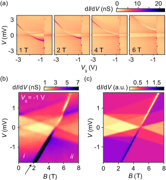
Next, we investigate the magnetic field dependence of the parabolic ground-state transition line. Figure 3a shows four maps in the same bias and gate voltage range as in Fig. 2b, at different magnetic fields. By increasing the magnetic field, the parabola moves towards higher bias voltages, and the d/d along the line changes in magnitude and sign. For an increasing part of the line, the d/d turns negative, i.e., the current goes down by increasing the bias voltage at the transition from to .
The fact that the ground-state transition line moves upwards with magnetic field implies that the total spin of the ground state in region is larger than in region ; upon increasing the magnetic field, the ground state with higher spin becomes energetically more favorable and the transition occurs at higher bias voltages. Above 4 T, region moves across zero bias at the charge degeneracy point, which lifts the GSSB at this point. The parabola thus marks the transition from a spin-blockaded region (), to a region where the blockade is lifted ().
To identify the spin states in we focus on the magnetic-field dependence of the d/d spectrum at a fixed gate voltage V (see Fig. 3b). The Kondo-like peak at zero bias splits linearly in two in a magnetic field, which verifies the presence of a degenerate ground state at 0 T. The COT excitations at mV and mV split in three and appear asymmetric in position and intensity. The fact that these excitations split in three implies that the corresponding excited state is a spin multiplet with a larger spin than the ground state; this can be deduced from the spin selection rules for COT processes Gaudenzi et al. (2017). Moreover, the spin selection rules impose additional constraints which lead to the conclusion that the spin difference between the excited state and the ground state is 1.
At about 5 T, one excitation from the excited spin multiplet crosses zero bias, which at that point becomes the new spin ground state. The two regions with different ground states are separated by the slanted line indicated by the arrow. These regions correspond to and in Fig. 2b, labeled accordingly in Fig 3b. The finite slope of the ground-state transition line results from the influence of the bias voltage on the associated excitation energy. This is also reflected by the asymmetry in bias voltage at which the multiplet excitations appear.
A model explaining the main features of the experimental data can now be constructed. The observed spin excitations occur at relatively low bias voltages ( 1 mV), which suggests that they are not related to spin reconfigurations of the Mn center itself, as for spin-crossover molecules Miyamachi et al. (2012); Meded et al. (2011); the energies of these transitions are typically orders of magnitude larger. Rather, we propose a model in which we invoke a weakly-coupled spin, exchange coupled to the high-spin center. This spin is possibly residing on the ligands of the molecule, as in other molecular systems Thiele et al. (2014); Osorio et al. (2009) and we will refer to it as the ligand spin. The low-energy COT excitations in this model are transitions in which the ligand spin is flipped with respect to the spin of the Mn center.
We simulate the spin-excitation spectra of this system by a tunneling model based on Ternes (2015). The result of the simulation is presented in Fig. 3c. The model includes COT processes of second order and solves the rate equations for a spin system consisting of a ligand spin , tunnel coupled to two reservoirs and exchange coupled to a high-spin () center. The exchange coupling in is anti-ferromagnetic, which at low magnetic fields results in a low-spin ground state () and a high-spin excited state (). We add a linear term in the expression of the exchange coupling as in Stevanato et al. (2012), which accounts for the asymmetric positions of the COT excitations and the appearance of the slanted ground-state transition line.
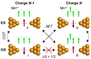
The ground state (GS) and excited state (ES) in the simulation of are sketched on the left-hand side in Fig. 4, where red arrows represent the ligand spins, green arrows the spins of the Mn center and yellow spheres the gold atoms of the electrodes. The right-hand side of Fig. 4 shows the GS and ES in . The observed SET and COT transitions between the states are indicated by the solid and dashed black arrows, respectively. In the transition from charge state to , the added electron is likely to reside on the metal center, changing the oxidation state from Mn4+ to Mn3+, as illustrated in Fig. 4. This charge transition of the Mn center occurs in solutions of this compound as shown by cyclic voltammetry measurements Allain et al. (2008). The spin of the Mn center in would then match the spin measured in crystals of this type of compound Abhervé et al. (2015), namely .
For GSSB to occur in this system, the ground-state spin should change by more than 1/2 upon charging. This can happen if the added charge not only contributes with its intrinsic spin, but its presence also changes the sign of the exchange coupling from anti-ferromagnetic to ferromagnetic, further increasing the total spin by 1. Such a transition of the exchange coupling is observed, and it is marked by the parabolic ground-state transition line in . The gate and bias-voltage dependence of this line shows that the exchange coupling is strongly influenced by the electric field, as was observed in other molecular systems Osorio et al. (2009); Roch et al. (2008).
We speculate that the observed tunability of the exchange coupling between the ligand spin and the spin of the Mn center follows from the influence of the gate and bias voltage on the spatial distribution of the ligand spin, which appears to be different for the two charge states: In , the ligand spin could be delocalized over the orbitals of the Mn3+, resulting in a ferromagnetic coupling with the state of the Mn+3 by Hund’s rule. In contrast, in the ligand spin may have no overlap with the orbitals of Mn4+ and it may be located near the orbitals to which it couples anti-ferromagnetically, as observed in .
The total spin of states and , as shown in Fig. 4, are 1 and 5/2, respectively, which amounts to a spin difference of 3/2. SET transitions between these ground states are thus rendered forbidden, as indicated by the red cross in Fig. 4. At high magnetic fields, the high-spin state () becomes the ground state for , lowering the ground-state spin difference to 1/2, whereby the GSSB is lifted.
This work shows that the act of charging a nano-scale object is not merely a consecutive filling of the lowest unoccupied orbitals, whereby the spin changes by 1/2. Rather, the act of charging can have a strong influence on the internal exchange couplings of the object, to a degree that ground-state transitions cannot be realized by single charge carriers. A thorough understanding of the resulting GSSB may therefore prove to be crucial in high-spin devices with applications in spintronics Bogani and Wernsdorfer (2010); Sanvito (2011); Clemente-Juan et al. (2012) and quantum computing Leuenberger and Loss (2001); Thiele et al. (2014); Shiddiq et al. (2016).
In summary, we have demonstrated GSSB in a single-molecule junction, which can be reversibly lifted by driving the system through a magnetic ground-state transition with an external magnetic field. The blockade results from a sign change of the exchange coupling upon charging, which causes the ground-state spin of subsequent charge states to differ by more than 1/2. This work demonstrates how the act of charging can induce a magnetic phase transition in a high-spin device by which resonant transport is completely suppressed.
Acknowledgements.
This work was supported by the Netherlands Organisation for Scientific Research (NWO/OCW), as part of the Frontiers of Nanoscience program, and the ERC Advanced Grant agreement numbers 240299 (Mols@Mols) and 788822 (Mol-2D). P.G. acknowledges a Marie Skłodowska-Curie Individual Fellowship under grant TherSpinMol (ID: 748642) from the European Union’s Horizon 2020 research and innovation programme. The work in Spain is supported by the Spanish MINECO (Unit os Excellence Maria de Maeztu MDM2015-0538 and Project MAT2017-89993-R co-financed by FEDER) and the Generalitat Valenciana (PROMETEO Programme). The Center for Quantum Devices is funded by the Danish National Research Foundation.References
- Koppens et al. (2005) F. H. L. Koppens, J. A. Folk, J. M. Elzerman, R. Hanson, L. H. W. Van Beveren, I. T. Vink, H.-P. Tranitz, W. Wegscheider, L. P. Kouwenhoven, and L. M. K. Vandersypen, Science 309, 1346 (2005).
- Johnson et al. (2005) A. C. Johnson, J. R. Petta, C. M. Marcus, M. P. Hanson, and A. C. Gossard, Physical Review B 72, 165308 (2005).
- Liu et al. (2008) H. W. Liu, T. Fujisawa, Y. Ono, H. Inokawa, A. Fujiwara, K. Takashina, and Y. Hirayama, Physical Review B 77, 073310 (2008).
- Koch and von Oppen (2005) J. Koch and F. von Oppen, Physical Review Letters 94, 206804 (2005).
- Leturcq et al. (2009) R. Leturcq, C. Stampfer, K. Inderbitzin, L. Durrer, C. Hierold, E. Mariani, M. G. Schultz, F. Von Oppen, and K. Ensslin, Nature Physics 5, 327 (2009).
- Burzurí et al. (2014) E. Burzurí, Y. Yamamoto, M. Warnock, X. Zhong, K. Park, A. Cornia, and H. S. J. van der Zant, Nano Letters 14, 3191 (2014).
- Winkelmann et al. (2009) C. B. Winkelmann, N. Roch, W. Wernsdorfer, V. Bouchiat, and F. Balestro, Nature Physics 5, 876 (2009).
- Deng et al. (2016) M. T. Deng, S. Vaitiekėnas, E. B. Hansen, J. Danon, M. Leijnse, K. Flensberg, J. Nygård, P. Krogstrup, and C. M. Marcus, Science 354, 1557 (2016).
- Weinmann et al. (1995) D. Weinmann, W. Häusler, and B. Kramer, Physical Review Letters 74, 984 (1995).
- Heersche et al. (2006) H. B. Heersche, Z. de Groot, J. A. Folk, H. S. J. van der Zant, C. Romeike, M. R. Wegewijs, L. Zobbi, D. Barreca, E. Tondello, and A. Cornia, Physical Review Letters 96, 206801 (2006).
- Gaudenzi et al. (2017) R. Gaudenzi, M. Misiorny, E. Burzurí, M. R. Wegewijs, and H. S. J. van der Zant, The Journal of Chemical Physics 146, 092330 (2017).
- Rokhinson et al. (2001) L. P. Rokhinson, L. J. Guo, S. Y. Chou, and D. C. Tsui, Physical Review B 63, 035321 (2001).
- Hüttel et al. (2003) A. K. Hüttel, H. Qin, A. W. Holleitner, R. H. Blick, K. Neumaier, D. Weinmann, K. Eberl, and J. P. Kotthaus, Europhysics Letters 62, 712 (2003).
- Park et al. (1999) H. Park, A. K. L. Lim, A. P. Alivisatos, J. Park, and P. L. McEuen, Applied Physics Letters 75, 301 (1999).
- O’Neill and Van der Zant (2007) E. A. O’Neill, K Osorio and H. S. J. Van der Zant, Applied Physics Letters 90, 133109 (2007).
- Allain et al. (2008) C. Allain, S. Favette, L.-M. Chamoreau, J. Vaissermann, L. Ruhlmann, and B. Hasenknopf, European Journal of Inorganic Chemistry 2008, 3433 (2008).
- Abhervé et al. (2015) A. Abhervé, M. Palacios-Corella, J. M. Clemente-Juan, R. Marx, P. Neugebauer, J. van Slageren, M. Clemente-León, and E. Coronado, Journal of Materials Chemistry C 3, 7936 (2015).
- Liang et al. (2002) W. Liang, M. P. Shores, M. Bockrath, J. R. Long, and H. Park, Nature 417, 725 (2002).
- Stevanato et al. (2012) C. Stevanato, M. Leijnse, K. Flensberg, and J. Paaske, Physical Review B 86, 165427 (2012).
- Miyamachi et al. (2012) T. Miyamachi, M. Gruber, V. Davesne, M. Bowen, S. Boukari, L. Joly, F. Scheurer, G. Rogez, T. K. Yamada, P. Ohresser, et al., Nature Communications 3, 938 (2012).
- Meded et al. (2011) V. Meded, A. Bagrets, K. Fink, R. Chandrasekar, M. Ruben, F. Evers, A. Bernand-Mantel, J. S. Seldenthuis, A. Beukman, and H. S. J. van der Zant, Physical Review B 83, 245415 (2011).
- Thiele et al. (2014) S. Thiele, F. Balestro, R. Ballou, S. Klyatskaya, M. Ruben, and W. Wernsdorfer, Science 344, 1135 (2014).
- Osorio et al. (2009) E. A. Osorio, K. Moth-Poulsen, H. S. J. van der Zant, J. Paaske, P. Hedegård, K. Flensberg, J. Bendix, and T. Bjørnholm, Nano Letters 10, 105 (2009).
- Ternes (2015) M. Ternes, New Journal of Physics 17, 063016 (2015).
- Roch et al. (2008) N. Roch, S. Florens, V. Bouchiat, W. Wernsdorfer, and F. Balestro, Nature 453, 633 (2008).
- Bogani and Wernsdorfer (2010) L. Bogani and W. Wernsdorfer, in Nanoscience And Technology: A Collection of Reviews from Nature Journals (World Scientific, 2010) pp. 194–201.
- Sanvito (2011) S. Sanvito, Chemical Society Reviews 40, 3336 (2011).
- Clemente-Juan et al. (2012) J. M. Clemente-Juan, E. Coronado, and A. Gaita-Ariño, Chemical Society Reviews 41, 7464 (2012).
- Leuenberger and Loss (2001) M. N. Leuenberger and D. Loss, Nature 410, 789 (2001).
- Shiddiq et al. (2016) M. Shiddiq, D. Komijani, Y. Duan, A. Gaita-Ariño, E. Coronado, and S. Hill, Nature 531, 348 (2016).