The Doping effect of Chalcogen on the Two-Dimensional
Ferromagnetic Material Chromium Tribromide
Abstract
Recently the discovery of magnetic order in two-dimensional monolayer chromium trihalides opens the new research field in two-dimensional materials. We use first-principles calculations to systematically examine the doping effect of chalcogen on CrBr3. In the case of S-doping, four stable configurations, Cr2Br5S, Cr2Br4S2-A, Cr2Br4S2-B and Cr2Br3S3-A, are predicted to be ferromagnetic semiconductors. It is found that the new bands appearing in the original bandgap are made up of S-p and Cr-d-eg orbits, lead to the obvious reduce of bandgap and the enhanced optical absorption in the visible range. Due to the decrease of valence electron after chalcogen doping, the magnetic moment also decreases with the increase of S atoms, and the character of ferromagnetic semiconductor is always hold in a wide range of strain. The results shown that monolayer CrBr3 with chalcogen doping supply a effectual way to control the magnetism and extend the optoelectronic applications.
I Introduction
In the last decade, two-dimensional (2D) materials Novoselov2005 ; Zhang2005 ; Geim2013 ; Kim2015 ; Xi2016 ; Saito2016 have attracted a great deal of attention also been one of the most exciting research fields due to the wealth of physics and promising applications. Besides the earliest graphene, various 2D materials also include hexagonal boron nitride, silicene, transition metal dichalcogenides, MXene and so on. However, the absent of intrinsic magnetism in the most of the available 2D materials with pristine form limits their applications in spintronics and spin-based electronics, particularly information technology. As a consequence, 2D ferromagnetic materials with the combination of large spin polarization and high Curie temperature (TC) are of particular importance and interest. The simple and direct means to achieve magnetic in 2D materials is dopants of magnetic atoms. However, doping not only destroys the perfect crystalline order, but also the low solubility and surface clustering Wang2005 ; Dietl2010 are the serious problems. Although there are some other strategies to magnetize Han2014 , the long-range magnetic order is rarely observed experimentally in 2D materials. For the theoretical reason, Mermin and Wagner theorem demonstrate the strong fluctuations lead to the absence of long range magnetic order in spin-rotational invariant systems with short range exchange interactions.
Fortunately, the magnetocrystalline anisotropy make some materials be not limited by the Mermin-Wagner theorem. The recent reports of magnetic order in different 2D crystals (Cr2Ge2Te6, CrI3 and FePS3) Gong2017 ; Huang2017 ; Wang2016 ; Lee2016 ; Wang2018 mark a milestone in the research of 2D magnetic materials and explore the 2D magnetic physics, indispensable for the low-dimensional spintronics. The small cleavage energy in the ferromagnetic van der Waals (vdW) bulk CrI3 is propitious to the mechanically exfoliated monolayer structure, prevalent in other common 2D materials. The magnetization experiments show the bulk crystal has the out-of-plane ferromagnetic (FM) order below TC = 68 K McGuire2015 ; Hansen1959 ; Dillon1965 with weak interlayer coupling. FM order is still residing in the monolayer structure with the lower TC of 45 K Huang2017 . But the suppressed magnetization occurs in the bilayer CrI3 due to the metamagnetic effect Stryjewski1977 . The numerous publications with regard to CrI3 emerge in order to study and manipulate the magnetic properties Klein2018 ; Song2018 ; Frisk2018 ; PeihengJiang2018 ; ChengxiHuang2018 . The temperature-dependent magnetic anisotropy Richter2018 of 2D CrI3 is contributed from the ferromagnetic super-exchange across the anisotropic Cr-I-Cr bonds and the weak single ion anisotropy of Cr atom Lado2017 . Furthermore, the electric field Huang2018 , electrostatic doping Jiang2018 and strain Zheng2018 are found to control the 2D magnetism of CrI3. Besides, the homogeneous materials CrBr3 and CrCl3 also induce the research interests Tsubokawa1960 ; Wang2011 ; Liu2016 ; Zhang2015 ; Abramchuk2018 ; Li2018 ; McGuire2017 and the bulk CrBr3 in particular has been studied as ferromagnetic semiconductor with Tc = 31 K long ago Tsubokawa1960 . And the in-plane multiferroicity ChengxiHuang2018 , such as ferromagnetic and ferroelectricity order, are also discovered in the charged monolayer CrBr3. The mixed halide series CrCl3-xBrx realizes the regulation of exchange anisotropy Abramchuk2018 and can be applied to the ultrathin magneto-optical devices Zhong2017 ; Wang2017 ; Seyler2018 .
In the present work, we focus on the 2D semiconductor CrBr3 and study the doping effect of chalcogen (S, Se and Te), in consideration of ferromagnetic metal in chromium chalcogens Lishuo2018 ; CongWang2018 with the same crystal structure as CrI3. Except the prototype structure of CrBr3, Six types of doping structure have been constructed with doping concentration of 1 3 chalcogenide atoms per primitive cell. In the case of Cr2Br6-xSx, four of the structures have dynamic stability, verified by the phonon spectra. They are as follows: Cr2Br5S, Cr2Br4S2-A, Cr2Br4S2-B and Cr2Br3S3-A. By calculating spin-polarized electronic structures, the four stable configurations are also confirmed as ferromagnetic semiconductor, coordination with CrBr3. However, there new bands appears in the bandgap of Cr-d-t2g orbit and the number of new bands increases linearly with S atomic content, which impact the global bandgap significantly. Due to the reduce of valence electron, magnetic moment also decreases under the doping condition, such as 3 per Cr2Br3S3-A primitive cell. These results suggest that monolayer CrBr3 with chalcogen doping is also robust intrinsic ferromagnetic semiconductor. Moreover, the new energy band can also absorb the low-energy photons and lead to the optical absorption in the visible range increases, which makes CrBr3 with chalcogen doping to be possible candidates for optoelectronic applications.
II Methods
Technical details of the calculations are as follows. All calculations of electronic structures and optical properties accurately were carried out using the Vienna ab initio simulation package (VASP) code Kresse19961 ; Kresse19962 within the projector augmented-wave (PAW) method Blochl1994 ; Kresse1999 and the exchange correlation functional of General gradient approximation (GGA) in the Perdew-Burke-Ernzerhof (PBE) implementation Perdew1996 . The thickness of the vacuum gap is at least 15 , which is large enough to avoid the interlayer interactions in the periodic structure. By requiring convergence of results, the kinetic energy cutoff of eV and the Monkhorst-Pack -mesh of 16161 were used in all calculations about the electronic ground-state properties. The phonon spectra was calculated on a 441 -grid using the density functional perturbation theory (DFPT) Baroni2001 with VASP and Phonopy codes Togo2008 . The biaxial strain was introduced by adjusting the lattice constant with the strain capacity = (-)/100 %, where is equilibrium lattice constant. The equilibrium lattice constant of the monolayer CrBr3 was found to be = 6.43 .
III Results
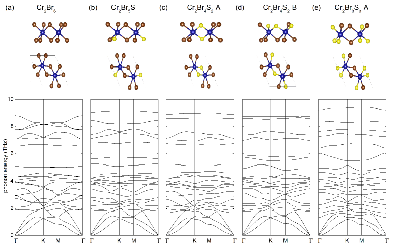
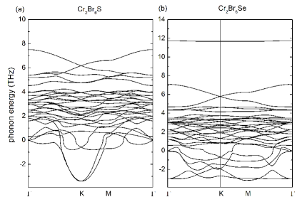
Now we discuss the possible lattice structures of Cr2Br6-xSx with = 13. First, the hexagonal honeycomb primitive cell of CrBr3 has eight atoms with each Cr surrounded by six Br atoms [Fig. 1(a)]. Due to the equivalency of six Br atoms in the primitive cell, Cr2Br5S has only one structure, as shown in Fig. 1(b). For the case of two S atoms, there are three different structures, marked by Cr2Br4S2-A [Fig. 1(c)], Cr2Br4S2-B [Fig. 1(d)] and Cr2Br4S2-C (see Appendix A) for simplicity, corresponding to the adjacency, alternation and para-position in the top-view of Cr2Br6-xSx, respectively. And there are two structures for the case of three S atoms. One is shown in Fig. 1(e) with three S atoms locating at the top and bottom edges of Cr atoms, Cr2Br3S3-A. The other one have three ipsilateral S atoms, Cr2Br3S3-B (see Appendix A), similar to the Janus monolayer structure of transition metal dichalcogenide Lu2017 . The doping of S atom lead to the slight decrease of equilibrium lattice constant, as shown in Tab. 1. Furthermore, the calculations of phonon spectra are applied to ensure the stability. The absent of imaginary frequency in the phonon spectrum of Cr2Br6 illustrates the dynamic stability of prototype structure, consistent with the previous works Zhang2015 . After the doping of S atom, it is found that not all cases have stability. Cr2Br5S, Cr2Br4S2-A, Cr2Br4S2-B and Cr2Br3S3-A are stable as shown in Fig. 1, contrary to the other cases (see Appendix A).
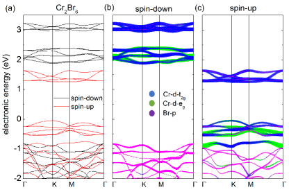
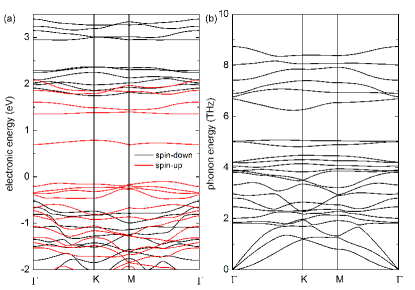
The results of electronic structure show that monolayer Cr2Br6 is ferromagnetic semiconductor with the bandgap of 1.32 eV [Fig. 2(a)], in coordination with the previous work Zhang2015 . The conduction band minimum (CBM) of band structure in the spin-down direction mainly consist of the d-t2g orbit of Cr atom as well as p orbit of Br atom contributing the valence band maximum (VBM) [Fig. 2(b)]. For the case of spin-up direction [Fig. 2(c)], CBM are also d-t2g orbit, but VBM is composed of d-t2g and d-eg orbits of Cr atom, clearly different from the spin-down direction. And the band structure of spin-up direction provides the global bandgap, much lower than that in spin-down direction [Tab. 1]. Due to the ferromagnetic semiconductor, integral magnetic moment is also obtained with the value of 6 per primitive cell [Tab. 1], which are from 3 of each Cr atom.
| bandgapup | bandgapdown | magnetic moment | |||
|---|---|---|---|---|---|
| (eV) | (eV) | (/ primitive cell) | |||
| Cr2Br6 | 6.43 | 1.32 | 2.72 | 6.0 | |
| Cr2Br5S | 6.37 | 0.79 | 2.29 | 5.0 | |
| Cr2Br4S2-A | 6.31 | 0.54 | 2.05 | 4.0 | |
| Cr2Br4S2-B | 6.32 | 0.44 | 1.93 | 4.0 | |
| Cr2Br3S3-A | 6.28 | 0.17 | 1.60 | 3.0 | |
| Cr2Br5Se | 6.36 | 0.79 | 2.27 | 5.0 |
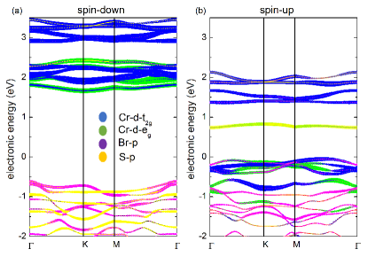
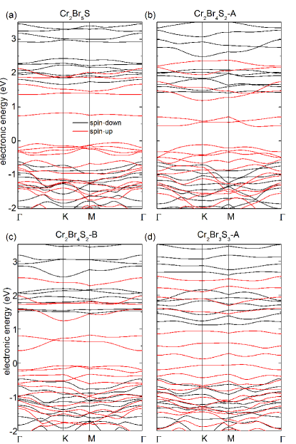
We then study the doping effect of S atom on the electronic structure of Cr2Br6. All the four stable structures of Cr2Br6-xSx have the ferromagnetic ground state as same as Cr2Br6 and the ferromagnetic band structure are shown in Fig. 3. It is obviously found that the global bandgap, spin-up direction, decreases rapidly with the increase in numbers of substitutional S atoms and reduces to a fairly low value of 0.17 eV in Cr2Br3S3-A. The reduce of bandgap also occurs in the case of spin-down direction, as summarized in Tab. 1. The projected band structures of Cr2Br5S show that S atom primarily influences the band structure in the spin-up direction [Fig. 4]. A new energy band presents in the energy gap between of Cr-d-t2g orbits and is contributed by the p orbit of S atom and d-eg orbit of Cr atom. The new bands in the energy range of 0 1 eV for other cases are all the results from the same reason. And the effect of S atoms is also reflected by the magnetic moment, which decreases linearly with increase of S atoms. For example, there are still 3 per Cr2Br3S3-A primitive cell [Tab. 1]. The main reason is that the decrease of valence electrons after S substitutions impact the occupation numbers on the magnetic Cr-d orbit. The results suggest that monolayer Cr2Br6-xSx are also robust intrinsic ferromagnetic semiconductor with different magnetic moments.
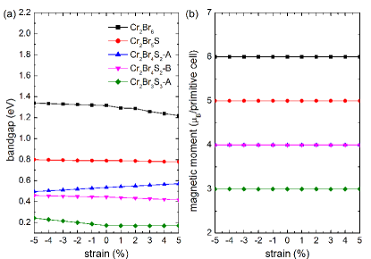
Because the possible lattice mismatching with the substrates in the different experimental preparations lead to the present of strain inevitably, the strain is also considered to study the stability of ferromagnetic semiconductor and the modulation of strain. The variation of bandgap under biaxial strains is displayed in Fig. 5(a). The bandgap of Cr2Br6-xSx is robust to the biaxial strain obviously, and the bandgap of Cr2Br5S has the minimum change. The result of magnetic moment also illustrates that Cr2Br6-xSx maintains the character of ferromagnetic semiconductor in a wide range of strain. Beyond S atom, we also consider the effect of heavier chalcogen (Se and Te) in the same structures as above. But it is found that only Cr2Br5Se has structural stability, as shown in Fig. 6, while imaginary frequency exists in other situations, as summarized in Tab. 2. The electronic structures show that Cr2Br5Se is also ferromagnetic semiconductor and has a bandgap close to Cr2Br5S. Similarly, the new band in the range of 0 1 eV also contributes from the Se-p and Cr-d-eg orbits.
| S | Se | Te | ||
|---|---|---|---|---|
| Cr2Br5X | stable | stable | -0.09 | |
| Cr2Br4X2-A | stable | -0.05 | -0.08 | |
| Cr2Br4X2-B | stable | -0.04 | -0.12 | |
| Cr2Br4X2-C | -0.32 | -0.03 | -0.12 | |
| Cr2Br3X3-A | stable | -0.07 | -0.09 | |
| Cr2Br3X3-B | -0.06 | -0.08 | -1.60 |
In addition, we have also calculated the doping effect on the optical properties of Cr2Br6 with chalcogen. As shown in Fig. 7(a), the in-plane isotropic optical absorption spectra of xy plane distinct from that along the z axis because of the hexagonal symmetry of Cr2Br6. The onset peak around 1.3 eV in Cr2Br6 can be traced back to the excitation from valence band to lowest conduction band in the spin-up subband [Fig. 2(c)]. And the most obvious result after the doping is the break of in-plane isotropy, as shown in Fig. 7(b-f), due to the position deviation of S or Se atom relative to Br atom in prototypical Cr2Br6 [Fig. 1]. Assisted by the new energy band in the original bandgap of spin-up subband, electronic transition can absorb the low-energy photons, so that the optical absorption of all doping cases in the visible range increases, especially Cr2Br4S2-A and Cr2Br3S3-A. This illustrates that Cr2Br6 with S and Se doping are possible candidates for optoelectronic applications.
IV Discussion
We have investigated the doping effect of chalcogen (S, Se and Te) on the CrBr3 using first-principles calculations. We now take Cr2Br6-xSx as the example to summarize our results. Four stable configurations are predicted to be ferromagnetic semiconductors: Cr2Br5S, Cr2Br4S2-A, Cr2Br4S2-B and Cr2Br3S3-A. After the doping of S atom, the new bands appearing in the energy range of 0 1 eV are made up of S-p and Cr-d-eg orbits and lead to the obvious reduce of bandgap in the spin-up direction. Since the change of valence electron, the magnetic moment also decreases with the increase of S atoms, such as Cr2Br3S3-A has the minimum magnetic moment of 3 per primitive cell. And the character of ferromagnetic semiconductor is always hold in a wide range of strain. Furthermore, the doping of chalcogen can also lead to the increase of optical absorption in the visible range and make it to be possible candidates for optoelectronic applications.
As an important material in FM semiconductor, CrI3 is considered certainly, but we do not find any stable structures, as shown in Appendix B. Except for the substitution, we also calculate the case of atomic adds because of the vacancy at the lattice vertex [Fig. 1]. The large imaginary frequency also explain the structural instability of Cr2Br6S and Cr2Br6Se (see Appendix C). For the unstable structures, especially the structures with very small imaginary frequency, such as the Janus Cr2Br3S3-B and Cr2I5S, maybe prepared in the experiments with the help of substrate, which can enhance 2D material stability. Importantly, we have shown that monolayer CrBr3 with chalcogen doping is also robust intrinsic ferromagnetic semiconductor and supply an effectual way to control the magnetism and optic properties of monolayer CrBr3, which is the current experiments desperately needed.
Acknowledgements.
This work was supported by the NSFC (Grants No.11747054 and No.11874113), the Specialized Research Fund for the Doctoral Program of Higher Education of China (Grant No.2018M631760), the Project of Heibei Educational Department, China (No. ZD2018015 and QN2018012), and the Advanced Postdoctoral Programs of Hebei Province (No.B2017003004).Appendix A Unstable structures of Cr2Br6-xSx
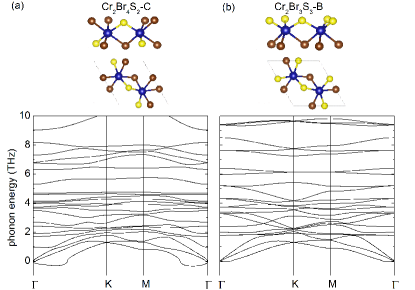
It is found that two of the crystal structures Cr2Br6-xSx considered in the present work are unstable, ensured by the imaginary frequency around point, as shown in Fig. A1. And the value of imaginary frequency in Cr2Br3S3-B is smaller than that of Cr2Br4S2-C as well as the distribution of imaginary frequency.
Appendix B Cr2I6-xSx
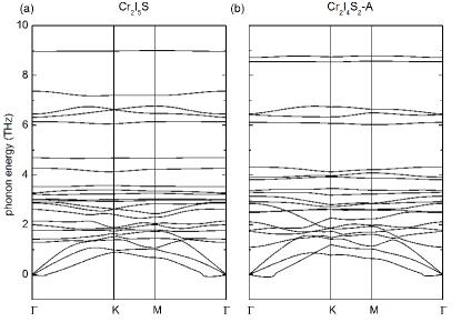
The doping effect of chalcogen is also calculated in the CrI3 system. But we haven’t obtained any stable structure and figure. A2 only plots the phonon spectra of Cr2I5S and Cr2I4S2-A with small imaginary frequency around point.
Appendix C Cr2Br6S and Cr2Br6Se
The addition of chalcogen is also calculated in the CrBr3 system. But there are large imaginary frequency in the phonon spectra, as shown in Fig. A3.
References
- (1) K. S. Novoselov, A. K. Geim, S. V. Morozov, D. Jiang, M. I. Katcnelson, I. V. Grigorieva, S. V. Dubonos, and A. A. Firsov, Nature 438, 197 (2005).
- (2) Y. Zhang, Y.-W. Tan, H. L. Stormer, and P. Kim, Nature 438, 201 (2005).
- (3) A. K. Geim and I. V. Grigorieva, Nature 499, 419 (2013).
- (4) J. Kim, S. S. Baik, S. H. Ryu, Y. Sohn, S. Park, B.-G. Park, J. Denlinger, Y. Yi, H. J. Choi, and K. S. Kim, Science 349, 723 (2015).
- (5) X. Xi, Z. Wang, W. Zhao, J.-H. Park, K. T. Law, H. Berger, L. Forro, J. Shan, and K. F. Mak, Nat. Phys. 12, 139 (2016).
- (6) Y. Saito, Y. Nakamura, M. S. Bahramy, Y. Kohama, J. Ye, Y. Kasahara, Y. Nakagawa, M. Onga, M. Tokunaga, T. Nojima, Y. Yanase, and Y. Iwasa, Nat. Phys. 12, 144 (2016).
- (7) Q. Wang, Q. Sun and P. Jena, Phys. Rev. Lett. 95, 167202 (2005).
- (8) T. Dietl, Nat. Mater. 9, 965-974 (2010).
- (9) W. Han, R. K. Kawakami, M. Gmitra and J. Fabian, Nat. Nanotechnol. 9, 794 (2014).
- (10) C. Gong, L. Li, Z. Li, H. Ji, A. Stern, Y. Xia, T. Cao, W. Bao, C. Wang, Y. Wang, Z. Q. Qiu, R. J. Cava, S. G. Louie, J. Xia, and X. Zhang, Nature 546, 265 (2017).
- (11) B. Huang, G. Clark, E. Navarro-Moratalla, D. R. Klein, R. Cheng, K. L. Seyler, D. Zhong, E. Schmidgall, M. A. McGuire, D. H. Cobden, W. Yao, D. Xiao, P. Jarillo- Herrero, and X. Xu, Nature 546, 270 (2017).
- (12) X. Wang, K. Du, Y. Y. F. Liu, P. Hu, J. Zhang, Q. Zhang, M. H. S. Owen, X. Lu, C. K. Gan, P. Sengupta, et al., 2D Materials 3, 031009 (2016).
- (13) J.-U. Lee, S. Lee, J. H. Ryoo, S. Kang, T. Y. Kim, P. Kim, C.-H. Park, J.-G. Park, and H. Cheong, Nano Letters 16, 7433 (2016).
- (14) Z. Wang, I. Gutierrez-Lezama, N. Ubrig, M. Kroner, M. Gibertini, T. Taniguchi, K. Watanabe, A. Imamoglu, E. Giannini, A. F. Morpurgo, Nature Communication 9, 2516 (2018).
- (15) M. A. McGuire, H. Dixit, V. R. Cooper, and B. C. Sales, Chem. Mater. 27, 612 (2015).
- (16) W. N. Hansen, J. Appl. Phys. 30, S304 (1959).
- (17) J. F. Dillon, Jr. and C. E. Olson, J. Appl. Phys. 36, 1259 (1965).
- (18) E. Stryjewski, N. Giordano, Metamagnetism. Adv. Phys. 26, 487 (1977).
- (19) D. R. Klein, D. Macneill, J. L. Lado, et al. Science 360, 6394 (2018).
- (20) T. Song, X. Cai, W. Y. Tu, et al. Science eaar4851 (2018).
- (21) A. Frisk, L. B. Duffy, S. Zhang, G. van der Laan, T. Hesjedal, Materials Letters, 232, 5 (2018).
- (22) P. Jiang, L. Li, Z. Liao, Y. X. Zhao, and Z. Zhong, Nano Letters 18, 3844 (2018).
- (23) C. Huang, Y. Du, H. Wu, H. Xiang, K. Deng, and E. Kan, Phys. Rev. Lett. 120, 147601 (2018).
- (24) N. Richter, et al. Physical Review Materials 2, 2 (2018).
- (25) J. L. Lado, and J. Fernandezrossier, 2d Materials 4, 3 (2017).
- (26) B. Huang, G. Clark, D. R. Klein, et al. Nature Nanotechnology, 13, 544 (2018).
- (27) S. Jiang, L. Li, Z. Wang, et al. Nature Nanotechnology, 13, 549 (2018).
- (28) F. Zheng, J. Zhao, Z. Liu, et al. Nanoscale 10, 14298 (2018).
- (29) I. Tsubokawa, J. Phys. Soc. Jpn. 15, 1664 (1960).
- (30) H. Wang, V. Eyert and U. Schwingenschlogl, J. Phys.: Condens. Matter 23 116003 (2011).
- (31) J. Liu, Q. Sun, Y. Kawazoe, P. Jena, Phys. Chem. Chem. Phys. 18, 8777 (2016).
- (32) W.-B. Zhang, Q. Qu, P. Zhu, C.-H. Lam, J. Mater. Chem. C. 3, 12457 (2015).
- (33) M. Abramchuk, S. Jaszewski, K. R. Metz, G. B. Osterhoudt, Y. Wang, K. S. Burch, and F. Tafti, Adv. Mater. 30, 1801325 (2018).
- (34) S.-S. Li, Y.-P. Wang, S.-J. Hu, D. Chen, C.-W. Zhang and S.-S. Yan, Nanoscale (2018).
- (35) M. A. McGuire, G. Clark, K. C. Santosh, W. M. Chance, G. E. Jellison, Jr., V. R. Cooper, X. Xu, and B. C. Sales, Phys. Rev. Materials 1, 014001 (2017).
- (36) D. Zhong, K. L. Seyler, X. Linpeng, R. Cheng, N. Sivadas, B. Huang, E. Schmidgall, T. Taniguchi, K. Watanabe, M. A. McGuire, W. Yao, D. Xiao, K.-M. C. Fu, X. Xu, Sci. Adv. 3, e1603113 (2017).
- (37) Y. Wang, X. Sun, Z. Chen, Y.-Y. Sun, S. Zhang, T.-M. Lu, E. Wertz, J. Shi, Adv. Mater. 29, 1702643 (2017).
- (38) K. L. Seyler, D. Zhong, D. R. Klein, S. Gao, X. Zhang, B. Huang, E. Navarro-Moratalla, L. Yang, D. H. Cobden, M. A. McGuire, W. Yao, D. Xiao, P. Jarillo-Herrero, X. Xu, Nat. Phys. 14, 277 (2018).
- (39) J. He, and S. Li, Computational Materials Science 152, 151 (2018).
- (40) C. Wang, X. Zhou, Y. Pan, J. Qiao, X. Kong, C.-C. Kaun, and W. Ji, Phys. Rev. B 97, 245409 (2018).
- (41) G. Kresse and J. Furthmuller, Comput. Mater. Sci. 6, 15 (1996).
- (42) G. Kresse and J. Furthmuller, Phys. Rev. B 54, 11169 (1996).
- (43) P. E. Blochl, Phys. Rev. B 50, 17953 (1994).
- (44) G. Kresse and D. Joubert, Phys. Rev. B 59, 1758 (1999).
- (45) J. P. Perdew, K. Burke and M. Ernzerhof, Phys. Rev. Lett. 77, 3865 (1996).
- (46) S. Baroni, S. D. Gironcoli, A. D. Corso and P. Giannozzi, Rev. Mod. Phys. 73, 515 (2001).
- (47) A. Togo, F. Oba and I. Tanaka, Phys. Rev. B 78, 134106 (2008).
- (48) A.-Y. Lu, H. Zhu, J. Xiao, C.-P. Chuu, Y. Han, M.-H. Chiu, C.-C. Cheng, C.-W. Yang, K.-H. Wei, Y. Yang, Y. Wang, D. Sokaras, D. Nordlund, P. Yang, D. A. Muller, M.-Y. Chou, X. Zhang and L.-J. Li, Nat. Nanotechnol. 12, 744 (2017).