Dirac cone in a non-honeycomb surface alloy
Abstract
We demonstrate unexpected occurrence of linear bands resembling Dirac cone at the zone-center of Au2Sn surface alloy with surface structure formed by deposition of about 0.9 ML Sn on Au(111) at elevated temperature. The surface exhibits an oblique symmetry with unequal lattice constants making it the first two dimensional surface alloy to exhibit Dirac cone with a non-honeycomb lattice.
Since the discovery of grapheneNovoselov05 ; Geim07 , fabrication of atomically thin two dimensional (2D) materials with nontrivial band topology has attracted enormous attention primarily because of their dissipationless conduction. This led to the discovery of a family of 2D quantum materials with exotic properties; for example, to mention a few are staneneXu13 , siliceneVogt12 , alumineneKamal15 , boropheneMannix15 and phosphoreneL.Li14 . In particular, the prediction of staneneXu13 , a buckled tin honeycomb layer, to be a quantum spin Hall insulator with Dirac cone-like linear energy dispersion and a large gap of 0.3 eV has stirred up efforts to realize it on substrates. The first experimental synthesis of stanene was obtained by molecular beam epitaxy on Bi2Te3 substrateZhu15 . Recently, stanene with a even larger gap of 0.44 eV was reported on InSb(111)Xu17 . Two very recent studiesYuhara18 ; Deng18 demonstrated existence of stanene on metal substrates. Deng Deng18 reported epitaxial growth of flat stanene on Cu(111) and obtained band inversion as well as spin-orbit coupling (soc) induced topological gap. Yuhara Yuhara18 also reported planar stanene on Ag2Sn surface alloy on Ag(111), however angle resolved photoemission (ARPES) showed a parabolic band dispersion.
Gold is an interesting substrate for stanene growth. It also exhibits a Rashba spin-orbit split surface state in the -gapLashell96 ; Reinert01 . However, the existing literature of Sn growth on Au(111) presents conflicting results. A density functional theory (DFT) work predicted that a planar stanene is energetically favorableNigam15 ; while another study showed that its band structure would be modified due to bonding with Au substrateGuo16 . In contrast, there are both experimentalBarthes81 ; Zhang91 as well as theoretical studiesMier17 ; Canzian10 that show occurrence of Au-Sn surface alloy at room temperature (RT). We have studied the growth of Sn on Au(111) under different conditions and demonstrate presence of perfectly linear Dirac-like bands crossing the Fermi level () at the zone center () with Fermi velocity comparable to graphene. The Dirac-like bands occur only in a specific Au-Sn surface alloy phase with oblique symmetry ( =70.9∘ and := ) that is formed at high temperature, but is stable when cooled to RT and has a composition of Au2Sn. Our DFT calculation for a model structure, namely modified Lieb lattice with oblique symmetry shows presence of linear bands for this binary alloy.
Polished and oriented Au(111) crystal was cleaned in-situ by repeated cycles of 0.5 keV Ar+ ion sputtering for 15 min followed by annealing at 673 K for about 10 min. Sn was deposited using a water cooled Knudsen cellShukla04 operated at 1078 K Low energy electron diffraction (LEED) was performed using a four grid rear view optics. The STM measurements were carried out in a variable temperature STM work station in the constant current mode by applying the bias to a tungsten tip. The coverage has been determined from the change in slope of the Auger electron spectroscopy signals from Sn and Au as well as by STM. The photoemission measurements were carried out in a separate workstation using R4000 electron energy analyzer. The base pressure of both the workstations were better than 210-10 mbar. For ARPES, the overall energy resolution measured by fitting the Au Fermi level including RT broadening was 100 meV, while the angular resolution was 1 ∘ for acceptance angle of 15∘. The energy resolution for XPS using monochromatized Al K source was 0.34 eV. The core-level spectra have been fitted using a least square error minimization procedure where Doniach-unji (DS) line shapeDoniach70 convoluted with a Gaussian function representing the instrumental broadening has been used to represent each component.
The electronic structure calculations using density functional theory (DFT) have been performed by Vienna simulation package (VASP)VASP using the projector augmented wave methodPAW . For exchange-correlation functional, the generalized gradient approximation has been employedPBE . We use an energy cutoff of 350 eV for the plane waves. The final energies have been calculated with a mesh of 29211. A vacuum region of about 18 Å is considered in the -direction. The energy and the force tolerance for our calculations are 1 eV and 20 meV/Å, respectively.
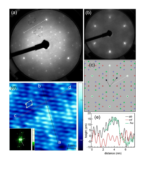
The LEED pattern of 0.9 ML Sn/Au(111) deposited at a substrate temperature () of 413 K in Fig. 1(a) is completely different from the Au(111) substrate in Fig. 1(b). Au(111) exhibits satellite spots around each 11 spot that are related to the 22 reconstruction. On the other hand, the Sn/Au(111) pattern comprises of characteristic pairs of triangles (black dashed) each formed by six spots. These have reflection symmetry across the line (white dashed) joining two adjacent 11 spots. The absence of the satellite spots related to the bare substrate reconstruction obviously means formation of a totally different surface structure. We have simulated the LEED pattern considering a matrixLEEDpat , the three sets of red, green and blue colored spots correspond to three 120∘ rotated domains (Fig. 1(c)). We henceforth denote this structure by (2113). The reciprocal unit cell vectors for one of the domains and the substrate are shown in Fig. 1(c). If (=) is the substrate direct lattice vector, the overlayer direct lattice vectors shown by white arrows in Fig. 2(d) are = , while = . () is rotated by 30∘ (100.9∘) with respect to and thus the unit cell of the overlayer is oblique with = 70.9∘.
A high resolution atomic scale STM image in Fig. 1(d) shows the oblique mesh, where the lengths of the unit cell vectors and are estimated to be 8.40.3 Å and 5.50.3 Å, respectively, which are in the ratio of . The oblique symmetry of the unit cell is also evident with having similar value as obtained from LEED (703∘). The height profiles in Fig.1(e) show that the overlayer is flat with atomic corrugation of 5 pm that is similar to the bare substrate. In contrast to the height profile along cd, the height profile along ab that is perpendicular to cd shows a broad undulation. This is very similar to that observed across the discommensurate lines of the Au(111) herringbone reconstruction (green line in Fig. 1(e)) indicating that although there is no buckling as in stanene, a long range undulation of the Au(111) surface is present. An important conclusion from our LEED and STM studies is that Sn deposition on Au(111) at 413 K does not result in a honeycomb structure.
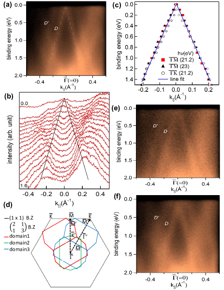
In spite of not being stanene with honeycomb structure, the ARPES of the (2113) phase demonstrates an unexpected result: two branches of highly linear bands () forming a ’’ shape, as shown by white dashed lines in Fig. 2(a)). The bands are linear along - over a binding energy () range starting from 1.5 eV at = 0.2Å-1 to the Fermi level (), where the two branches of ’’ meet at the point. Its linearity is established from the momentum distribution curves (MDC) (Fig.2(b)) from which as a function of (red squares) is obtained (Fig.2(c)).
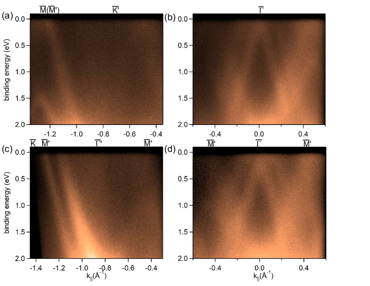
The first Brillouin zone of the (2113) phase obtained from the unit cell determined above is overlaid on that of the substrate in Fig. 2(d). ARPES measured up to the point of the substrate BZ spans the and points of the overlayer BZ when all the domains are considered, but no other linear band is observed at either or (see Fig. S1(a,b) of Supplementary material (SM)supplement ). Similarly, ARPES spectra up to the point of substrate BZ spans the and points of overlayer BZ, but no other linear bands are observed (see Fig. S1(c,d)supplement ). The linear band is observed only at the common zone center of the three domains. The linear bands are not observed at point of domain3 possibly because of overlap with bands related to the other two domains for which this is an arbitrary point and the proximity of intense band of Au.
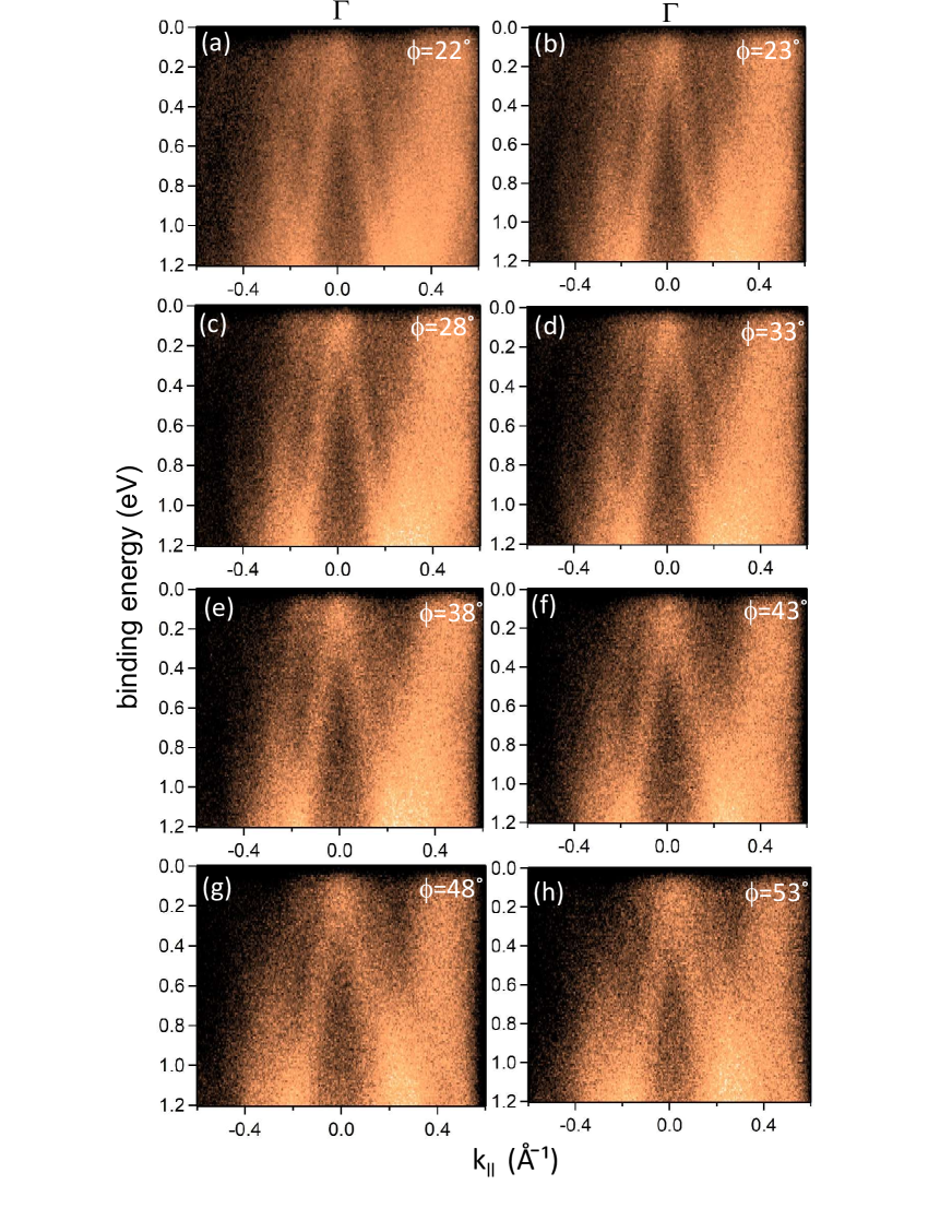
The band is also observed at a different photon energy of 23 eV, the () variation from MDC (solid black triangles in Fig. 2(c)) is very similar to 21.2 eV photon energy showing that it is surface related. Moreover, as expected for a Dirac cone, is unaffected by the variation of the azimuthal angle from the - direction (Fig. 2(a)) to - direction (Fig. 2(f) and black open circles in Fig. 2(c)). The ARPES data for the intermediate azimuthal angles are shown in Fig. S2 of SMsupplement .
A least square fitting obtained from MDC curves of Fig. 2(a,e,f) with a blue straight line provides an excellent fit. The magnitude of the slopes (/) of the left and the right branches are essentially same, 6.880.1 and 6.920.1, respectively. Applying the relation = , the Fermi velocity () turns out to be 1.05106 m/s, which is very similar to that of graphene (1106 m/s)Zhang05 . However, the important differences with graphene is that the structure is non-honeycomb and a single Dirac-like cone is observed at the zone center. Theoretical studies have predicted their existence of such single Dirac cones non-honeycomb structures. For example, the Lieb lattice with a square symmetry hosts a topologically nontrivial invariant insulating phase with a single Dirac cone per BZWeeks10 ; Slot17 . A MoS2 allotrope having square-octagonal ring structure has been shown theoretically to exhibit a single Dirac cone at at the zone center and its is comparable to that of grapheneLi14 . Graphaynes that are rectangular show two nonequivalent distorted Dirac conesMalko12 . We have used a modified Lieb lattice model for our DFT calculations, as discussed latter.
It is interesting to note that another weak linear band in Fig. 2(a,e,f) is observed that is parallel to with a momentum offset of about 0.2 Å-1. Both the branches of cross at 0.2 Å-1. The energy offset between and is about 0.5 eV. It has been shown in an earlier study that Au intercalation in graphene induces large Rasbha spin orbit coupling (soc) of 0.1 eVMarchenko12 . Giant Rashba effect has also been observed in a AuPb binary surface alloy at the surface zone center with a Rashba parameter value of 4.45 eV ÅChen15 . If we interpret to be due to Rashba soc, the Rashba parameter value here is 5 eVÅ, which is similar to AuPb. As in case of , the band is also unaffected by change of photon energy (Fig. 2(e)) and the azimuthal angle (Fig. 2(f) and Fig. S2supplement ).
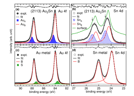
Before proceeding further to understand the origin of the Dirac-like cones discussed above, we have addressed the question of alloying in the (2113) phase. Previous studiesBarthes81 ; Zhang91 using LEED and AES show formation of AuSn surface alloy at RT. Au 4 and Sn 4 core-level spectra of the (2113) phase (Fig. 3(a,b)) are compared with those of the corresponding bulk metals in Fig. 3(c,d). In Fig. 3(c), Au 4 shows the 4 bulk peak at 84 eV, while the surface component (shaded green) is shifted to lower at 83.6 eVCitrin78 . In contrast, for the (2113) phase, the surface component is absent and both the Au 4 spin-orbit split peaks exhibit an asymmetry on the higher side that cannot be accounted for by DS asymmetry. A good quality fit is obtained only when an additional component (, blue shaded) is considered, and its position is varied freely. The main peak () appears at 84 eV, while appears at 0.3 eV higher . position coincides with the bulk component of Au metal (Fig. 3(a,c)) and thus it can be assigned to the underlying substrate. On the other hand, is related to the (2113) 2D surface alloy. This is supported by an earlier work, which show that the Au 4 peak shifts to higher in bulk Au-Sn alloys compared to Au metalFriedman73 .
The Sn 4 spectrum in Fig. 3(d) for Sn metal shows the 4 and 4 peaks at 24 eV and 25 eV, respectively. In contrast, the corresponding peaks in the (2113) phase are both shifted to higher by 0.3 eV. This clearly indicates surface alloying since in bulk Au-Sn alloys, such shift to higher is reported with respect to Sn metalFriedman73 . It is noted that the Sn 4 peaks are broader and fitting with single component fails, indicating presence of at least two components. This is established by the Sn 4 spectrum recorded with higher resolution, where the shoulder depicting the second component is showed by an arrow (Fig. 3(b), green line). Thus, presence of two non-equivalent Sn atom positions in the Au-Sn alloy is indicated. These components ( and ) are separated by 0.3 eV. The composition of the surface alloy is determined to be Au2Sn, considering the areas of and (+ ) and their corresponding photoemission cross-sections. Note that following similar procedure for 0.9 ML Sn deposited on Au(111) at RT, we find the composition to be AuSn, in agreement with literatureBarthes81 . Thus, clearly, besides the surface structure, the composition of the surface alloy also changes with .
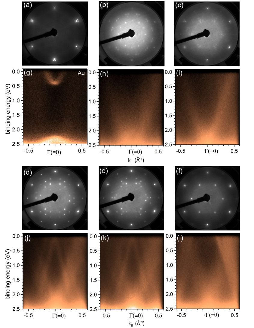
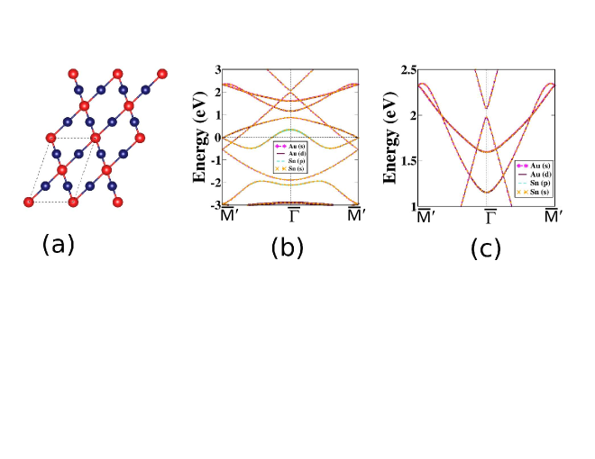
It is important to note that the occurrence of the Dirac-like linear bands in Fig. 2 is specific to the (2113) phase with composition of Au2Sn. The ARPES for the other phases with different surface structure and composition studied by us do not show the linear bands (Fig. S3)supplement . DFT has been extensively used to understand the electronic structure of the 2D materials. However, in order to perform DFT, a starting structural model for the (2113) phase is required. Although we have determined the unit cell, the task of obtaining the atomic positions is complicated due to surface alloying and is outside the scope of the present work. If bare Au(111) surface is considered, the unit cell would comprise of 5 Au atoms in the regular fcc positions with the lattice parameters = 4.89Å, = 7.61Å and = 70.9∘. But, for Au2Sn, a 2:1 ratio of the Au and Sn atoms is not satisfied with 5 atoms in the unit cell. So, we have considered an extra Sn atom noting that the size of the unit cell (= 8.40.3 Å obtained from STM) is larger than the unrelaxed bulk terminated unit cell with = 7.61Å. Among a few structures we have probed, we present here an atomic arrangement following the Lieb lattice that has been shown to host a topologically non-trivial phase with a single Dirac point per unit cell along with a dispersionless band through itWeeks10 . However, in order to be consistent with experiment, we take a non-primitive Lieb lattice with 6 atoms per unit cell and modified to be oblique with = 70.9∘ rather than being rectangularWeeks10 . To retain the inversion symmetry, we assume two Sn atoms to be at the center and corner positions, while the four Au atoms occupy intermediate positions forming a parallelogram with subtended angle of (Fig. S4(a))supplement . The calculated band structures reveal that only for this model, a pair of linear bands meet at the point, but at about 2 eV above and shows a small gap of 130 meV (Fig. S4(b,c)supplement ). These bands originate primarily from the Sn states with some admixture of Au states. However, our experimental data show that the linear bands meet at and also the two shallow parabolic bands crossing the linear bands are not observed (Fig. 2). The reasons for such qualitative disagreement with ARPES could be related to the fact that the (2113) phase occurs only at high temperature and thus it could be a metastable phase, while DFT calculates the lowest energy ground state at zero temperature. Most importantly, we have used only a notional model structure consistent with the experimentally determined unit cell. The disagreement may also be attributed to that. We believe that the complete structure of the (2113) phase needs to be determined experimentally and used as input to the DFT calculation for realistic determination of its electronic band structure.
To conclude, we have identified Dirac-like linear bands at the zone center in Au2Sn surface alloy that has an oblique unit cell described by . This is thus an example of Dirac cone in a non-honeycomb surface alloy. The linear bands forming the Dirac cone have Fermi velocity comparable to that of graphene. It is surprising that exotic electronic structure is possible even in complicated surface alloys. The present results will rejuvenate the search for 2D quantum materials that are important for high speed electronic devices.
D.P. and A.C. thanks P.A. Naik, A. Banerjee for support and encouragement and the Computer Centre of RRCAT, Indore for providing the computational facility.
References
- (1) K. S. Novoselov, A. K. Geim, S. V. Morozov, D. Jiang, M. I. Katsnelson, I. V. Grigorieva, S. V. Dubonos, A. A. Firsov, Nature, 438, 197 (2005).
- (2) A. K. Geim and K. S. Novoselov, Nature Mater. 6, 183 (2007).
- (3) Y. Xu, B. Yan, H.-J. Zhang, J. Wang, G. Xu, P. Tang, W. Duan, S.-C. Zhang, Phys. Rev. Lett. 111, 136804 (2013).
- (4) P. Vogt, P. De Padova, C. Quaresima, J. Avila, E. Frantzeskakis, M. C. Asensio, A. Resta, B. Ealet, G. Le Lay, Phys. Rev. Lett. 108, 155501 (2012).
- (5) C. Kamal, A. Chakrabarti M. Ezawa, New J. Phys. 17, 083014 (2015).
- (6) A. J. Mannix, X. F. Zhou, B. Kiraly, J. D. Wood, D. Alducin, B. D. Myers, X. Liu, B. L. Fisher, U. Santiago, J. R. Guest, M. J. Yacaman, A. Ponce, A. R. Oganov, M. C. Hersam, N. P. Guisinger, Science 350, 1513 (2015).
- (7) L. Li, Y. Yu, G. J. Ye, Q. Ge, X. Ou, H. Wu, D. Feng, X. H. Chen, Y. Zhang, Nature Nanotech. 9, 372 (2014).
- (8) F. Zhu, W. Chen, Y. Xu, C. Gao, D. Guan, C. Liu, D. Qian, S. Zhang, J. Jia, Nature Mater. 14, 1020 (2015).
- (9) C.-Z. Xu, Y.-H. Chan, Y. Chen, P. Chen, X. Wang, C. Dejoie, M.-H. Wong, J. A. Hlevyack, H. Ryu, H.-Y. Kee, N. Tamura, M.-Y. Chou, Z. Hussain, S.-K. Mo, T.-C. Chiang, Phys. Rev. Lett. 118, 146402 (2017).
- (10) J. Deng, B. Xia, X. Ma, H. Chen, H. Shan, X. Zhai, B. Li, A. Zhao, Y. Xu, W. Duan, S.-C. Zhang, B. Wang and J. G. Hou, Nature Mater. 17, 1081 (2018).
- (11) J. Yuhara, Y. Fujii, K. Nishino, N. Isobe, M. Nakatake, L. Xian , A. Rubio and G. L. Lay, 2D Mater. 5, 025002 (2018).
- (12) S. LaShell, B. A. McDougall, E. Jensen, Phys. Rev. Lett. 77, 3419 (1996).
- (13) F. Reinert, G. Nicolay, S. Schmidt, D. Ehm, S. Hfner, Phys. Rev. B 63, 115415 (2001).
- (14) S. Nigam, S. Gupta, D. Banyai, R. Pandey, C. Majumder, Phys. Chem. Chem. Phys. 17, 6705 (2015).
- (15) Y. Guo, F. Pan, M. Ye, Y. Wang, Y. Pan, X. Zhang, J. Li, H. Zhang, J. Lu, 2D Mater. 3, 035020 (2016).
- (16) M. G. Barthes, C. Pariset, Thin Solid Films 77, 305 (1981).
- (17) Y. Zhang, A. J. Slavin, J. Vac. Sci. Technol. A 9, 1784 (1991).
- (18) L. A. Meier, N. J. Castellani, Comp. Mater. Sci. 127, 48 (2017).
- (19) A. Canzian, H.O. Mosca, G. Bozzolo, Surf. Rev . Lett. 17, 391 (2010).
- (20) A. K. Shukla, S. Banik, R. S. Dhaka, C. Biswas, S. R. Barman, Rev. Scientific Instrum. 75, 4467 (2004).
- (21) S. Doniach and M. Šunjić, J. Phys C 3, 287 (1970).
- (22) G. Kresse, J. Furthmüller, Phys. Rev. B, 54, 11169 (1996); G. Kresse, D. Joubert, Phys. Rev. B, 59, 1758 (1999).
- (23) P. E. Blöchl, Phys. Rev. B, 50, 17953 (1994).
- (24) J. P. Perdew, K. Burke, M. Ernzerhof, Phys. Rev. Lett., 77, 3865 (1996).
- (25) LEEDpat, Version 4.2, utility by K.E. Hermann (FHI) and M.A. Van Hove (HKBU), Berlin / Hong Kong, 2014; see also http://www.fhi-berlin.mpg.de/ KHsoftware/ LEEDpat/ index.html.
- (26) Y. Zhang, Y. W. Tan, H. L. Stormer, P. Kim Nature 438, 201 (2005).
- (27) See Supplement material for figures S1 - S4.
- (28) C. Weeks, M. Franz, Phys. Rev. B 82, 085310 (2010).
- (29) M. R. Slot, T. S. Gardenier, P. H. Jacobse, G. C.P. van Miert, S. N. Kempkes, S. J. M. Zevenhuizen, C. M. Smith, D. Vanmaekelbergh, I. Swart, Nature Phys. 13, 672 (2017).
- (30) W. Li, M. Guo, G. Zhang, Y.-W. Zhang, Phys. Rev. B 89, 205402 (2014).
- (31) D. Malko, C. Neiss, F. Vies, A. Grling, Phys. Rev. Lett. 108, 086804 (2012).
- (32) D. Marchenko, A. Varykhalov, M. R. Scholz, G. Bihlmayer, E. I. Rashba, A. Rybkin, A. M. Shikin and O. Rader, Nature Commun. 3, 1232 (2012).
- (33) W.-C. Chen, T.-R. Chang, S.-T. Tsai, S. Yamamoto, J.-M. Kuo, C.-M. Cheng, K.-D. Tsuei, K. Yaji, H. Lin, H-T Jeng, C.-Yu Mou, I. Matsuda, S-J Tang, New J. Phys. 17, 083015 (2015).
- (34) P. H. Citrin, G. K Wertheim, Y. Baer, Phys. Rev. Lett. 41, 1425 (1978).
- (35) R. M. Friedman, J. Hudis, M. L. Perlman, R. E. Watson, Phys. Rev. B 8, 2433 (1973).
Supplementary material for the paper entitled ”Dirac cone in a non-honeycomb surface alloy”
Pampa Sadhukhan1, Dhanshree Pandey2,3, Vipin Kumar Singh1, Shuvam Sarkar1, Abhishek Rai1, Kuntala Bhattacharya4, Aparna Chakrabarti2,3 and Sudipta Roy Barman1
1UGC-DAE Consortium for Scientific Research, Khandwa Road, Indore 452001, Madhya Pradesh, India
2Homi Bhabha National Institute, Training School Complex, Anushakti Nagar, Mumbai 400094, Maharashtra, India
3Theory and Simulations Laboratory, Raja Ramanna Centre for Advanced Technology, Indore 452013, Madhya Pradesh, India
4Department of Physics, Indian Institute of Space Science and Technology, Thiruvananthapuram 695547, Kerala, India
This Supplementary material contains four figures.
