Theoretical Evaluation of Electronic Density-of-states and Transport Effects on Field Emission from -type Ultrananocrystalline Diamond Films
Abstract
In the nitrogen-incorporated ultrananocrystalline diamond ((N)UNCD) films, representing an -type highly conductive two-phase material comprised of diamond grains and -rich graphitic grain boundaries, the current is carried by a high concentration of mobile electrons within the large-volume grain boundary networks. Fabricated in a simple thin-film planar form, (N)UNCD was found to be an efficient field emitter capable of emitting a significant amount of charge starting at the applied electric field as low as a few V/m which makes it a promising material for designing electron sources. Despite the semimetallic conduction, field emission (FE) characteristics of this material demonstrate a strong deviation from the Fowler-Nordheim law in a high-current-density regime when (N)UNCD field emitters switch from a diode-like to resistor-like behavior. Such phenomenon resembles the current-density saturation effect in conventional semiconductors. In the present paper, we adapt the formalism developed for conventional semiconductors to study current-density saturation in (N)UNCD field emitters. We provide a comprehensive theoretical investigation of () the influence of partial penetration of the electric field into the material, () transport effects (such as electric-field-dependent mobility), and () features of a complex density-of-states structure (position and shape of bands, controlling the concentration of charge carriers) on the FE characteristics of (N)UNCD. We show that the formation of the current-density saturation plateau can be explained by the limited supply of electrons within the impurity bands and decreasing electron mobility in high electric field. Theoretical calculations are consistent with experiment.
I Introduction
Field emission (FE) of electrons from the nitrogen-incorporated ultrananocrystalline diamond ((N)UNCD), simply fabricated in a form of thin films, has become a subject of numerous experimental studies. Wu et al. (2000); Corrigan et al. (2002); Ikeda and Teii (2009); Lin et al. (2011); Baryshev et al. (2014) Due to a set of key features defined by the unique diamond/graphite phase nanostructure, these materials can be operated in conditions desirable for efficient electron sources i.e. at low applied electric fields and in a moderate vacuum environment. (N)UNCD field emitters demonstrate a metal-like behavior in the low-current regime. At some critical value of the emission current (and/or critical applied electric field), the behavior of the FE characteristic changes and any further increase of current, due to an applied electric field, occurs at a slower rate which eventually results in a saturation plateau. Such an effect is also observed in other carbon-derived polycrystalline materials with mixed / hybridizationLiao et al. (1998); Xu, Chen, and Deng (2000); Ducati et al. (2002); Varshney et al. (2011); Cahay et al. (2014) and has been speculated to be due to different phenomena, including: electron tunneling through multiple barriers, Liao et al. (1998) an intermediate state between the field emission and thermionic emission regimes, Xu, Chen, and Deng (2000); Ducati et al. (2002) or due to the space-charge effect. Xu, Chen, and Deng (2000); Cahay et al. (2014) Moreover, the observed saturation effect is a long-known characteristic feature of conventional semiconductors Arthur (1965); Baskin, L’vov, and Fursey (1971); Serbun et al. (2013) which has been explored theoretically. Stratton (1955, 1962); Baskin, L’vov, and Fursey (1971)
The original theory describing electron FE from flat metal surfaces by electron tunnelling through a simple triangular potential barrier was developed by Fowler and NordheimFowler and Nordheim (1928) in 1928 and shortly after reconsidered by NordheimNordheim (1928) for Schottky’s image-rounded triangular barrier, and was extended by Murphy and GoodMurphy and Good Jr (1956) in 1956. StrattonStratton (1955, 1962) later adapted the theory to explain FE from semiconductors assuming a spatially constant Fermi level (zero-current approximation). Baskin et al. Baskin, L’vov, and Fursey (1971) reconsidered Stratton’s equations and combined the surface tunneling theory with the bulk parameters of the material obtained from a self-consistent solution of Poisson’s and Ohm’s equations. They showed that both -type and -type semiconductors have a region on a current-voltage characteristic where they deviate from the Fowler-Nordheim (FN) law and linked this behavior to the partial penetration of the electric field into the semiconductor. This effect results in the change of carrier concentration in the near-surface region (creation of the inversion or accumulation layer underneath the surface in a -type and -type semiconductor, respectively) also called the space-charge region. Moreover, they emphasized the significant influence of the field-dependent carrier mobility on the FE characteristics. In Refs. Huang, Qin, and Zhang, 1997; Liu, Chiang, and Heritage, 2006, this approach was used to explain the behavior of FE characteristics from Si field emitters.
For conventional semiconductors, the surface space-charge layer, which arises in a material due to the change in electrostatic potential between the bulk and the surface, has been studied in depth.Kingston and Neustadter (1955); Seiwatz and Green (1958); Stratton (1962); Baskin, L’vov, and Fursey (1971); Huang, Qin, and Zhang (1997); Lin and Liou (1998) In the energy-band diagram, this effect is modeled as a variation of the position of the CB edge with respect to the Fermi level near the surface of the material. (N)UNCD films and other carbon-derived materials have a unique density-of-states structure represented by a combination of and bands associated with - and -hybridized carbon, respectively, present in the fundamental band gap of diamond.Robertson and O’Reilly (1987); Zapol et al. (2001) When exposed to strong electric fields, the downward band bending may cause the formation of a space-charge layer near the surface of -type (N)UNCD. The carrier concentration and the carrier accumulation rate will be defined by the density-of-states structure and the shape of bands, in particular. Literature review suggests that the effect of the density of states on the FE characteristics of (N)UNCD has not yet been explored.
It should be mentioned that the theories behind FE relate the electric field applied to a material and the current density, but not the experimentally measured emission current. Therefore, current density is a crucial characteristic required to be known in order to compare experimental measurements to theoretical predictions and to enable proper comparison of FE properties of different cathodes. UNCD-based electron sources belong to a class of large-area field emitters.Forbes (2009) When assembled in a parallel-plate configuration, the current density is conventionally evaluated as an experimentally measured current normalized by the total area of the cathode or anode (by the smallest of the two areas) which remains constant during all measurements. It was observed Xu, Tzeng, and Latham (1993, 1994); Zhu, Kochanski, and Jin (1998) that in polycrystalline diamond films the electron FE originates from the discrete spots randomly distributed over the surface of the cathode. Recently, we have quantitatively shown Chubenko et al. (2017a) that the surface density of emission sites in (N)UNCD films strongly depends on the magnitude of the applied electric field. It means that the emission area, which contributes to the current density, varies with the electric field as well. The methodologyChubenko et al. (2017a) developed for determining the FE area from large-area electron emitters makes it possible to study the current-density saturation effect present in -type (N)UNCD films and to confirm or reject various hypotheses, which were proposed in the past, on the nature of this effect.
The purpose of the present work is to adapt the formalism developed for conventional semiconductors in order to explain the current-density saturation effect in -type polycrystalline-diamond-based electron sources which have a characteristic density-of-states structure. In particular, we show how the FE characteristics of (N)UNCD depend on () the position of the Fermi level at the surface of the material, () the shape and magnitude of the density of states, and () the field-dependent mobility.
The paper is organized as follows. In Section II, we briefly review the Stratton-Baskin-Lvov-Fursey formalism, describing the processes and effects in the bulk and at the surface of a semiconductor exposed to a high applied electric field. In Section III, we adapt the approach described in Section II to calculate the current-voltage characteristics of (N)UNCD films. In Section IV we compare theoretical results to experimental measurements. For convenience, we provide a brief summary of our recent findings Chubenko et al. (2017a, b, c) on the field-dependent FE area of (N)UNCD films. We discuss the formation of experimentally estimated current-density saturation limits and the difficulties associated with evaluation of the FE area from planar polycrystalline diamond materials. Conclusions and outlooks are summarized in Section V.
II Current-Density Saturation in Conventional Semiconductors
II.1 Semiconductor in Applied Electric Field

We consider a one-dimensional modelBaskin, L’vov, and Fursey (1971) of a uniformly-doped semi-infinite semiconductor, i.e. the influence of a substrate on the FE process is neglected. When the voltage is applied between a semiconducting field emitter and an anode, the resulting electric field penetrates into the semiconductor and causes the bending of valence and conduction bands. For example, in -type semiconductors a narrow accumulation layer appears at the surface of a field emitter (see Fig. 1), giving rise to the concentration of free electrons in the CB. Therefore, the FE current density in a low-field regime is limited by the tunnelling probability of CB electrons in the near-surface region through the field-deformed potential barrier and thus demonstrates a metal-like behavior.Baskin, L’vov, and Fursey (1971); Liu, Chiang, and Heritage (2006)
As the applied electric field increases and penetrates deeper into the interior, the FE current density becomes limited by the supply of electrons. Moreover, scattering mechanisms that involve optical phonons become significant, limiting the hot-carrier mobility at high electric fields.Baskin, L’vov, and Fursey (1971) This is the saturation regime.
Definition of all energies used in the calculations is given in Fig. 1, where we use an energy diagram of an -type semiconductor as an example. and are the conduction band minimum (CBM) and the valence band maximum (VBM), respectively. and are the Fermi level and the donor level (for -type semiconductor, the acceptor level placed close to the VBM is used instead), respectively. is the energy of a donor level with respect to the CBM and is the band-gap energy. and are the functions characterizing the position of the CBM and the Fermi level within the material, respectively, with respect to the vacuum level . and are the electron affinity and the work function, respectively. Function defines the position of a CBM with respect to the Fermi level and thus determines the carrier concentration at any point in the material. The subscript will be used to distinguish between the values measured at the surface (i.e. at ) and those measured in the interior.
II.2 Poisson’s Equation
To describe the space-charge, or the band-bending, region in a conventional semiconductor, an approach similar to the one described in Ref. Baskin, L’vov, and Fursey, 1971 can be used. In Poisson’s equation,
| (1) |
the potential difference is related to the potential energy as
| (2) |
where , the electron charge, allows for converting between V to eV. is the dielectric constant of a semiconductor and is the permittivity of free space. The charge density in the semiconductor bulk is given by (see, for example, Ref. Li, 2006)
| (3) |
Here the volume densities of electrons , holes , negative acceptor ions , and positive donor ions are defined as
| (4) |
where is the effective density of states in the CB and is the effective density of states in the VB. Here, and are the density-of-states effective mass of electrons and holes, respectively, is Boltzmann’s constant, is the lattice temperature, and is Planck’s constant. is the Fermi-Dirac integral of the order . and are the concentrations of acceptor and donor atoms, respectively.
It is convenient to introduce a dimensionless variable
| (5) |
In terms of , Eqs. 4 can be rewritten as
| (6) |
The resulting equation to solve is
| (7) |
The relation between the spatial coordinate and the variable can be obtained by the Ohm’s law,
| (8) |
where is the current density, and and denote the electron and hole mobilities, respectively. The low-field carrier mobility in semiconductors depends on the temperature and on the doping density, . The doping-dependence of both majority-Masetti, Severi, and Solmi (1983); Reggiani et al. (2002) and minority-carrier mobilityCaughey and Thomas (1967); Reggiani et al. (2002); Swirhun, Del Alamo, and Swanson (1986); Swirhun, Kwark, and Swanson (1986) at room temperature are described by the empirical expression
| (9) |
where , , , , , , and are the parameters obtained by fitting experimental data (e.g., see data for Si in Ref. Masetti, Severi, and Solmi, 1983 ).
Moreover, it was revealed experimentallyRyder (1953); Gunn (1956); Prior (1959); Schweitzer and Seeger (1965) that the mobility of electrons and holes in semiconductors become field-dependent when the internal electric field reaches its critical value . Thus, the linear relation between the current density and the electric field , (or between the drift velocity and the electric field , ), fails at . The theoretical interpretation of this phenomenonShockley (1951) is that the carrier mobility in semiconductors is limited by the scattering by acoustic phonons at weak fields ( V cm-1) and by the scattering by optical phonons at larger fields ( V cm-1). In the first case, the mobility remains constant with the electric field, and in the second case, it decreases according to the parametric expressionCaughey and Thomas (1967)
| (10) |
where for holes and for electrons. Note that in this section we use to denote the internal electric field. and will be used below to denote the surface electric field in vacuum and the applied electric field, respectively.
Using the relation between the internal electric field and the electrostatic potential ,
| (11) |
and Eq. 5, Eq. 8 can be rewritten as
| (12) |
Finally, we obtain
| (13) |
With Eq. 11 and Eq. 13, Poisson’s equation 7 becomesBaskin, L’vov, and Fursey (1971)
| (14) |
This differential equation can be solved numerically for a fixed using the boundary condition
| (15) |
where can be found from Ohm’s law in the bulk,
| (16) |
Here corresponds to the position of the Fermi level in the bulk material and can be obtained from the charge neutrality condition in thermal equilibrium which is mathematically expressed as .
II.3 Stratton’s Equations
In the simplified form, Stratton’s equationsStratton (1962) for the electron current densities and emitted from the semiconductor surfaces with negative () and positive () Fermi energies, respectively, under the electric field at the surface can be written as
| (17) |
where , , and . Numerically, A cm-2 for K, V eV-3/2cm-1, and eV-1/2cm-1. is measured in eV and in V cm-1. and are special elliptic functions (known as Nordheim functions) of the argument , where eV cm1/2 V-1/2.
| (18) |
where A eV V-2 and V eV-1/2 cm-1. . We use an approximate expression for the Nordheim function, , given by Forbes (2006)
| (19) |
and assume that .
II.4 Combined Poisson’s and Stratton’s Equations
Self-consistent graphical solutions of Poisson’s and Stratton’s equations give the value of for each specified.Baskin, L’vov, and Fursey (1971) Poisson’s equation provides the solution for the internal electric field , i.e. at the interior boundary of the material/vacuum interface, whereas the Stratton’s equations give the solution for the local electric field realized at the emitting surface outside in vacuum, such that . All vs. curves shown in this work were obtained by this method. The local electric field at the surface is related to the magnitude of the applied electric field through the enhancement factor as
| (20) |
Eventually, vs. curves can be calculated and compared to the experimental results using as an adjustable parameter.
III Electronic Density-of-States and Transport Effects on Field Emission from (N)UNCD Films
III.1 Subtleties of Electron Conduction in (N)UNCD Films
It has been shown both theoretically by the tight-binding simulations Zapol et al. (2001) and experimentally by the scanning tunneling-field emission microscopy Karabutov et al. (1999); Harniman et al. (2015) that the electron field emission in (N)UNCD films originates from the grain boundaries rather than from sharp grains. It was also shownZapol et al. (2001); Corrigan et al. (2002) that the electronic properties of (N)UNCD films are controlled by the -bonded carbon atoms present in the grain boundaries of the material. A graphitic phase places impurity bands ( bands) inside the fundamental diamond band gap ( bands) that effectively reduces the optical band gap of polycrystalline diamonds. The addition of nitrogen during the growing process increases the density of states in bands,Zapol et al. (2001); Chen et al. (2001) causes delocalization of electron states,Beloborodov et al. (2006); Achatz et al. (2006a) and leads to an increase in both the grain size and grain-boundary width,Bhattacharyya et al. (2001); Birrell et al. (2002) giving rise to a number of unique properties. For instance, compared to the nearly insulating UNCD, (N)UNCD becomes a highly conductive material with the current being carried by a high concentration of highly mobile electrons within the large-volume grain boundary networks. Experimental measurements Bhattacharyya et al. (2001); Williams et al. (2004); Achatz et al. (2006a); Ikeda et al. (2008) show that the conductivity is of -type. With increasing nitrogen content, the conductivity in (N)UNCD becomes insensitive to temperature,Bhattacharyya et al. (2001); Achatz et al. (2006a) showing a quasimetallic behavior.Achatz et al. (2006a) Conduction was explained to be due to the existence of delocalized interband-gap defect bands. This is different from low-conductive (N)UNCD films, in which electron transport was found to occur via a variable range hopping mechanism across localized states near the Fermi level.Achatz et al. (2006a); Beloborodov et al. (2006)
(N)UNCD films are characterized by a high value of the field enhancement factor , typically several hundred. The mechanism of the field enhancement in (N)UNCD films and other materials with mixed bonding is commonly attributedIlie et al. (2000); Carey, Forrest, and Silva (2001) to the dielectric inhomogeneities within the film originating from the difference between conductive spatially-localized -rich clusters surrounded by a more insulating matrix. The field lines focus onto the localized conductive grain boundaries, providing large local electric fields and locally decreasing material work function.Ilie et al. (2000) Therefore, the enhancement is determined by the geometry of grain boundaries and/or the presence of a space-charge region. Ilie et al. (2000)

III.2 Density-of-States Model
The energy-band structure of (N)UNCD films and other -rich polycrystalline materials is conventionally modeled Robertson and O’Reilly (1987) as a combination of and bands associated with and carbon, respectively, present in the band gap of diamond. It was shown Dasgupta et al. (1991); Nesládek et al. (1996); Zammit et al. (1998) that the density of states in the bands can be approximated by Gaussian functions centered at and and described by the variance (see Fig. 2). The extended bands and band tails can be represented by the square-root functions and the exponential functions decaying into the band-gap region, respectively. Assuming that the and , and , as well as and bands are symmetric about the diamond midgap energy, Robertson and O’Reilly (1987) the expressions for densities of states can be written as
| (21) |
Here all energies are measured with respect to the valence band maximum of diamond. is the magnitude of Gaussian functions at . , where is the energy separation between the extended states (fundamental band gap), and is the energy separation between the localized states (pseudo band gap) as shown in Fig. 2. Constant as well as , (the energy at which merges with ), (the energy that determines the slope of band tail decay), and are the fitting parameters that can be extracted from experimental absorption spectra.
Optical transitions under the photoexcitation with the energy are described by the absorption coefficient that is given at K as Tauc (1974); Yu and Cardona (2010)
| (22) |
where are the densities of the initial and final states. The constant is given by
| (23) |
where is the reduced Planck’s constant, is the optical matrix element, is the localization length, is the free electron mass, in the speed of light, and is the refractive index of the material. We assume that has the same value as in a crystalline material, i.e. ,Tauc (1974) where AlZahrani and Srivastava (2009) is the lattice constant of graphite. Using physically reasonable values for other parameters (the localization length which is of the order of a grain-boundary width of (N)UNCDBeloborodov et al. (2006) and a refractive index as that of graphitePelton et al. (1998)), can be estimated as eV2cm5. From this, the optical transitions between the and the bands can be written in the following form
| (24) |
where and are often usedNesládek et al. (1996); Zammit et al. (1998); Achatz et al. (2006b) as generalized fitting parameters available in the literature. This allows the density of states, defined in Eq. 21, to be rewritten in terms of coefficient and fitting parameters , , , , , , and .
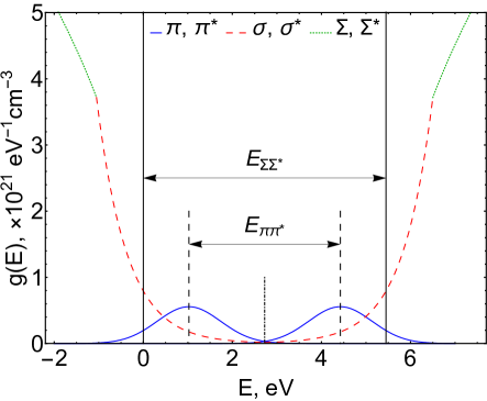
In general, the density-of-states parameters depend on many aspects, including the concentration of nitrogen, conditions of material growth, and so on. In Table 1, we summarize the parameters for density-of-states model for several carbon-derived materials (synthetic diamond films, amorphous carbon films etc. synthesized by chemical or physical vapor deposition (CVD or PVD) methods) available in the literature. The exemplary density-of-state curves for a polycrystalline diamond film calculated using the fitting parameters taken from Ref. Zammit et al., 1998 for one particular sample labeled 860-20 are shown in Fig. 3. For this purpose, we use the localization length comparable with a grain-boundary width of undoped nanocrystalline diamond films.Csencsits et al. (1996) As discussed in Ref. Bhattacharyya and Silva, 2005, the overlapping of interband-gap bands leads to the production of electron states at and above the Fermi level. As the amount of -phase in grain boundaries increases, the density of states at the midgap energy rises up, filling the energy gap. For strongly overlapping bands, the conductivity becomes semimetallic.
The effect of nitrogen on the position of the Fermi level in the fundamental band gap has been discussed in the literature.Zapol et al. (2001); Robertson and O’Reilly (1987) Since we rely on the density-of-states model to be symmetric about the fundamental-gap center,Robertson and O’Reilly (1987); Zammit et al. (1998); Achatz et al. (2006b) the charge neutrality condition requires that the Fermi level coincides with the midgap energy. Under this assumption, the midgap density of states and electron concentration are defined by the degree of overlapping between the and bands.
| Polycrystalline diamond filmsZammit et al. (1998) | -C, -C:HDasgupta et al. (1991) | UNCDAchatz et al. (2006b) | (N)UNCDAchatz et al. (2006b) | |
|---|---|---|---|---|
| , eV | 2.5 | 2.1 | ||
| , eV | 0.4 | 0.53 | ||
| , eV | - | - | - | |
| , eV | - | - | - | |
| , cm-1 | - | |||
| , cm-1eV-1/2 | - | - | - |
III.3 Application of Poisson’s and Stratton’s Equations to -rich Diamond Films
Using the results of the previous section, the carrier charge density, which appears in Poisson’s equation (Eq. 14), for the case of -rich polycrystalline materials can be found as
| (25) |
where
| (26) |
and
| (27) |
Introducing the dimensionless variable
| (28) |
the Fermi-Dirac distribution can be written as
| (29) |
Assuming that the Fermi level in the bulk lies in between and peaks, we find .
Substituting the density of states , defined by Eq. 21, and the Fermi-Dirac distribution , defined by Eq. 29, the expressions for the concentrations of electrons in and bands become
| (30) |
The concentrations of holes in and bands can be found as
| (31) |
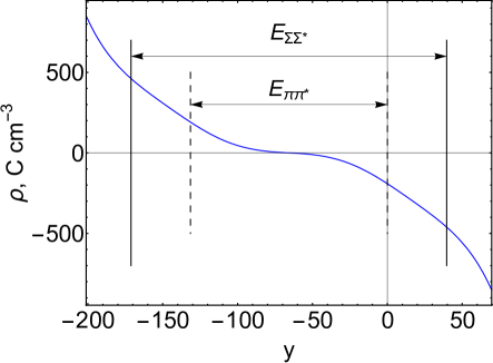
In Fig. 4, we show the calculated vs. curve which assumes the density-of-states structure shown in Fig. 3. The increase and broadening of and bands lead to the increasing charge density in the diamond band gap.
As mentioned above, it is rigorously established that the bulk electrical conduction properties of (N)UNCD films are determined by the carbon represented by the and bands. Below, we show how the shape of these bands, their position in the fundamental diamond band gap, and the decrease of carrier mobility in strong electric fields affect field emission properties of -rich polycrystalline materials. For (N)UNCD films, only band density-of-states parameters are available in the literature.Achatz et al. (2006b) To describe bands, we use the parameters , , and typical for polycrystalline diamond films per Ref. Zammit et al., 1998. The choice of these parameters though is not expected to affect the resulting FE characteristics significantly. For simplicity, we do not consider the contribution from the hopping mechanism which may take place due to the presence of localized states.Bhattacharyya and Silva (2005) Investigation of the temperature effects on FE properties of (N)UNCD is beyond the scope of this work.
III.3.1 Effect of Field-Dependent Mobility
| Parameter | Value | Reference |
|---|---|---|
| , eV | 5.45 | Ref. Zammit et al.,1998 |
| , eV | 2.1 | Ref. Achatz et al.,2006b |
| , eV | 0.53 | Ref. Achatz et al.,2006b |
| , eV | 6.5 | Ref. Zammit et al.,1998 |
| , eV | 0.68 | Ref. Zammit et al.,1998 |
| , cm-1 | Ref. Achatz et al.,2006b | |
| , cm-1eV-1/2 | Ref. Zammit et al.,1998 | |
| , cm2V-1s-1 | 1.5 | Ref. Williams et al.,2004 |
| , V cm-1 | 104 | |
| , | 10 | Ref. Beloborodov et al.,2006 |
| 4.5 | Ref. Beloborodov et al.,2006 | |
| , eV | 3.6 | Ref. Pérez Quintero et al.,2014 |
It was noticed Conwell (1967) that the dependence of electron mobility on the applied electric field has similar character for most conventional semiconductors, except that larger fields are required to produce deviations from Ohm’s law (the region of the drift-velocity saturation) in materials with lower electron mobilities. The saturation of the drift velocity in semiconductors originates from the inelastic scatterings of highly energetic electrons on optical phonons. For the case of polycrystalline diamond films and (N)UNCD films, in particular, there is no available data for the dependence of the carrier mobility on the applied electric field. Therefore, we apply a simple expression commonly used for semiconductors Baskin, L’vov, and Fursey (1971); Ryder (1953)
| (32) |
to describe hypothetical field effects on carrier mobility after the electric field reaches a critical value and to evaluate the importance of this effect (if exists) on the resulting current-density curve behavior.
Electron mobilities in typical semiconductors significantly exceed the mobilities of electrons in -rich materials (compare: cm2V-1s-1 ( V cm-1)Ryder (1953); cm2V-1s-1 ( V cm-1)Ryder (1953); cm2V-1s-1 Williams et al. (2004)). Therefore, it can be assumed that the deviation from Ohm’s law in -rich materials may occur at relatively large electric fields V cm-1. The density-of-states model parameters and material parameters, that are used to calculate FE characteristics of (N)UNCD, are summarized in Table 2.
The comparison presented in Fig. 5 reflects the significant effect which the field-dependent mobility may impose onto the electric characteristics of (N)UNCD. Obtained FE characteristics result from the self-consistent solution of Poisson’s equation (Eq. 14, the red curves in the insets) and Stratton’s equation (Eq. 17, the green curves in the insets). The intersections of the two sets of curves (red and green) provide the resulting current-density dependencies on the electric field. Plots in Fig. 5 and Fig. 5 take field-independent and field-dependent mobility into account, respectively. For the set of density-of-states model parameters specified in Table 2, deviation of the current-density curve from the FN law and further saturation occur in both cases, but the remarkable difference exists. If the field-dependence of the mobility is taken into account, a saturation plateau lies at about 105 A cm-2 which is two orders of magnitude lower as compared to the case considering the mobility independent of the electric field and yielding the saturation plateau as high as 107 A cm-2. For , the mobility is still finite. Therefore, the presence of current-density saturation effect is due to the limited surface metallization rate (this rate is obviously higher than for ), in other words, it is due to the limited electron supply into the accumulation region.
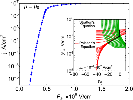
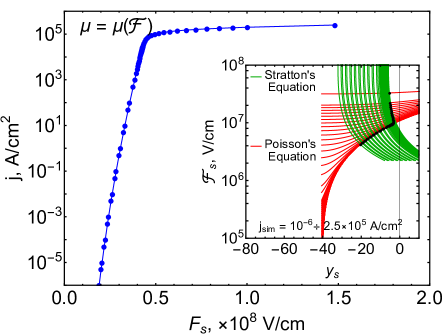
This result emphasizes the importance of field effects on the transport properties in (N)UNCD and encourages further experimental study to help refine (confirm or rule out) existing models on field emission for semiconductors or semimetals, i.e. beyond FN-like formalism. We note that the choice of the mechanism affecting carrier mobility leads to saturation plateaus that may differ by several orders of magnitude. For instance, the current density saturating at 107 A cm-2 is troublesome because it does not allow for distinguishing between the material-driven saturation and the saturation due to Child-Langmuir effect that becomes significant at a current density 107 A cm-2.Dyke and Trolan (1953); Barbour et al. (1953)
III.3.2 Effect of Dielectric Constant
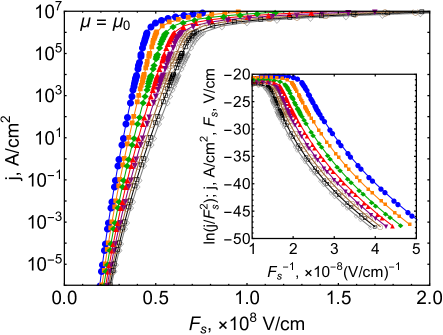
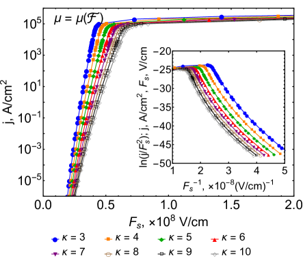
The dielectric constant, , is defined as the ratio between the electric field in vacuum and the electric field in the material, i.e. . Its effect on the FE current density is shown in Fig. 6. We plot the results in semi-log and FN, vs. , coordinates.
Fig. 6 illustrates the effect of on the vs. curve as varies from 3 to 10. The lower the the lower the surface field because field enhancement drops: this result means that as decreases, the electric field line termination at the surface weakens (stronger field penetration into material) and local electric field decreases. At the same time, as expected, does not have any appreciable affect on the saturation plateau. Another interesting result seen in Figs. 6 and 6 is that the field-dependent mobility leads to faster switching from the FN to saturation regime due to a limited charge transport time in the bulk (drift velocity gets saturated). Dielectric constant is commonly used to describe (N)UNCD and other polycrystalline carbon materials. Beloborodov et al. (2006) We use the average value in all calculations below.
III.3.3 Effect of Density of States
It was experimentally shown Achatz et al. (2006b) that the incorporation of nitrogen, the source of high electric conductivity, leads to reduced separation between the peaks ( parameter, pseudo band gap, decreases) and broadening of the peaks (increase of the parameter). Simultaneously, the normalization parameter increases. In Figs. 7–9, we show how variation of these parameters modifies the resulting FE characteristics of (N)UNCD. In order to pinpoint the effect imposed by , , and , we calculate the vs. profiles by sweeping or or while keeping all remaining parameters fixed at the values specified in Table 2.
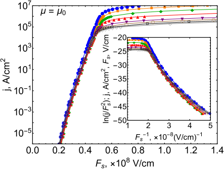
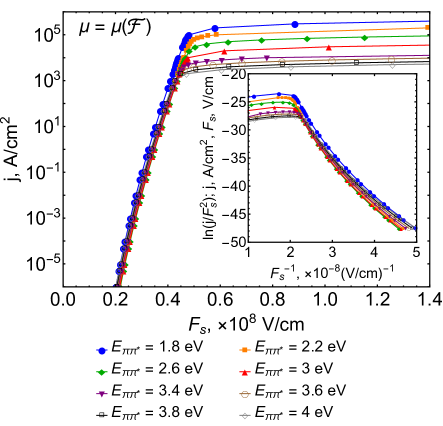
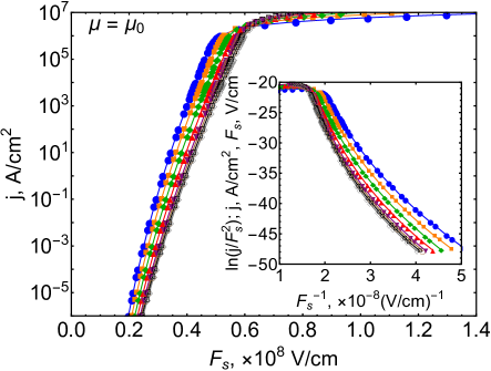
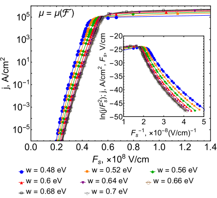
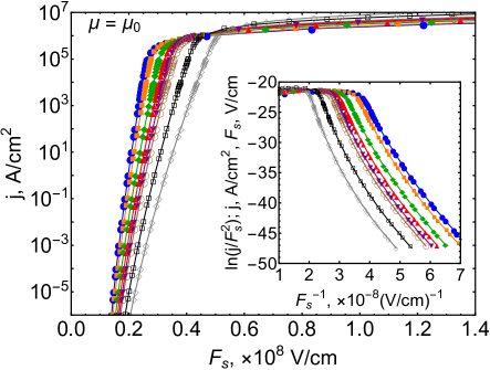
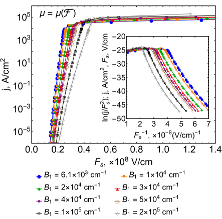
It can be seen in Fig. 7 that variation of parameter does not have significant effect on the FN part of the current-density curve. At the same time, one can see that higher current densities can be obtained from the samples characterized by narrower pseudo band gaps thanks to larger electron supply. The same supply argument exists behind the observed saturation plateau scaling – the smaller the pseudo band gap the larger the electron supply, the larger the saturation plateau.
The increase in (Fig. 8) and (Fig. 9) implies that the electron concentration increases which is equivalent to the increase in conductivity. This leads to a significant shift of the FN-like part toward higher surface fields, which means that a higher electron concentration leads to stronger focusing of electric field lines on more conductive grain boundaries, providing higher field enhancement factor . This result correctly predicts the trend, often observed in experiment, in that UNCD films with higher nitrogen content (i.e. higher conductivity) demonstrate lower turn-on electric fields. At the same time, the effect of and on the saturation plateau for the given pseudo band gap of 2.1 eV, while significant (about 10-fold effect), is not as strong as when is varied (about 100-fold effect). From extended modelling (not shown here) we additionally conclude that the effects of and on the FE properties (including the saturation plateau) should become stronger as further reduces below 2.1 eV. Thus, with increasing parameters and we predict to observe stronger influence on a FN part of the vs. dependence by means of increasing the local field enhancement and lowering the turn-on field. The parameter is primarily responsible for current density saturation – this is because defines the depth of accumulation well near the surface/vacuum interface and therefore defines how fast it depletes.
As seen previously, in all cases field-independent mobility model formulation leads to overall larger saturation plateaus compared to those obtained by taking field-dependent mobility.
IV Comparison to Experiment and Discussion
IV.1 Experimental Results
A detailed description of the methods and techniques used to evaluate the plan-view area of electron emission can be found in Ref. Chubenko et al., 2017a. Here, we present a brief overview of the main ideas and provide crucial findings for the (N)UNCD/Ni/Mo/SS1 sample tested at the cathode-anode separation of 106 m (the (N)UNCD film was grown as described elsewhere Pérez Quintero et al. (2014); Baryshev et al. (2014) on top of a 4.4 mm diameter stainless steel (SS) stub with a Ni/Mo buffer layer).
To visualize electron FE patterns, the YAG:CE/Mo (yttrium aluminum garnet crystal doped with cerium and coated with molybdenum) anode screen was used as an electron-collecting electrode. Green light is emitted when electrons hit the anode. This effect, which is known as cathodoluminescence, allows for mapping of FE patterns on the anode surface. The photocamera viewing the back side of the anode was used to collect the FE images, and current-voltage measurements were done concurrently. To estimate the area of FE patterns formed on the YAG screen, an image-processing algorithm was developed. A comprehensive description of the procedure and the implementation details are provided in the Supporting Information Section of our previous paper.Chubenko et al. (2017a) After the numerical processing of a full dataset of electron emission micrographs, it was found that the FE area strongly depends on the applied electric field through the continuously increasing number of FE sites and through the expansion of FE spots with an increasing electric field.
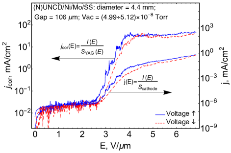
The maximal FE current measured from this particular sample was about 100 A at 6.8 V m-1. The corresponding maximal current density estimated by the conventional method, i.e. by normalizing the experimentally measured current over the entire cathode area = constant,
| (33) |
was found to be 1 mA cm-2 as shown in Fig. 10. This latter method appears to be unreliable to describe fundamental emissive properties of nanodiamond films since it does not account for the increase of the current due to the increase of the number of emission sites which, as described above, is a characteristic feature of (N)UNCD field emitters. Therefore, it leads to a wrong interpretation of experimental results when compared to theory.
The apparent underestimation of the field emission current density due to the overestimation of the actual field emission area can be reduced if the experimentally measured current is normalized by the dynamic FE area defined as the total area of the FE sites formed on the YAG screen and estimated by the algorithmChubenko et al. (2017a)
| (34) |
This new method leads to a quantitatively and qualitatively different behavior compared to that obtained by the conventional method. In a semi- plot (see Fig. 10), rises linearly in a low-current-density region, demonstrating Fowler-Nordheim-like behavior, and saturates at about mA cm-2 starting from V m-1, further demonstrating a plateau.
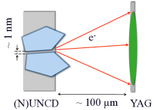
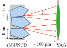
From this we concludedChubenko et al. (2017a) that the current-density saturation level of mA cm-2 represents a basic intrinsic property of (N)UNCD materials. However, the normalization factor may still be unrealistic. In order to estimate the true FE current density, i.e. the current density obtained by normalizing the measured FE current by the cathode surface area from which the current was collected, additional corrections due to electron trajectories and/or fraction of emitting grain boundaries should be taken into account.tha For this purpose, the following approximations can be made. If we assume that every single spot on the screen is formed by electron emission from a single grain boundary representing a square of approximate area 1 nm 1 nmiiiNitrogen incorporation results in a morphology change: the average grain size increases from about 4 to 16 nm and the grain-boundary width increases from about 0.5 to 2.2 nm as the nitrogen content in plasma is changed from 0 to 20.Birrell et al. (2002) In the calculations, we use an average grain size 10 nm and the grain-boundary width 1 nm. as shown in Fig. 11, then the current density can be estimated as
| (35) |
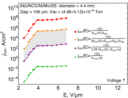
where the number of local maxima, , is defined as a number of emission sites estimated by our algorithm and cm2. Under this assumption, the current density is obviously overestimated (see the upper curve in Fig. 12), since it was experimentally shown Xu, Tzeng, and Latham (1994) that a single FE spot on an anode is formed by several sub-emission sites originating from grain boundaries surrounding diamond grains (see the schematic in Fig. 11). If we assume that the average radius of grains is about nm and the average width of grain boundaries is nm, the average area of a grain and the area of a surrounding grain boundary can be estimated as and , respectively. Then the surface fraction of grain boundaries can be simply found as . Moreover, if we assume that in (N)UNCD films only 52 of grain boundaries are -bonded, as was estimated in Ref. Corrigan et al., 2002, we obtain a correction coefficient . It should be noticed that, at high values of the applied electric field, some optical effects (e.g., blooming and/or other YAG screen post-glowing effects) may arise and lead to overestimation of the emission area. Nevertheless, our algorithm can identify the number of emission sites with high accuracy. Therefore, we use the product of the average area of the emission sites detected on low-current micrographs ( cm2), when the glowing effects are minimal, and the number of LM found on each micrograph (rather than the total found area ). The current density can then be estimated as
| (36) |
As mentioned earlier, the electric-field lines focus onto the localized conductive (N)UNCD grain boundaries, providing large local electric fields, but also modifying electron trajectories. The latter causes the emitter-size change as compared to that seen on the YAG screen. In a simple approximation of straight-line trajectories, the correction due to this effect is given by the field enhancement factor . The current density then becomes
| (37) |
The resulting curve is shown in Fig. 12.
Under these assumptions, the local FE area still could be overestimated since all surrounding grain boundaries are allowed to participate in electron emission. It was found from the mean transverse energy measurements Chen et al. that 1 kV electrons are emitted from the (N)UNCD films at the angle to the surface normal. If we assume that a grain boundary is a point electron emitter (see Fig. 13), then the FE area formed on an anode screen placed at a distance m from such emitter is cm2. The minimal number of emitters required to form an estimated FE area on a YAG screen can be found from the ratio . Then the upper limit of the current density can be estimated by normalizing the current by this ratio and the approximate area of a grain boundary
| (38) |
The resulting curve is shown in Fig. 12.
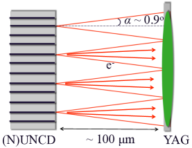
After all approximations are taken into account, we find the experimental current density lies within the shaded limits shown in Fig. 12, i.e. somewhere between and A cm-2. This result is in agreement with Ref. Zhu, Kochanski, and Jin, 1998, where the experimental local current density of nanostructured diamond films was estimated to be more than A cm-2. A more accurate evaluation of the experimental current density requires a detailed simulation of the electron trajectories from UNCD surface in an electric field. However, the main difficulty in the estimation of the FE area comes from the inability to determine the fraction of emitting GBs which form an isolated emission spot on the YAG screen.
IV.2 Correlation between Theory and Experiment
| , eV-1cm-3 | |||||
|---|---|---|---|---|---|
| , eV-1cm-3 | |||||
| , cm-3 | |||||
| , cm-3 | |||||
| , A cm-2 | |||||
| , A cm-2 |
To calculate FE characteristics of highly conductive (N)UNCD films and compare against the obtained experimental results, we use the parameters listed in Table 2. In the literature,Nesládek et al. (1996); Zammit et al. (1998); Achatz et al. (2006b) describing subgap absorption in polycrystalline carbonic materials, coefficients and are used as general fitting parameters. However, to estimate the carrier concentrations, needs to be included in Eqs. 30 and 31 explicitly. contains information about the localization length, (see Eq. 23), which increases with increasing delocalization of the defect states. We use the localization length as a free model parameter since its value is not known from experiment. The enhancement factor is used as an adjustable parameter when the theoretical curves, vs. , are compared to the experimental results, vs. , represented by the uncertainty gray-shaded range in Fig. 12. Numerical results for some electronic and FE characteristics calculated as a function of the localization length are summarized in Table 3.
Results for the field-independent mobility are shown in Fig. 14. For , the current-density saturation plateau reaches up to about A cm-2, a few orders of magnitude outside the experimental upper saturation limit. For the localization length , indicating strong delocalization of the interband-gap states, the calculated saturation plateau overlaps with the experimental upper limit. Overall, it is found that our model overestimates the experimental current-density plateau in the regime of constant mobility.
When the dependence of the electron mobility on the applied electric field is taken into account, there are substantial differences that occur. The results are shown in Fig. 14. Here, all calculated current-density curves lie within the experimentally determined boundaries, between and A cm-2. This finding emphasizes the importance of knowing exact relations since limited electron transport, as can be seen, is an important factor behind the saturation effect. Generally speaking, carrier mobility can be limited by ionized-impurity, acoustic and/or optical phonon, and electron-electron scattering. In polycrystalline materials like (N)UNCD that have conductivity through grain boundary networks, an additional type of scattering, scattering from a grain/grain boundary interface, could have significant effect. Detailed experimental studies of the electron-mobility response to strong electric fields would be necessary to further refine our calculations.
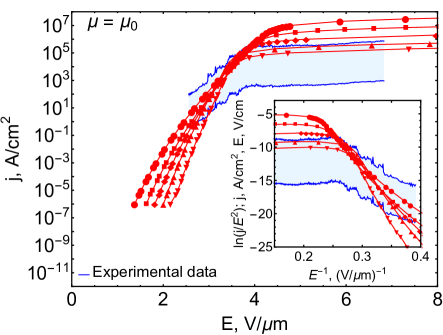
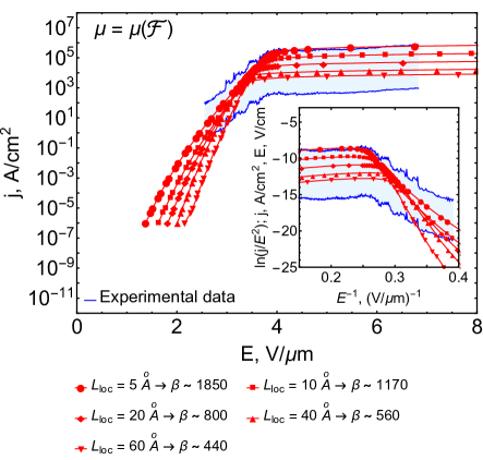
Fig. 14 also demonstrates that the saturation plateau is sensitive to the localization length. According to Eq. 30, . Therefore, an increase in the localization length, with all other parameters unchanged, results in decreasing carrier concentration. This in turn restrains the current density at a lower value. Resulting from our model, the electron concentration in the bulk of the material is about cm-3, depending on the localization length as shown in Table 3. If the band bending, induced by the strong electric field, results in reduced separation between and , such that position of the Fermi level coincides with a maximum of a band (), then carrier concentration near the surface can increase up to cm-3. This will give rise to the emission current in a metal-like manner. At some point, supply of electrons to the near-surface region becomes limited eventually resulting in the saturation behavior.
Comparison to experiment suggests that the correct choice for is between 10 and 40 . This is in line with expectations because matches the average grain-boundary width of highly N-incorporated UNCD, and simultaneously places the calculated current saturation plateau in the middle of the -fork and predicts the field enhancement factor close to the experimentally derived values. Therefore, the provided model fundamentally relates saturation effect and the turn-on field through the electron supply: fast deviation from the FN-like dependence and current-density saturation at moderate values is a signature of the limited electron supply that is a second important factor behind the saturation effect.
Based on the obtained insights, we conclude that FE characteristics of a large-area planar field emitter, such as (N)UNCD, suffer from intrinsic electronic properties rather than from screening the electric field due to high critical emitted current densities A cm-2.Dyke and Trolan (1953); Barbour et al. (1953) Therefore, the Child-Langmuir law, a leading explanation for the saturation effect so far,Cahay et al. (2014) cannot account for the FE current-density saturation in (N)UNCD. Further detailed understanding of saturation in (N)UNCD will require more information on the band structure and transport via optical and high field transport experiments carried on samples with well controlled doping. Emission-area-resolved field emission experiments should be also further improved in terms of accuracy and precision to enable more reliable vs. dependences for validating theoretical work.
V Conclusion
The Stratton-Baskin-Lvov-Fursey formalism, commonly used to explain the FE properties of conventional semiconductors, has been adapted to study current-density saturation in (N)UNCD. We evaluate the role of the density-of-states structure and conclude that the behavior of the FE current density in this material can be qualitatively and quantitatively explained by the properties similar to those of conventional semiconductors, i.e. by () partial penetration of the electric field into the material, resulting in the formation of a space-charge layer underneath the surface, and () electric-field-dependent carrier mobility.
The quantitative results depend on the choice of density-of-states model parameters, degree of delocalization, and mobility. The shape of the current-density curve always demonstrates saturation behavior which we refer to the overall charge available in the bulk and at the accumulation layer near material/vacuum interface, and to the rate at which the charge can be moved across the material. The latter conclusions rest upon comparison of our model and experimental results. Specifically, we found that the space-charge effect alone causes the current-density saturation at the level of A cm-2, depending on the degree of delocalization of the interband-gap states. The calculated saturation plateau significantly reduces down to A cm-2 and matches well with experimental uncertainty range when the effect of field-dependent mobility is taken into considerations. Given the importance of the found mobility effect on saturation, the comprehensive study of electron transport in (N)UNCD in high electric fields is required.
Acknowledgements.
OC was supported by The George Washington University in the form of a graduate student fellowship. SSB was supported by the U.S. National Science Foundation under Award No. PHY-1549132, the Center for Bright Beams and under Award No. PHY-1535639. SVB was supported by funding from the College of Engineering, Michigan State University, under Global Impact Initiative. The authors thank Prof. R. G. Forbes and Prof. A. V. Arkhipov for valuable discussions. We are grateful to Dr. M. Lujan for his help with the manuscript.References
- Wu et al. (2000) K. Wu, E. G. Wang, Z. X. Cao, Z. L. Wang, and X. Jiang, J. Appl. Phys. 88, 2967 (2000).
- Corrigan et al. (2002) T. D. Corrigan, D. M. Gruen, A. R. Krauss, P. Zapol, and R. P. H. Chang, Diamond and Rel. Mat. 11, 43 (2002).
- Ikeda and Teii (2009) T. Ikeda and K. Teii, Appl. Phys. Lett. 94, 143102 (2009).
- Lin et al. (2011) Y. C. Lin, K. J. Sankaran, Y. C. Chen, C. Y. Lee, H. C. Chen, I. N. Lin, and N. H. Tai, Diamond and Rel. Mat. 20, 191 (2011).
- Baryshev et al. (2014) S. V. Baryshev, S. Antipov, J. Shao, C. Jing, K. J. Pérez Quintero, J. Qiu, W. Liu, W. Gai, A. D. Kanareykin, and A. V. Sumant, Appl. Phys. Lett. 105, 203505 (2014).
- Liao et al. (1998) M. Liao, Z. Zhang, W. Wang, and K. Liao, J. Appl. Phys. 84, 1081 (1998).
- Xu, Chen, and Deng (2000) N. S. Xu, J. Chen, and S. Z. Deng, Appl. Phys. Lett. 76, 2463 (2000).
- Ducati et al. (2002) C. Ducati, E. Barborini, P. Piseri, P. Milani, and J. Robertson, J. Appl. Phys. 92, 5482 (2002).
- Varshney et al. (2011) D. Varshney, C. Venkateswara Rao, M. J. F. Guinel, Y. Ishikawa, B. R. Weiner, and G. Morell, J. Appl. Phys. 110, 044324 (2011).
- Cahay et al. (2014) M. Cahay, P. T. Murray, T. C. Back, S. Fairchild, J. Boeckl, J. Bulmer, K. K. K. Koziol, G. Gruen, M. Sparkes, F. Orozco, and W. O’Neill, Appl. Phys. Lett. 105, 173107 (2014).
- Arthur (1965) J. R. Arthur, J. Appl. Phys. 36, 3221 (1965).
- Baskin, L’vov, and Fursey (1971) L. M. Baskin, O. I. L’vov, and G. N. Fursey, Phys. Stat. Sol. (b) 47, 49 (1971).
- Serbun et al. (2013) P. Serbun, B. Bornmann, A. Navitski, G. Muller, C. Prommesberger, C. Langer, F. Dams, and R. Schreiner, J. Vac. Sci. Technol. B 31, 02B101 (2013).
- Stratton (1955) R. Stratton, Proc. Phys. Soc. B 68, 746 (1955).
- Stratton (1962) R. Stratton, Phys. Rev. 125, 67 (1962).
- Fowler and Nordheim (1928) R. H. Fowler and L. W. Nordheim, Proc. R. Soc. London, Ser. A 119, 173 (1928).
- Nordheim (1928) L. W. Nordheim, Proc. R. Soc. London, Ser. A 121, 626 (1928).
- Murphy and Good Jr (1956) E. L. Murphy and R. H. Good Jr, Phys. Rev. 102, 1464 (1956).
- Huang, Qin, and Zhang (1997) Q.-A. Huang, M. Qin, and B. Zhang, J. Appl. Phys. 81 (1997).
- Liu, Chiang, and Heritage (2006) K. X. Liu, C.-J. Chiang, and J. P. Heritage, J. Appl. Phys. 99, 034502 (2006).
- Kingston and Neustadter (1955) R. H. Kingston and S. F. Neustadter, J. Appl. Phys. 26, 718 (1955).
- Seiwatz and Green (1958) R. Seiwatz and M. Green, J. Appl. Phys. 29, 1034 (1958).
- Lin and Liou (1998) L.-T. S. Lin and Y. Liou, J. Appl. Phys. 83, 4303 (1998).
- Robertson and O’Reilly (1987) J. Robertson and E. P. O’Reilly, Phys. Rev. B 35, 2946 (1987).
- Zapol et al. (2001) P. Zapol, M. Sternberg, L. A. Curtiss, T. Frauenheim, and D. M. Gruen, Phys. Rev. B 65, 045403 (2001).
- Forbes (2009) R. G. Forbes, J. Vac. Sci. Technol. B 27, 1200 (2009).
- Xu, Tzeng, and Latham (1993) N. S. Xu, Y. Tzeng, and R. V. Latham, J. Phys. D: Appl. Phys. 26, 1776 (1993).
- Xu, Tzeng, and Latham (1994) N. S. Xu, Y. Tzeng, and R. V. Latham, J. Phys. D: Appl. Phys. 27, 1988 (1994).
- Zhu, Kochanski, and Jin (1998) W. Zhu, G. P. Kochanski, and S. Jin, Science 282, 1471 (1998).
- Chubenko et al. (2017a) O. Chubenko, S. S. Baturin, K. K. Kovi, A. V. Sumant, and S. V. Baryshev, ACS Appl. Mater. Interfaces 9, 33229 (2017a).
- Chubenko et al. (2017b) O. Chubenko, S. S. Baturin, A. V. Sumant, A. V. Zinovev, K. K. Kovi, and S. V. Baryshev, in 30th International Vacuum Nanoelectronics Conference (IVNC) (2017) pp. 46–47.
- Chubenko et al. (2017c) O. Chubenko, A. Afanasev, S. S. Baturin, and S. V. Baryshev, in 30th International Vacuum Nanoelectronics Conference (IVNC) (2017) pp. 284–285.
- Li (2006) S. S. Li, Semiconductor Physical Electronics, 2nd ed. (Springer Science & Business Media, 2006).
- Masetti, Severi, and Solmi (1983) G. Masetti, M. Severi, and S. Solmi, IEEE Trans. Electron Devices ED-30, 764 (1983).
- Reggiani et al. (2002) S. Reggiani, M. Valdinoci, L. Colalongo, M. Rudan, G. Baccarani, A. D. Stricker, F. Illien, N. Felber, W. Fichtner, and L. Zullino, IEEE Trans. Electron Devices 49, 490 (2002).
- Caughey and Thomas (1967) D. M. Caughey and R. E. Thomas, Proc. IEEE 55, 2192 (1967).
- Swirhun, Del Alamo, and Swanson (1986) S. E. Swirhun, J. A. Del Alamo, and R. M. Swanson, Electron Device Lett. 7, 168 (1986).
- Swirhun, Kwark, and Swanson (1986) S. E. Swirhun, Y.-H. Kwark, and R. M. Swanson, in International Electron Devices Meeting (1986) pp. 24–27.
- Ryder (1953) E. J. Ryder, Phys. Rev. 90, 766 (1953).
- Gunn (1956) J. B. Gunn, J. Electronics 2, 87 (1956).
- Prior (1959) A. C. Prior, J. Phys. Chem. Solids 12, 175 (1959).
- Schweitzer and Seeger (1965) D. Schweitzer and K. Seeger, Zeitschrift für Physik A Hadrons and Nuclei 183, 207 (1965).
- Shockley (1951) W. Shockley, Bell System Tech. J. 30, 990 (1951).
- Forbes (2006) R. G. Forbes, Appl. Phys. Lett. 89, 113122 (2006).
- Karabutov et al. (1999) A. V. Karabutov, V. D. Frolov, S. M. Pimenov, and V. I. Konov, Diamond and Rel. Mat. 8, 763 (1999).
- Harniman et al. (2015) R. L. Harniman, O. J. L. Fox, W. Janssen, S. Drijkoningen, K. Haenen, and P. W. May, Carbon 94, 386 (2015).
- Chen et al. (2001) Q. Chen, D. M. Gruen, A. R. Krauss, T. D. Corrigan, M. Witek, and G. M. Swain, J. Electrochem. Soc. 148, E44 (2001).
- Beloborodov et al. (2006) I. S. Beloborodov, P. Zapol, D. M. Gruen, and L. A. Curtiss, Phys. Rev. B 74, 235434 (2006).
- Achatz et al. (2006a) P. Achatz, O. A. Williams, P. Bruno, D. M. Gruen, J. A. Garrido, and M. Stutzmann, Phys. Rev. B 74, 155429 (2006a).
- Bhattacharyya et al. (2001) S. Bhattacharyya, O. Auciello, J. Birrell, J. A. Carlisle, L. A. Curtiss, A. R. K. J. S. A. S. Goyette, A. N.) D. M. Gruen, and P. Zapol, Appl. Phys. Lett. 79, 1441 (2001).
- Birrell et al. (2002) J. Birrell, J. A. Carlisle, O. Auciello, D. M. Gruen, and J. M. Gibson, Appl. Phys. Lett. 81, 2235 (2002).
- Williams et al. (2004) O. A. Williams, S. Curat, J. E. Gerbi, D. M. Gruen, and R. B. Jackman, Appl. Phys. Lett. 85, 1680 (2004).
- Ikeda et al. (2008) T. Ikeda, K. Teii, C. Casiraghi, J. Robertson, and A. C. Ferrari, J. Appl. Phys. 104, 073720 (2008).
- Ilie et al. (2000) A. Ilie, A. C. Ferrari, T. Yagi, and J. Robertson, Appl. Phys. Lett. 76, 2627 (2000).
- Carey, Forrest, and Silva (2001) J. D. Carey, R. D. Forrest, and S. R. P. Silva, Appl. Phys. Lett. 78, 2339 (2001).
- Dasgupta et al. (1991) D. Dasgupta, F. Demichelis, C. F. Pirri, and A. Tagliaferro, Phys. Rev. B 43, 2131 (1991).
- Nesládek et al. (1996) M. Nesládek, K. Meykens, L. M. Stals, M. Vaněček, and J. Rosa, Phys. Rev. B 54, 5552 (1996).
- Zammit et al. (1998) U. Zammit, K. N. Madhusoodanan, M. Marinelli, F. Mercuri, and S. Foglietta, Phys. Rev. B 57, 4518 (1998).
- Tauc (1974) J. Tauc, in Amorphous and Liquid Semiconductors (Springer, 1974) pp. 159–220.
- Yu and Cardona (2010) P. Y. Yu and M. Cardona, Fundamentals of Semiconductors: Physics and Materials Properties, 4th ed. (Springer, 2010).
- AlZahrani and Srivastava (2009) A. Z. AlZahrani and G. P. Srivastava, Brazilian J. Phys. 39, 694 (2009).
- Pelton et al. (1998) M. Pelton, S. K. O’Leary, F. Gaspari, and S. Zukotynski, J. Appl. Phys. 83, 1029 (1998).
- Achatz et al. (2006b) P. Achatz, J. A. Garrido, M. Stutzmann, O. A. Williams, D. M. Gruen, A. Kromka, and D. Steinmüller, Appl. Phys. Lett. 88, 101908 (2006b).
- Csencsits et al. (1996) R. Csencsits, C. D. Zuiker, D. M. Gruen, and A. R. Krauss, Solid State Phenomena 51, 261 (1996).
- Bhattacharyya and Silva (2005) S. Bhattacharyya and S. R. P. Silva, Thin Solid Films 482, 94 (2005).
- Pérez Quintero et al. (2014) K. J. Pérez Quintero, S. Antipov, A. V. Sumant, C. Jing, and S. V. Baryshev, Appl. Phys. Lett. 105, 123103 (2014).
- Conwell (1967) E. M. Conwell, High Field Transport in Semiconductors, Supplement 9 (Academic Press, 1967).
- Dyke and Trolan (1953) W. P. Dyke and J. K. Trolan, Phys. Rev. 89, 799 (1953).
- Barbour et al. (1953) J. P. Barbour, W. W. Dolan, J. K. Trolan, E. E. Martin, and W. P. Dyke, Phys. Rev. 92, 45 (1953).
- (70) R. G. Forbes and A. V. Arkhipov, private communication (2017).
- (71) G. Chen, G. Adhikari, L. Spentzious, K. K. Kovi, S. Antipov, C. Jing, W. A. Schroeder, and S. V. Baryshev, arXiv:1812.00323 [cond-mat.mtrl-sci] .