Scaling of intrinsic domain wall magneto-resistance with confinement in electromigrated nanocontacts
Abstract
In this work we study the evolution of intrinsic domain wall magnetoresistance (DWMR) with domain wall confinement. Clean permalloy notched half-ring nanocontacts are fabricated using a special ultra-high vacuum electromigration procedure to tailor the size of the wire in-situ and through the resulting domain wall confinement we tailor the domain wall width from a few tens of nm down to a few nm. Through measurements of the dependence of the resistance with respect to the applied field direction we extract the contribution of a single domain wall to the MR of the device, as a function of the domain wall width in the confining potential at the notch. In this size range, an intrinsic positive MR is found, which dominates over anisotropic MR, as confirmed by comparison to micromagnetic simulations. Moreover, the MR is found to scale monotonically with the size of the domain wall, , as 1/, with . The experimental result is supported by quantum-mechanical transport simulations based on ab-initio density functional theory calculations.
I Introduction
Magnetoresistance (MR) effects encompass a range of varied phenomena which are of great fundamental interest, but also of significant practical importance for detecting magnetic states in devices. Prominent examples of effects that are employed in current technology include giant magnetoresistance (GMR) Binasch et al. (1989); Baibich et al. (1988), tunneling magnetoresistance (TMR) Julliere (1975); Bowen et al. (2001) and anisotropic magnetoresistance (AMR) McGuire and Potter (1975). Over the last years, a number of devices have been proposed relying on magnetic domain wall (DW) propagation in nanowires Parkin et al. (2008); Allwood et al. (2005), making domain walls interesting elements for achieving different functionalities. Domain walls have associated MR contributions which can be employed for sensing a particular state or position of a DW in a wire and for memory functionality Shvets et al. (2008); Kläui et al. (2005). A wide variety of theoretical models exist to explain such DWMR, predicting different sizes and even signs of the MR depending on the materials system and the dimensions of a given device Cabrera and Falicov (1974); Viret et al. (1996); Levy and Zhang (1997); van Gorkom et al. (1999); Wickles and Belzig (2009); Tatara and Fukuyama (1997); Brataas et al. (1999) as reviewed in Refs. Marrows (2005); Kent et al. (2001). In general, larger effects are predicted and observed as the confinement of a DW is increased on reducing the size of a wire or for domain walls at constrictions Dugaev et al. (2003); Hickey et al. (2008); Allende et al. (2014); Patra et al. (2010). This includes enhanced AMR effects Jacob et al. (2008); Viret et al. (2006); Bolotin et al. (2006) and new ballistic magnetoresistance contributions (BMR) Chopra et al. (2005); Viret et al. (2002), providing an avenue for tailoring DWMR which exhibits favourable scaling behaviour on reducing the size of the structures, as desired for miniaturized devices. However in particular for small nanocontacts, it is often difficult to disentangle other contributions to the resistance which can manifest as apparent MR effects, such as mechanical rearrangements of a system Doudin and Viret (2008); Müller et al. (2011); Mallett et al. (2004); Egelhoff et al. (2004); Valladares et al. (2013). Furthermore the influence of contamination or local oxidation can often dominate the signals Yoshida et al. (2009); Untiedt et al. (2004); Papanikolaou (2003); Yi (2004), making an understanding of the fundamental intrinsic properties of a system difficult and requiring careful experimental design in order to exclude or account for such parasitic contributions. As a result, and due to the large range of approaches to determine MR in confined magnetic systems, there is a large spread in the reported values Theeuwen et al. (2001); Taniyama et al. (1999); Ruediger et al. (1998); Miyake et al. (2002); Viret et al. (1996); Ebels et al. (2000); Kim et al. (1999a, b); García et al. (1999); Céspedes et al. (2004); Khizroev et al. (2005); Kent et al. (2001); Giordano and Çetin (2004); Patra et al. (2010) and hence it can be difficult to understand the regimes of applicability of different theories. One proven approach to a robust determination of different contributions to the MR involves the formation of magnetic Py nanocontacts in ultra-high vacuum (UHV), with different regimes of behaviour observed depending on the contact size. For larger contacts no significant intrinsic DWMR is observed with only relatively small effects, which are of less interest for devices, and which can be accounted for due to the AMR effect from the components of the magnetization within the wall which are no-longer collinear with the current Patra et al. (2010); Kläui et al. (2003); Taniyama et al. (1999). Alternatively for ultra-narrow contacts much larger intrinsic effects have been reported von Bieren et al. (2013), yet these effects are very sensitive to the exact atomic-coordination at the domain wall position and change in both magnitude and sign based on small atomic rearrangements Achilles et al. (2011), hence they are difficult to employ in a device context. What is not yet clear is the transition between these two regimes of behaviour in this system and the structure widths and resulting resistance values at which DWMR starts to dominate. In particular, certain theories predict a regime where the DWMR should scale monotonically with the size of the domain wall Viret et al. (1996); Levy and Zhang (1997); Brataas et al. (1999); Bergeret et al. (2002); Kudrnovský et al. (2001); Yavorsky et al. (2002) which would be highly advantageous, yet while isolated reports of large DWMR for narrow DWs exist, the different materials systems and geometries employed make it hard to draw firm conclusions. Surprisingly, there are few studies systematically investigating the scaling behaviour of the DWMR with DW size, which is a key component of the theories. For nanowires with perpendicular magnetic anisotropy (PMA), the scaling of DWMR with DW width has been explored by tailoring the domain wall size via ion-irradiation induced anisotropy modulation in a multilayer system Franken et al. (2012). However for in-plane systems and the alternative approach of tailoring the domain wall size via domain wall confinement in narrow wires or in notches Bruno (1999); Jubert et al. (2004), the scaling relation remains to be robustly demonstrated. Yet this approach of DW tailoring is particularly compatible with various proposed device architectures Breitkreutz et al. (2014); Parkin et al. (2008).
In this work we employ our previously established approach of tailoring the size of magnetic nanocontacts in clean UHV conditions Reeve et al. (2014); Patra et al. (2010); von Bieren et al. (2013) to study the evolution of intrinsic DWMR for nanocontacts in a regime where the contacts are expected to be a few nm in size. The resulting contacts are smaller than those that can be achieved by direct lithographic patterning techniques, but not so small that tunneling or atomic coordination effects dominate the signals. We compare the resistance of the samples with and without a magnetic domain wall at the contact position where, as a result of the geometrical confinement, the domain wall width is similarly tailored, as confirmed by micromagnetic simulations. The results reveal an unambiguous contribution from intrinsic DWMR and a monotonic evolution in the MR with the DW size. We discuss the origin of these effects in relation to the results of micromagnetic simulations and compare the results to the predictions of quantum-mechanical scattering calculations in order to understand the regimes of validity of the experimentally observed contributions.
II Methods
II.1 Experiments
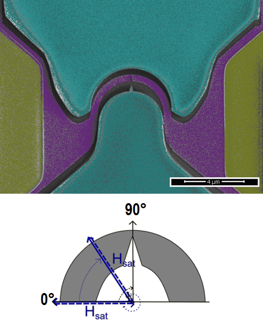
The experiments were carried out on polycrystalline permalloy (Py: Ni80Fe20) samples of 23 nm thickness, grown by thermal evaporation in a UHV chamber with a base pressure of mbar. In order to avoid certain parasitic contributions to the MR measurements, we use our previously established procedure to fabricate magnetic nanocontacts in clean UHV conditions von Bieren et al. (2013) and perform in-situ magnetic characterization, as outlined below. The size of the contact is subsequently tailored in-situ from the initial lithographically defined cross-section, which is a few tens of nm at the narrowest part, down to the single nm regime and below via a computer-regulated electromigration procedure Park et al. (1999); Esen and Fuhrer (2005); Hoffmann et al. (2008); Stöffler et al. (2012). At each stage, the MR behaviour is measured to determine the evolution of the properties with contact size. In order to avoid magnetostrictive contributions we choose Py as our magnetic material and use a notched half-ring geometry where we can control the presence and position of DWs in the structure at remanence, as depicted in Figure 1. The system and process of nanocontact fabrication are described in detail in Reeve et al. (2014). In the initial state, the contact is around nm wide at the notch position. Both electromigration and magnetotransport measurements are performed at temperatures around 80 K using a liquid nitrogen cryostat. In order to characterize the magnetoresitance we perform a so-called mode-étoile measurement Pfeiffer et al. (2017). A magnetic field of 150 mT is applied along a given angle, , using a vector magnet Krzyk et al. (2010) and then relaxed to zero, before measuring the two-point resistance of the contact at remanence. This process is then repeated for incrementally changing angles until the desired angular range is probed. The electromigration procedure is subsequently performed in order to narrow down the sample at the region of highest current density, which corresponds to the notch, as detected by the concurrent increase in resistance of the sample from the initial state of around 436 . The magnetotransport characterization is then carried out for the new contact state and the whole process is iterated until the contact size has been reduced to the expected sub-nm regime Reeve et al. (2014).
II.2 Density function theory calculations (DFT)
To theoretically understand the transport properties of the system semi-quantitatively, we have modeled Ni80Fe20 by Ni3Fe in the common faced-centered crystal structure (fcc). In the experiment, the transport at the narrow-constriction is likely to be dominated by a single grain Krzyk et al. (2010), while the 5 composition difference is not expected to give a significance change in the transport properties. In this configuration, the Fe atoms sit at the summit of the pseudo-cubic unit cell and the Ni atoms are at the center of the faces. The experimental pseudo-cubic lattice parameter Å was used. We have calculated the band structure with the full potential linearized augmented plane wave (FLAPW) basis set as implemented in the FLEUR 111www.flapw.de ab-initio package. We have used a cutoff of the plane wave basis set of bohr-1 and 560 k-points in the irreducible Brillouin zone. The band structure was obtained with the Perdew-Burke exchange and correlation Perdew et al. (1992).
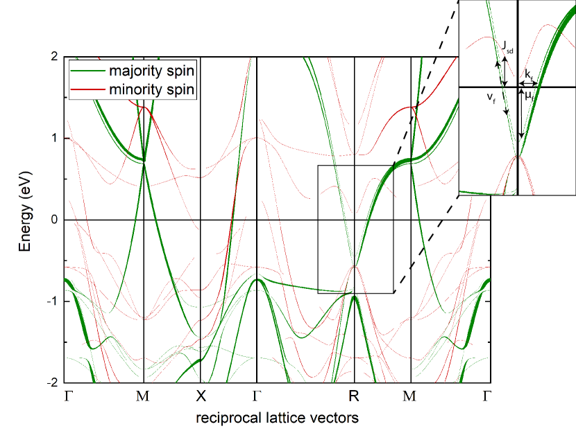
The band structure was extrapolated using maximally localized Wannier functions as implemented in the wannier90 package Marzari and Vanderbilt (1997); Souza et al. (2001); Mostofi et al. (2014). We have used 9 Wannier orbitals (1s, 3p and 5d) for each atom in the chemical unit cell for spin up and spin down. The bands were disentangled within an energy window up to 30 eV containing 50 bands and a frozen window up to 15 eV above the Fermi level Souza et al. (2001). To obtain the s-character contribution of the Bloch state shown in Figure 2, we have projected the resulting wannier orbitals on the s-wannier orbitals.
Figure 2 shows the s-character of the Bloch states along the high symmetry lines of a simple cubic lattice. The conduction bands are evenly spread along the high symmetry lines. To parametrize a simple tight-binding Hamiltonian, it is convenient to pinpoint bands which have the same orbital character and which are not degenerate at the Fermi level. The bands around the -point show these characteristics (Fig. 2 inset). We can then extract the Fermi velocity, , the s-d coupling, which corresponds to the band splitting at the Fermi level and the chemical potential . We have focused on the up and down spin channels at the Fermi level along the high symmetry line . We have extracted ms-1 which is of the same order of magnitude as typical metals Ashcroft and Mermin (1976), eV, bohr-1 and eV. These parameters were then used to parametrize an effective tight-binding Hamiltonian.
II.3 DC electrical conductivity from quantum simulations
To obtain insights into the domain wall magnetoresistance (DWMR), we perform transport calculations by solving the quantum-mechanical scattering in the ballistic regime for both spin channels through a domain wall. The ballistic regime approximation is justified by the spin diffusion length on the order of nm Bass and Jr (2007); Petrovykh et al. (1998) which has been measured in Ni80Fe20 and compares favourably with the experimentally estimated domain-wall sizes down to nm (see Ref. Reeve et al. (2014) and Fig. 5).
According to our DFT calculations the physical behaviour of low energies can be described by a surprisingly simple Hamiltonian, which is commonly referred to as the s-d model Zhang and Li (2004). In this approximation the -orbital is associated to the magnetic moments of permalloy which have a fixed position and direction, while the spin of the -electrons is scattered through the domain wall. In the case of non-collinear magnetization, such a model can be written as:
where is the hopping parameter, is the chemical potential, is the spin-splitting, is a unit vector at site and is the spinor of the -electron. To derive the suitable scattering transport parameters, we consider the band-structure of Ni3Fe, which was obtained by DFT calculations. The value of the eV and eV can be used directly but the ms-1 and bohr-1 have to be transformed to a hopping parameter . For a free electron, the dispersion is given by the simple relation:
| (2) |
where Å is the lattice parameter of bulk Ni3Fe. This relation can be used to obtain the Fermi velocity as a function of . We therefore obtain
| (3) |
This yields eV. The DFT calculations were done for a collinear magnetic texture. We impose the DW profile within the Hamiltonian from eq. II.3 via the -coupling. Without loss of generality, the magnetization is constrained in the plane and is given by:
| (4) |
where is the polar angle that changes from to over the DW’s width or a Néel DW.
In order to find the total resistance we have to average over the resistance for different incident particles with momentum over the 3D Fermi sphere Ashcroft and Mermin (1976); Stiles and Zangwill (2002),
| (5) |
where is the electron charge, is the velocity and is the Fermi-Dirac distribution. In our case, the scattering parameters only depend on the -components along the domain wall if the perpendicular components are approximately conserved. It is therefore sufficient to solve the 1D scattering problem using the usual plane-wave ansatz:
| (6) |
where the wave number is the projection of along the domain wall direction and we consider a completely up-spin-polarized current . Note that the reflection and transmission coefficients are also a function of incident momentum. Here the wave-numbers for up and down spin must be related by the dispersion relations
| (7) | ||||
| (8) |
Finally, knowing the resistance is directly proportional to the reflection coefficients, the resistance for each momentum can be determined from,
| (9) |
Since the scattering problem is solved for a number of incident particles with different momenta numerically, the integral is turned into a summation over the values obtained for a reasonably large number of incident particles (here we found out that 150 different -values suffice). From Eq. 5 and after going to polar coordinates, the resistance for each averaged over different momenta is simplified as,
| (10) |
where parameterizes the incoming direction and we have approximated with a delta function which is justified for the relevant parameter ranges. The results and their comparison to experiments are discussed in Sec. IV.
II.4 Micromagnetic Simulations
Micromagnetic simulations of the domain wall spin structure were performed using the multi-scale modified MicroMagnum code MM as described in Ref. De Lucia et al. (2016). Multiscale modelling is necessary to realistically model the spin structures even for very narrow domain walls. Standard parameters for permalloy were chosen, namely exchange energy constant, J/m3, anisotropy constant, and saturation magnetization, A/m. In-plane cell sizes of nm and nm were used for the coarse- and fine- scale regions, respectively, with the cell size normal to the plane equal to the film thickness. A high damping, , was used to speed up the convergence. In order to further save on simulation time we simulated just the central portion of the half-ring over an area of 2000720 nm and fixed the magnetization at both ends of the wire to be parallel to the wire axis, as expected from the shape anisotropy and confirmed previously by imaging of the spin structures. In the simulations this was achieved by applying a localized large field to the cells at the two edges. The fine-scale region of the simulation is applied to a region of 4040 nm for the portion of the wire where the confined DW is expected, based on initial coarse-scale simulations of the whole system. For most constriction widths this corresponds to the central notch region, however for the asymmetric transverse wall in the case of the smallest constriction, the fine-scale region was positioned on the outer-edge of the half-ring. To account for the effect of electromigration on the dimensions of the contact, as employed in the experiments to change the contact size, we reduce the width of the wire at the notch position and since the electromigration procedure is expected to reduce the size of the contact in all dimensions, for widths smaller than the initial wire thickness we also reduce the simulated wire thickness accordingly. To calculate the AMR contribution from the simulated magnetization configurations for states with and without a DW at the notch we perform simulations of the current distribution in the samples. From these, we calculate the difference in the resistance in each case, taking into account the angle between the magnetization and the current and assuming an AMR of around 1%, as in Ref. Beguivin et al. (2014).
III Results
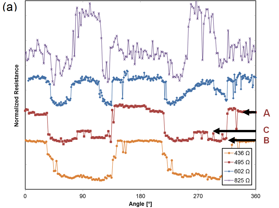
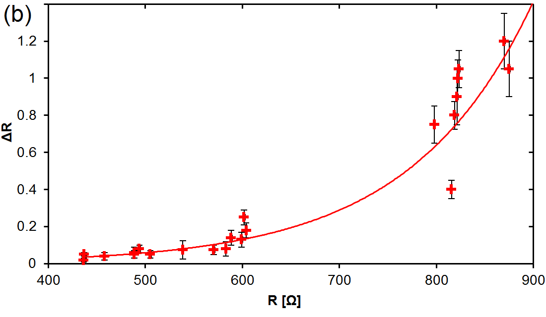
The results of the mode-étoile measurement for selective resistance states of the sample are presented in Figure 3 (a) Loescher (2013). For the initial state of the contact - i.e. the state with a resistance of 436 , the plot shows two main resistance levels as a function of the angle, which can be understood as follows: Depending on the angle of the saturating field, a domain wall may or may not be nucleated in the structure and as a result the two resistance states can be attributed to the presence and absence of a domain wall between the probes Patra et al. (2010). When the field is initially applied along angles in the range 325∘-035∘, or equivalently 145∘-215∘, the remnant configuration is expected to be a quasiuniform state with no domain wall in the half-ring. Conversely, for the remaining field ranges, a domain wall is expected to be nucleated from the larger pad regions and propagate into the half ring until it is aligned with the field. In this case, the resistance of the structure is seen to decrease when a domain wall is present. However as confirmed by previous work, for this initial size regime the reduction can be attributed primarily to the AMR effect which, due to the component of magnetization within the wall that is directed off-axis to the wire, leads to a reduction of the wire resistance. For the second resistance state (495 ) we still see the two previous levels corresponding to no domain wall () and a domain wall in the main part of the wire (), however a third level is now evident for angles in the vicinity of the direction of the notch position (90/270∘). For a half ring of constant width, the domain wall is expected to be nucleated close to the position of the applied field due both to the curved geometry, as well as to the soft magnetic properties of the Permalloy. However, in the presence of significant constrictions the domain wall can be attracted to the resulting potential well from a large distance away. Hence this resistance level can be attributed to a new resistance state for a domain wall within the notch (). As can be seen, with increasing resistance of the nanocontact, or equivalently for decreasing size of the contact at the notch, the resistance state corresponding to the DW in the notch in general becomes broader and larger. The change in resistance associated with the DW in the notch is plotted as a function of the resistance in Figure 3 (b). Here the resistance change, , is calculated as the size of the peak corresponding to the DW in the notch, normalized with respect to the level with no DW in the structure (). As such for there is a difference in the contact resistance for a DW in the wire and in the notch, whereas for the resistance for a DW in the notch is larger than that with no DW in the structure. Strikingly it can be seen that for the narrowest contacts the resistance of state , corresponding to a DW in the notch, even exceeds that of state A, and hence the effect can not be described solely based on a different size of the AMR for the particular spin state of the domain wall at the notch (which would reduce the resistance), but rather there must also exist an intrinsic DWMR contribution which dominates for this size regime. While previous work has reported both positive and negative DWMR for Py, here we find a positive effect for our contact sizes.
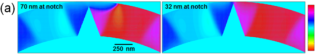
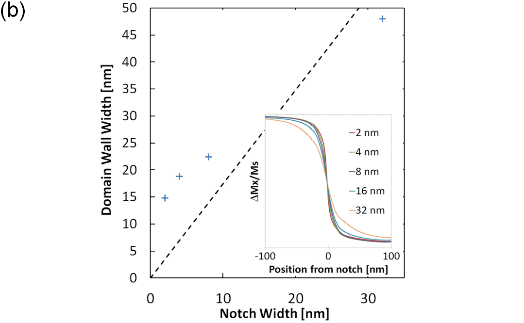
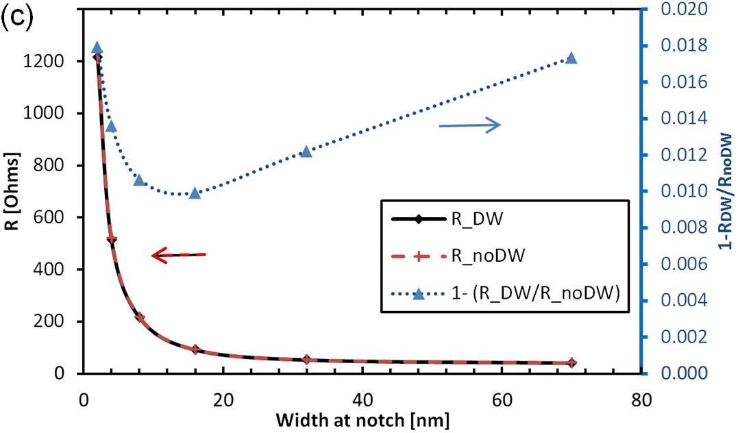
To gain insights into the evolution in the magnetic domain wall width with the nanocontact size, as well as the contribution from AMR, we perform multiscale micromagnetic simulations for the employed geometry. Figure 4 (a) presents typical simulations of the magnetization configurations as a function of the contact width, . In all cases a transverse domain wall spin configuration is formed, as expected from the dimensions of the wires Laufenberg et al. (2006) with a tilted transverse wall for the smaller notch evolving to a symmetric transverse wall for the larger notches, as previously observed in experiments Backes et al. (2007). Furthermore, as seen both in the images and in Figure 4 (b), the DW width, , shows a monotonic dependence on the nanoconstriction size. This scaling of the wall size with the geometrical confinement is consistent with the predictions of Bruno Bruno (1999), who showed that the increased exchange energy of the narrower wall is compensated by restricting the wall to a smaller volume, as has also been observed experimentally Jubert et al. (2004); Laufenberg (2006); Kläui (2008); Backes et al. (2007). The AMR contribution from the changing DW is shown in Figure 4 (c). In such a notched system, the magnitude of the AMR component is an interplay between the confinement of the DW, which reduces the off-axis magnetization components and the confinement of the current, which means that the signal is increasingly dominated from the central region. In our case we find that in general the AMR contribution from the DW increases for smaller constrictions. However the size of the AMR contribution is rather small, on the order of 1-2 %, in agreement with previous reports of AMR in Py nanocontacts Patra et al. (2010); von Bieren et al. (2013), with sub 1 % changes for evolving contact size within the studied range, which is much smaller than the total effects we observe, and hence we now consider alternative explanations for the DWMR we observe.
IV Discussion
In order to understand the data, it is instructive to fit the data to a power function of the following form, as predicted by theory Viret et al. (1996); Levy and Zhang (1997); Brataas et al. (1999); Bergeret et al. (2002); Kudrnovský et al. (2001); Yavorsky et al. (2002):
| (11) |
where is the domain wall resistivity, is the material resistivity and , are constants Viret et al. (1996). The resistivity of the domain wall can be defined based on the area of the contact, , and the domain wall width:
| (12) |
The contact radius, , can be estimated from the contact resistance via Wexler’s formula, which is an interpolation between the classical Maxwell expression of the conductance and the Sharvin expression valid in the ballistic regime Wexler (1966); Patra et al. (2010); Reeve et al. (2014):
| (13) |
is the electron mean-free path which is taken as 0.6 nm Petrovykh et al. (1998) and the resistivity of Permalloy is taken as m based on the relation in Ref. Bogart and Atkinson (2009). The value of is calculated from the measured two-point resistances, corrected for the effective lead-resistance, which is determined to be based on the initial contact dimensions Loescher (2013). The DW size is in turn calculated using the previously determined proportional scaling of the DW with wire width for rings Laufenberg (2006); Kläui (2008), presented in Figure 4 (b), which has reasonable agreement with the simulations performed here for our notched system. The resulting data are presented in Figure 5. For larger contacts, Equation 13 returns a relatively large error in the contact size and correspondingly also the domain wall size, since there is some uncertainty in the original lead resistance. However as the contact is narrowed down, the increase in resistance is expected to originate solely from the notch region where the current density is highest and the electromigration therefore occurs and hence the junction region resistance increasingly dominates the overall two-point resistance.
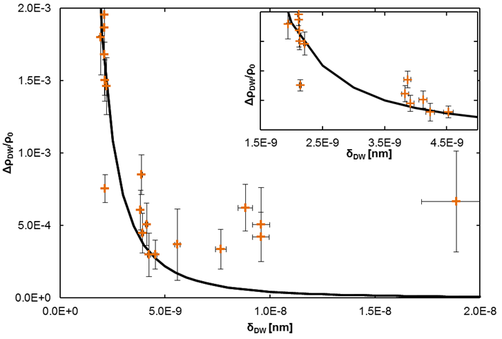
The line represents a fit to the data using Equation 11 which is weighted based on the strongly varying errors in the DW width Loescher (2013), yielding an exponent of . For the larger domain wall widths it can be seen that there is some deviation from the fit, with the data not tending to zero domain wall resistivity for the widest widths, indicative of additional contributions such as the AMR effect. However as confirmed by the micromagnetic simulations, the AMR effect is small for our geometry and does not dominate for the smaller constrictions. Furthermore, Yuan et. al predict the existence of an additional spin-orbit coupling induced contribution to the resistivity Yuan et al. (2012), which would lead to a similar plateau for large domain widths and would also be consistent with the presented data. The observation of an intrinsic positive DWMR that scales with the contact size in Py is in contrast to our previous measurements for both larger and smaller contacts, since in the former case only AMR dominated signals were determined Patra et al. (2010), whereas in the latter both positive and negative DWMR was seen, the size and sign of which was primarily determined by the atomic co-ordination at the contact position von Bieren et al. (2013). The scaling of the domain wall resistivity with domain wall size has been theoretically studied by a number of approaches Marrows (2005), with certain models predicting a positive contribution to the domain wall resistivity which has an inverse scaling relation with the domain wall size Viret et al. (1996); Levy and Zhang (1997); Brataas et al. (1999). A semi-classical model by Viret et al. considered the ability of an electron to track the local magnetization direction as it traverses a domain wall Viret et al. (1996). As the width of the wall decreases, the non-adiabaticity of the majority electron spin alignment with the local wall spin direction increases. Hence changes to the dynamic non-adiabaticity parameter of the system are also expected, as hinted at by experimental depinning measurements. In the model, the electrons precess in the locally canted exchange field of the DW and depending on the rate of precession and the magnetization gradient they can track the changes to a greater or lesser extent. The resulting mistracking results in extra scattering and a corresponding increase in the DW resistivity which was found to scale with the square of the domain wall width. An equivalent scaling has been predicted by Levy and Zhang who treated the problem quantum mechanically Levy and Zhang (1997) and showed that the mixing of the spin channels is the origin of the enhanced resistivity, and other works also arrive at similar results Brataas et al. (1999); Bergeret et al. (2002). In our case, the observed exponent of agrees with these theories. Similar results have been seen for the PMA Pt/Co/Pt system, where Ga ion implantation was employed to modifiy the anisotropy, , of the films and thereby set the DW width, which scales as , where is the exchange stiffness Franken et al. (2012). In that work also a dependence was determined. Here, we reveal a comparable scaling dependence for an in-plane system consisting of a single layer and with DW width tailoring via geometrical confinement.
We now use our theoretical calculations to understand the regimes of validity of the different behaviours in more detail. We perform theoretical calculations of DWMR by solving a quantum-mechanical scattering problem, as described in section II.3.
(a)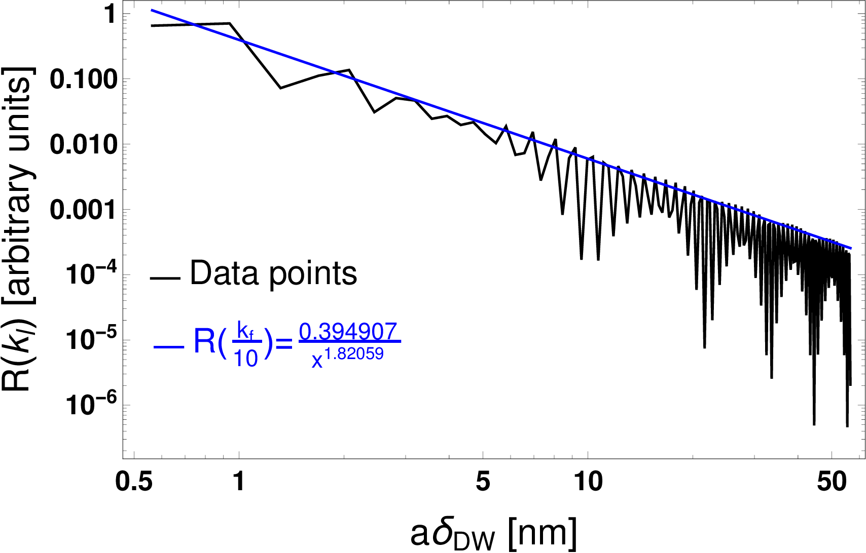 (b)
(b)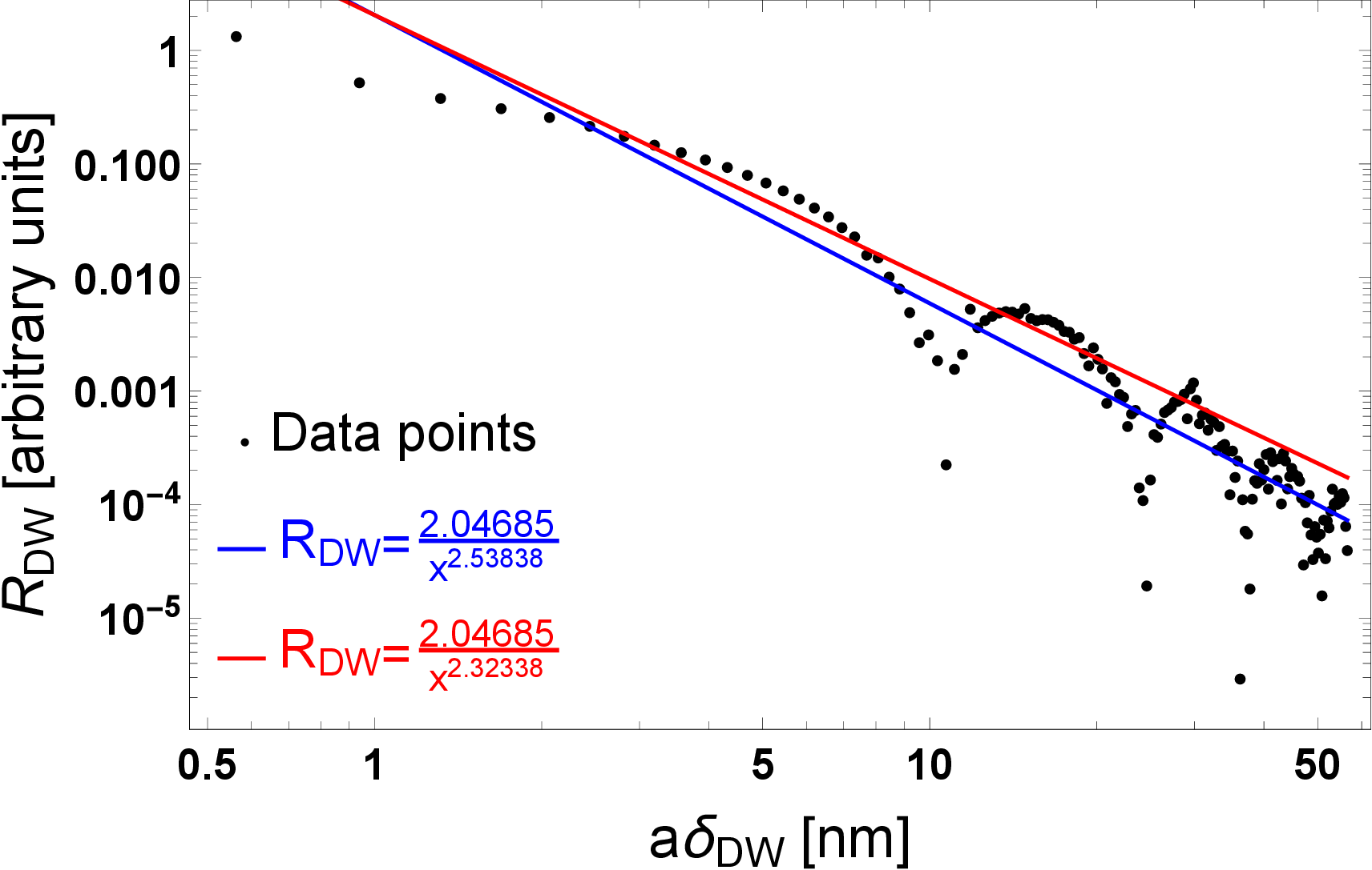
It can be seen that for a single given incoming wave-number there are characteristic oscillations in the reflection and transmission coefficients due to the precession of the electron spins that may or may not be commensurate with the domain wall width. The contribution of a single channel to the DWMR is depicted for in Fig. 6(a). The data for a single shows strong oscillations and a slow decay with which is changed by averaging over incoming directions in Eq. 10 . The resulting calculated total DWMR is plotted in Fig. 6(b) in a log-log plot. The fit to the data shows that the average fit to the DWMR scales as (blue line), and the fit to the maxima of the DWMR scales with (red line) in excellent agreement with our experiments and earlier theoretical results Tatara (2000); Allende et al. (2014); Kudrnovský et al. (2001); Yavorsky et al. (2002). This reveals that the observed scaling of the effects is robust and is preserved on transition from the diffusive Viret et al. (1996) to the ballistic regime as studied here and hence could be usefully employed in a device setting.
V Conclusion
In conclusion, we have studied the evolution in domain wall resistivity with the size of the domain wall in electromigrated permalloy nanocontacts. By employing a robust technique to create clean, magnetostriction-free nanowires with tailored size and with domain walls stable at remanence, we are able to demonstrate for narrow domain walls in narrow constrictions a clear positive intrinsic contribution to the domain wall resistivity which is not due to the anisotropic magnetoresistance effect. This finding is supported by micromagnetic simulations, which additionally demonstrate the geometrical confinement of the domain wall as the nanocontact is reduced in size by electromigration. The domain wall resistivity is found to scale with the domain wall width as , in excellent agreement with transport calculations which yield a dependence of , confirming increased scattering of the electrons as they traverse narrower domain walls which provide a more abrupt transition in the magnetization and hence a sharper potential step. While large domain wall magnetoresistance effects have previously been reported, they were often not particularly reliable or depended very delicately on the contact configuration. Hence the robust demonstration of a regime where large effects are seen and which scale monotonically with the geometrical confinement is of particular interest for proposed devices where notches are routinely employed as geometrical pinning centres for domain walls and where large magnetoresistance effects are beneficial.
Acknowledgments
Funded by the Deutsche Forschungsgemeinschaft (DFG, German Research Foundation) - project number 268565370/TRR173 through the collaborative research centre SFB/TRR 173 Spin+X, ”Spin in its collective environment” (Projects B02, A03 and A10) as well as the Graduate School of Excellence Materials Science in Mainz (GSC266). This work was supported in Rzeszów University of Technology by the National Science Center in Poland as research Project No. UMO-2017/27/B/ST3/02881.
References
- Binasch et al. (1989) G. Binasch, P. Grünberg, F. Saurenbach, and W. Zinn, Phys. Rev. B 39, 4828 (1989).
- Baibich et al. (1988) M. N. Baibich, J. M. Broto, A. Fert, F. N. Van Dau, F. Petroff, P. Etienne, G. Creuzet, A. Friederich, and J. Chazelas, Phys. Rev. Lett. 61, 2472 (1988).
- Julliere (1975) M. Julliere, Physics Letters A 54, 225 (1975).
- Bowen et al. (2001) M. Bowen, V. Cros, F. Petroff, A. Fert, C. Martı́nez Boubeta, J. L. Costa-Krämer, J. V. Anguita, A. Cebollada, F. Briones, J. M. de Teresa, L. Morellón, M. R. Ibarra, F. Güell, F. Peiró, and A. Cornet, Applied Physics Letters 79, 1655 (2001).
- McGuire and Potter (1975) T. McGuire and R. Potter, IEEE Transactions on Magnetics 11, 1018 (1975).
- Parkin et al. (2008) S. S. P. Parkin, M. Hayashi, and L. Thomas, Science 320, 190 (2008).
- Allwood et al. (2005) D. A. Allwood, G. Xiong, C. C. Faulkner, D. Atkinson, D. Petit, and R. P. Cowburn, Science 309, 1688 (2005).
- Shvets et al. (2008) I. V. Shvets, H. C. Wu, V. Usov, F. Cuccureddu, S. K. Arora, and S. Murphy, Applied Physics Letters 92, 023107 (2008).
- Kläui et al. (2005) M. Kläui, C. A. F. Vaz, J. A. C. Bland, W. Wernsdorfer, G. Faini, E. Cambril, L. J. Heyderman, F. Nolting, and U. Rüdiger, Phys. Rev. Lett. 94, 106601 (2005).
- Cabrera and Falicov (1974) G. G. Cabrera and L. M. Falicov, physica status solidi (b) 61, 539 (1974).
- Viret et al. (1996) M. Viret, D. Vignoles, D. Cole, J. M. D. Coey, W. Allen, D. S. Daniel, and J. F. Gregg, Phys. Rev. B 53, 8464 (1996).
- Levy and Zhang (1997) P. M. Levy and S. Zhang, Phys. Rev. Lett. 79, 5110 (1997).
- van Gorkom et al. (1999) R. P. van Gorkom, A. Brataas, and G. E. W. Bauer, Phys. Rev. Lett. 83, 4401 (1999).
- Wickles and Belzig (2009) C. Wickles and W. Belzig, Phys. Rev. B 80, 104435 (2009).
- Tatara and Fukuyama (1997) G. Tatara and H. Fukuyama, Phys. Rev. Lett. 78, 3773 (1997).
- Brataas et al. (1999) A. Brataas, G. Tatara, and G. E. W. Bauer, Phys. Rev. B 60, 3406 (1999).
- Marrows (2005) C. H. Marrows, Advances in Physics 54, 585 (2005).
- Kent et al. (2001) A. D. Kent, J. Yu, U. Rüdiger, and S. S. P. Parkin, Journal of Physics: Condensed Matter 13, R461 (2001).
- Dugaev et al. (2003) V. K. Dugaev, J. Berakdar, and J. Barnaś, Phys. Rev. B 68, 104434 (2003).
- Hickey et al. (2008) M. C. Hickey, D. Atkinson, C. H. Marrows, and B. J. Hickey, Journal of Applied Physics 103, 07D518 (2008).
- Allende et al. (2014) S. Allende, J. Retamal, D. Altbir, and J. d’Albuquerque e Castro, Journal of Magnetism and Magnetic Materials 355, 197 (2014).
- Patra et al. (2010) A. K. Patra, A. von Bieren, S. Krzyk, J. Rhensius, L. J. Heyderman, R. Hoffmann, and M. Kläui, Phys. Rev. B 82, 134447 (2010).
- Jacob et al. (2008) D. Jacob, J. Fernández-Rossier, and J. J. Palacios, Phys. Rev. B 77, 165412 (2008).
- Viret et al. (2006) M. Viret, M. Gabureac, F. Ott, C. Fermon, C. Barreteau, G. Autes, and R. Guirado-Lopez, The European Physical Journal B - Condensed Matter and Complex Systems 51, 1 (2006).
- Bolotin et al. (2006) K. I. Bolotin, F. Kuemmeth, and D. C. Ralph, Phys. Rev. Lett. 97, 127202 (2006).
- Chopra et al. (2005) H. D. Chopra, M. R. Sullivan, J. N. Armstrong, and S. Z. Hua, Nat. Mater. 4, 832 (2005).
- Viret et al. (2002) M. Viret, S. Berger, M. Gabureac, F. Ott, D. Olligs, I. Petej, J. F. Gregg, C. Fermon, G. Francinet, and G. L. Goff, Phys. Rev. B 66, 220401 (2002).
- Doudin and Viret (2008) B. Doudin and M. Viret, Journal of Physics: Condensed Matter 20, 083201 (2008).
- Müller et al. (2011) M. Müller, R. Montbrun, M. Marz, V. Fritsch, C. Sürgers, and H. v. Löhneysen, Nano Letters 11, 574 (2011).
- Mallett et al. (2004) J. J. Mallett, E. B. Svedberg, H. Ettedgui, T. P. Moffat, and W. F. Egelhoff, Phys. Rev. B 70, 172406 (2004).
- Egelhoff et al. (2004) W. F. Egelhoff, L. Gan, H. Ettedgui, Y. Kadmon, C. J. Powell, P. J. Chen, A. J. Shapiro, R. D. McMichael, J. J. Mallett, T. P. Moffat, M. D. Stiles, and E. B. Svedberg, Journal of Applied Physics 95, 7554 (2004).
- Valladares et al. (2013) L. Valladares, A. Dominguez, J. Aguiar, R. Reeve, T. Mitrelias, R. Langford, Y. Azuma, C. Barnes, and Y. Majima, Brazilian Journal of Physics 43, 209 (2013).
- Yoshida et al. (2009) K. Yoshida, A. Umeno, S. Sakata, and K. Hirakawa, Japanese Journal of Applied Physics 48, 120216 (2009).
- Untiedt et al. (2004) C. Untiedt, D. M. T. Dekker, D. Djukic, and J. M. van Ruitenbeek, Phys. Rev. B 69, 081401 (2004).
- Papanikolaou (2003) N. Papanikolaou, Journal of Physics: Condensed Matter 15, 5049 (2003).
- Yi (2004) G. Yi, Phys. Rev. B 69, 132405 (2004).
- Theeuwen et al. (2001) S. J. C. H. Theeuwen, J. Caro, K. I. Schreurs, R. P. van Gorkom, K. P. Wellock, N. N. Gribov, S. Radelaar, R. M. Jungblut, W. Oepts, R. Coehoorn, and V. I. Kozub, Journal of Applied Physics 89, 4442 (2001).
- Taniyama et al. (1999) T. Taniyama, I. Nakatani, T. Namikawa, and Y. Yamazaki, Phys. Rev. Lett. 82, 2780 (1999).
- Ruediger et al. (1998) U. Ruediger, J. Yu, S. Zhang, A. D. Kent, and S. S. P. Parkin, Phys. Rev. Lett. 80, 5639 (1998).
- Miyake et al. (2002) K. Miyake, K. Shigeto, K. Mibu, T. Shinjo, and T. Ono, Journal of Applied Physics 91, 3468 (2002).
- Ebels et al. (2000) U. Ebels, A. Radulescu, Y. Henry, L. Piraux, and K. Ounadjela, Phys. Rev. Lett. 84, 983 (2000).
- Kim et al. (1999a) S. Kim, Y. Otani, K. Fukamichi, S. Yuasa, M. Nyvlt, and T. Katayama, Magnetics, IEEE Transactions on 35, 2862 (1999a).
- Kim et al. (1999b) S. Kim, Y. Otani, K. Fukamichi, S. Yuasa, M. Nyvlt, and T. Katayama, Journal of Magnetism and Magnetic Materials 198–199, 200 (1999b).
- García et al. (1999) N. García, M. Muñoz, and Y.-W. Zhao, Phys. Rev. Lett. 82, 2923 (1999).
- Céspedes et al. (2004) O. Céspedes, A. Rocha, S. Lioret, M. Viret, C. Dennis, J. Gregg, S. van Dijken, S. Sanvito, and J. Coey, Journal of Magnetism and Magnetic Materials 272–276, Part 2, 1571 (2004), proceedings of the International Conference on Magnetism (ICM 2003).
- Khizroev et al. (2005) S. Khizroev, Y. Hijazi, R. Chomko, S. Mukherjee, R. Chantrell, X. Wu, R. Carley, and D. Litvinov, Applied Physics Letters 86, 042502 (2005).
- Giordano and Çetin (2004) N. Giordano and B. Çetin, physica status solidi (b) 241, 2404 (2004).
- Kläui et al. (2003) M. Kläui, C. A. F. Vaz, J. Rothman, J. A. C. Bland, W. Wernsdorfer, G. Faini, and E. Cambril, Phys. Rev. Lett. 90, 097202 (2003).
- von Bieren et al. (2013) A. von Bieren, A. K. Patra, S. Krzyk, J. Rhensius, R. M. Reeve, L. J. Heyderman, R. Hoffmann-Vogel, and M. Kläui, Phys. Rev. Lett. 110, 067203 (2013).
- Achilles et al. (2011) S. Achilles, M. Czerner, and I. Mertig, Phys. Rev. B 84, 054418 (2011).
- Bergeret et al. (2002) F. S. Bergeret, A. F. Volkov, and K. B. Efetov, Phys. Rev. B 66, 184403 (2002).
- Kudrnovský et al. (2001) J. Kudrnovský, V. Drchal, I. Turek, P. Středa, and P. Bruno, Surface Science 482-485, 1107 (2001).
- Yavorsky et al. (2002) B. Y. Yavorsky, I. Mertig, A. Y. Perlov, A. N. Yaresko, and V. N. Antonov, Phys. Rev. B 66, 174422 (2002).
- Franken et al. (2012) J. H. Franken, M. Hoeijmakers, H. J. M. Swagten, and B. Koopmans, Phys. Rev. Lett. 108, 037205 (2012).
- Bruno (1999) P. Bruno, Phys. Rev. Lett. 83, 2425 (1999).
- Jubert et al. (2004) P.-O. Jubert, R. Allenspach, and A. Bischof, Phys. Rev. B 69, 220410 (2004).
- Breitkreutz et al. (2014) S. Breitkreutz, I. Eichwald, J. Kiermaier, G. Hiblot, G. Csaba, W. Porod, D. Schmitt-Landsiedel, and M. Becherer, Journal of Applied Physics 115, 17D506 (2014), https://doi.org/10.1063/1.4864737 .
- Reeve et al. (2014) R. M. Reeve, A. Loescher, M.-A. Mawass, R. Hoffmann-Vogel, and M. Kläui, Journal of Physics: Condensed Matter 26, 474207 (2014).
- Park et al. (1999) H. Park, A. K. L. Lim, A. P. Alivisatos, J. Park, and P. L. McEuen, Applied Physics Letters 75, 301 (1999).
- Esen and Fuhrer (2005) G. Esen and M. S. Fuhrer, Applied Physics Letters 87, (2005).
- Hoffmann et al. (2008) R. Hoffmann, D. Weissenberger, J. Hawecker, and D. Stöffler, Applied Physics Letters 93, (2008).
- Stöffler et al. (2012) D. Stöffler, S. Fostner, P. Grütter, and R. Hoffmann-Vogel, Phys. Rev. B 85, 033404 (2012).
- Pfeiffer et al. (2017) A. Pfeiffer, R. M. Reeve, M. Voto, W. Savero-Torres, N. Richter, L. Vila, J. P. Attané, L. Lopez-Diaz, and M. Kläui, Journal of Physics: Condensed Matter 29, 085802 (2017).
- Krzyk et al. (2010) S. Krzyk, A. Schmidsfeld, M. Kläui, and U. Rüdiger, New Journal of Physics 12, 013001 (2010).
- Note (1) www.flapw.de.
- Perdew et al. (1992) J. P. Perdew, J. A. Chevary, S. H. Vosko, K. A. Jackson, M. R. Pederson, D. J. Singh, and C. Fiolhais, Phys. Rev. B 46, 6671 (1992).
- Marzari and Vanderbilt (1997) N. Marzari and D. Vanderbilt, Phys. Rev. B 56, 12847 (1997).
- Souza et al. (2001) I. Souza, N. Marzari, and D. Vanderbilt, Phys. Rev. B 65, 035109 (2001).
- Mostofi et al. (2014) A. A. Mostofi, J. R. Yates, G. Pizzi, Y.-S. Lee, I. Souza, D. Vanderbilt, and N. Marzari, Comput. Phys. Commun. 185, 2309 (2014).
- Ashcroft and Mermin (1976) N. W. Ashcroft and N. D. Mermin, Solid State Physics, holt-saunders international ed. (Holt, Rinehart and Winston, 1976).
- Bass and Jr (2007) J. Bass and W. P. P. Jr, Journal of Physics: Condensed Matter 19, 183201 (2007).
- Petrovykh et al. (1998) D. Y. Petrovykh, K. N. Altmann, H. Höchst, M. Laubscher, S. Maat, G. J. Mankey, and F. J. Himpsel, Applied Physics Letters 73, 3459 (1998), https://doi.org/10.1063/1.122796 .
- Zhang and Li (2004) S. Zhang and Z. Li, Physical Review Letters 93, 127204 (2004).
- Stiles and Zangwill (2002) M. D. Stiles and A. Zangwill, Physical Review B 66, 014407 (2002).
-
(75)
MicroMagnum software,
http://micromagnum.informatik.uni-hamburg.de/ . - De Lucia et al. (2016) A. De Lucia, B. Krüger, O. A. Tretiakov, and M. Kläui, Phys. Rev. B 94, 184415 (2016).
- Beguivin et al. (2014) A. Beguivin, H. Corte-León, A. Manzin, V. Nabaei, P. Krzysteczko, H. W. Schumacher, D. Petit, R. P. Cowburn, and O. Kazakova, Journal of Applied Physics 115, 17C718 (2014).
- Loescher (2013) A. Loescher, Confined Domain Walls in Magnetic Nanocontacts, diploma thesis, Johannes Gutenberg Universität Mainz (2013).
- Laufenberg et al. (2006) M. Laufenberg, D. Backes, W. Bührer, D. Bedau, M. Kläui, U. Rüdiger, C. A. F. Vaz, J. A. C. Bland, L. J. Heyderman, F. Nolting, S. Cherifi, A. Locatelli, R. Belkhou, S. Heun, and E. Bauer, Applied Physics Letters 88, 052507 (2006).
- Backes et al. (2007) D. Backes, C. Schieback, M. Kläui, F. Junginger, H. Ehrke, P. Nielaba, U. Rüdiger, L. J. Heyderman, C. S. Chen, T. Kasama, R. E. Dunin-Borkowski, C. A. F. Vaz, and J. A. C. Bland, Applied Physics Letters 91, 112502 (2007).
- Laufenberg (2006) M. Laufenberg, Interactions Between Current and Domain Wall Spin Structures, Ph.D. thesis, Universität Konstanz (2006).
- Kläui (2008) M. Kläui, Journal of Physics: Condensed Matter 20, 313001 (2008).
- Wexler (1966) W. Wexler, Proc. Phys. Soc. London 89, 927 (1966).
- Bogart and Atkinson (2009) L. K. Bogart and D. Atkinson, Applied Physics Letters 94, 042511 (2009).
- Yuan et al. (2012) Z. Yuan, Y. Liu, A. A. Starikov, P. J. Kelly, and A. Brataas, Phys. Rev. Lett. 109, 267201 (2012).
- Tatara (2000) G. Tatara, J. Phys. Soc. JPN. 69, 2969 (2000).