Suppression of the Shear Raman Mode in Defective Bilayer MoS2
Abstract
We investigate the effects of lattice disorders on the low frequency Raman spectra of bilayer MoS2. The bilayer MoS2 was subjected to defect engineering by irradiation with a 30 keV He+ ion beam and the induced morphology change was characterized by transmission electron microscopy. With increasing ion dose the shear mode is observed to red-shift and it is also suppressed sharply compared to other Raman peaks. We use the linear chain model to describe the changes to the Raman spectra. Our observations suggest that crystallite size and orientation are the dominant factors behind the changes to the Raman spectra.
As research on transition metal dichalcogenides (TMDs) blooms Novoselov et al. (2016); Jariwala et al. (2016); Kang et al. (2017); Sung et al. (2017), it is crucial to understand the interfacial dynamics of these layered semiconductors in the few-layer limit. Low-frequency interlayer vibrational Raman modes serve as a fingerprint of the interlayer interactions between van der Waals-bonded sheets in both homo- and heterostructures Boukhicha et al. (2013); Lui et al. (2015); Zhang et al. (2016); Li et al. (2016). The low-frequency Raman modes of MoS2 include the in-plane shear mode (SM) and the out-of-plane layer breathing mode (LBM). Layer thickness, stacking order and angular lattice mismatch can be directly probed in vertically-assembled heterostructures of TMDs by investigating changes to these modes Zhao et al. (2013); Zhang et al. (2013); Lui et al. (2015); Zhang et al. (2015); Lin et al. (2016); Song et al. (2016). On the other hand, Raman spectroscopy has remained a high-throughput and non-destructive way of analyzing defects in MoS2 flakes in the last decade. In particular, the (385 cm-1) and (403 cm-1) modes are routinely used to identify layer thickness in exfoliated and deposited MoS2 samples Lee et al. (2010); Li et al. (2012); Zhang et al. (2013); O’Brien et al. (2015); Zeng et al. (2012). Relative changes in intensities, positions or widths are used to characterise the lattice modification of MoS2 Fox et al. (2015); Ko et al. (2016); Choudhary et al. (2016); Maguire et al. (2018). However, the effects of lattice defects on the low-frequency (50 cm-1) modes of few-layer MoS2 have not been explored, even while low-frequency Raman spectroscopy should play a vital role in the characterization of interfacial dynamics of defective layered semiconductors.
Herein we analyze the low-frequency modes of the Raman spectrum of bilayer MoS2 as a function of increasing disorder introduced by He+ irradiation at a beam energy of 30 keV. The helium ion microscope has been established as a tool for site-specific modification of 2D materials Fox et al. (2015); Zhou et al. (2016); Nanda et al. (2015); Iberi et al. (2016); Stanford et al. (2016, 2017); Nanda et al. (2017). It has been used to precisely introduce defects Maguire et al. (2018), fabricate nanoribbons and periodic arrays of nanodots Fox et al. (2015); Zhou et al. (2016) and introduce doping on the nanoscale Nanda et al. (2015).
MoS2 was prepared using a previously reported chemical vapor deposition (CVD) technique O’Brien et al. (2014). Bilayer flakes of MoS2 were identified on the SiO2 surface by optical contrast and Raman spectroscopy Lee et al. (2010); Castellanos-Gomez et al. (2012). The Zeiss ORION NanoFab microscope was used to irradiate arrays of 44 m2 regions in MoS2 with He+ at an energy of 30 keV and an angle of incidence of 0∘. These regions received doses ranging from 81013 to 21016 He+ cm-2. Further details of the ion irradiation are provided in the supplementary material. Ex-situ Raman and PL spectroscopy was carried out using a WITec Alpha 300R system (532 nm laser) with a 1800 lines/mm diffraction grating and a 100 objective (NA=0.95) (spot size 0.3 m). The instrument was equipped with a rayshield coupler to detect Raman signal close to the Rayleigh line. The laser power was 170 W or less to minimise damage to the samples. Raman and PL maps were generated by taking four spectra per m in both the x and y directions over large areas. The acquisition time was 0.113 s. The spectra from a desired region were acquired by averaging. Raman, PL and optical images are shown in Figure S1. Lorentzian distributions were fitted to the Raman peaks as demonstrated in Figure S4.
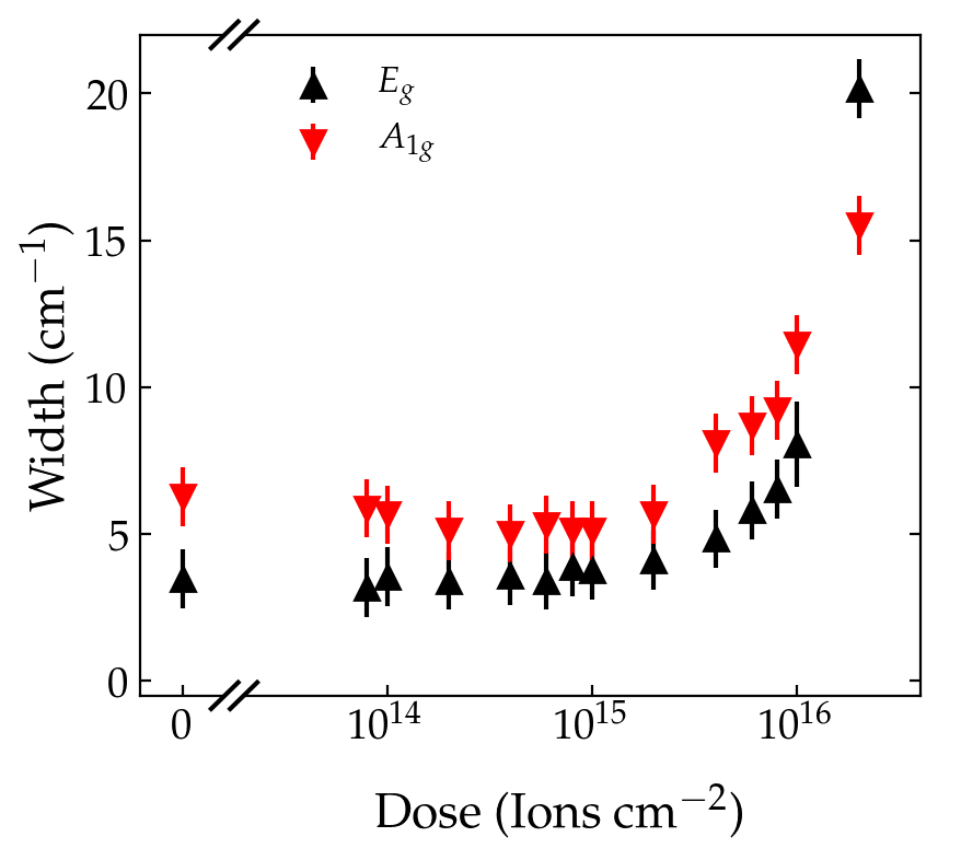
Figure 1 shows representative Raman spectra. In the low frequency region (Fig 1(a)), the SM and LBM peaks are centred at 41.0 cm-1 and 23 cm-1 respectively, which are in excellent agreement with the reported values for bilayer MoS2 Zhao et al. (2013); Zeng et al. (2012); Liang et al. (2017a). For increasing dose, the SM is clearly observed to red-shift and broaden while the LBM does not appear to change. At higher doses (1 He+ cm-2) the low frequency modes become indistinguishable from noise. In the high frequency region (Fig 1b), the characteristic and peaks of bilayer MoS2 are found at cm-1 and cm-1 respectively, thus exhibiting a high frequency peak separation of 22.6 cm-1 typical of CVD bilayer MoS2 Lee et al. (2010); Liu et al. (2014). With increasing ion dose the the peak is observed to broaden while the peak broadens, splits and is shifted downward in energy as has been reported before in similar conditions Mignuzzi et al. (2015); Klein et al. (2018); Maguire et al. (2018).
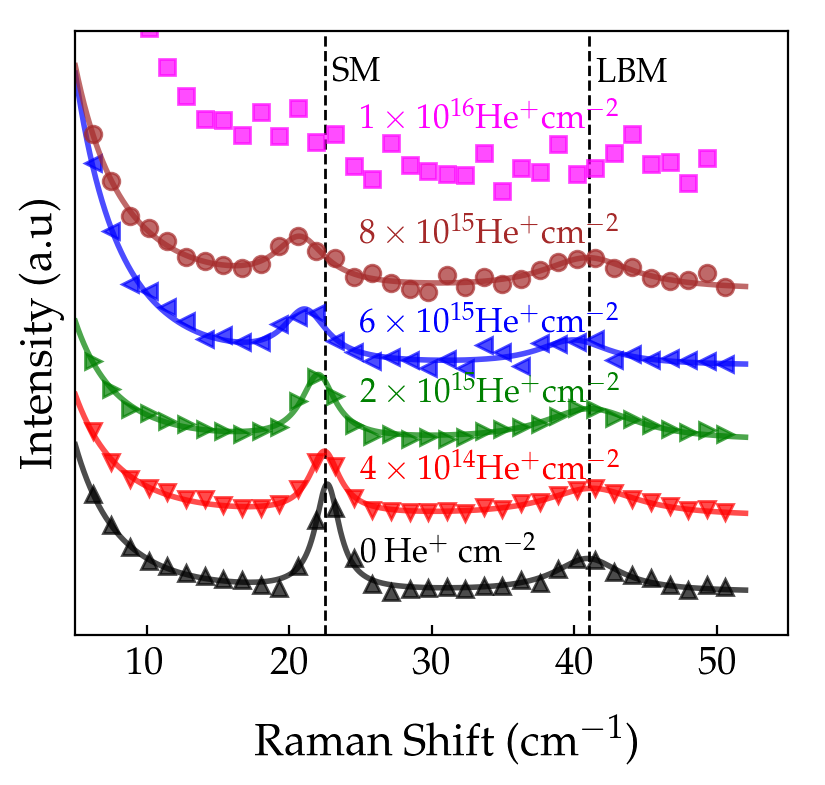
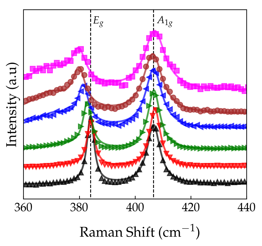
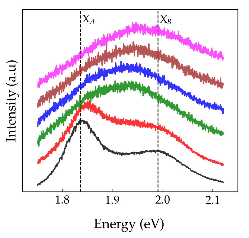
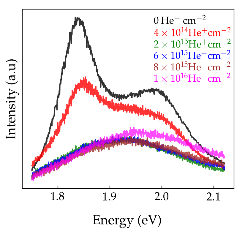
Figure 2 shows photoluminescence (PL) spectra acquired from the same regions of bilayer MoS2. We observe peaks at 1.85 eV and 2.01 eV, corresponding to the and direct excitonic transitions respectively Splendiani et al. (2010). The increased disorder is strongly associated with a lower quantum efficiency. The decrease in the exciton peak intensity is accompanied by a blue-shift which is attributed to strain caused by ion-induced defects Scheuschner et al. (2014). Above a dose of 2 He+ cm-2 we can no longer observe a clearly defined emission peak.
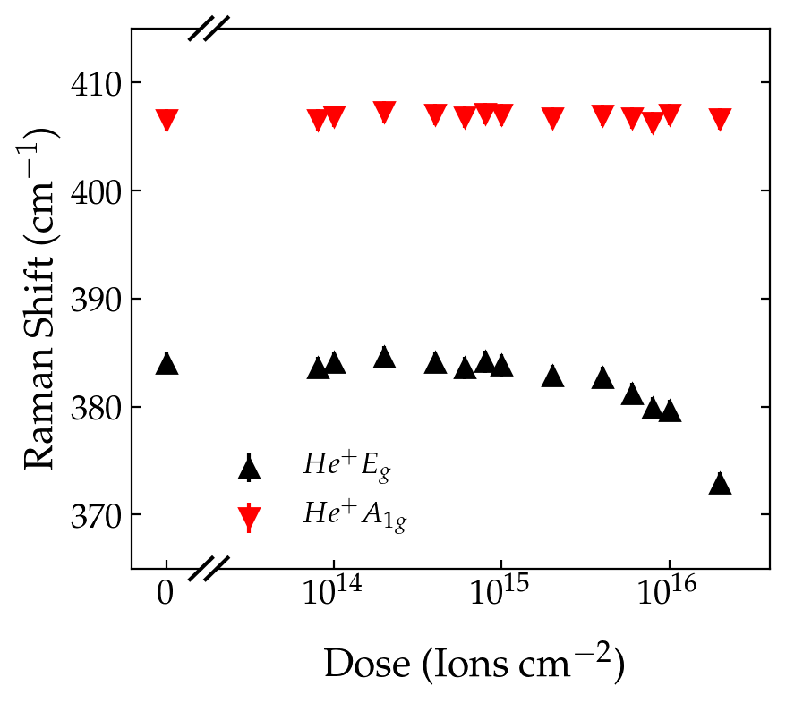
Figures 3(a) and (b) show the position and width respectively of the low frequency Raman peaks as a function of ion dose (analysis of the high frequency peaks is presented in Figure S3). The SM clearly shifts downward in position while it broadens. However, the LBM does not appear to change systematically in position or width. The measured SM frequency, , is given by
| (1) |
where cm-1 is the frequency of the non-irradiated bilayer MoS2 and is the ion dose (He+ cm-2). The measured width, , is given by
| (2) |
where cm-1 is the width of the undamaged bilayer MoS2.
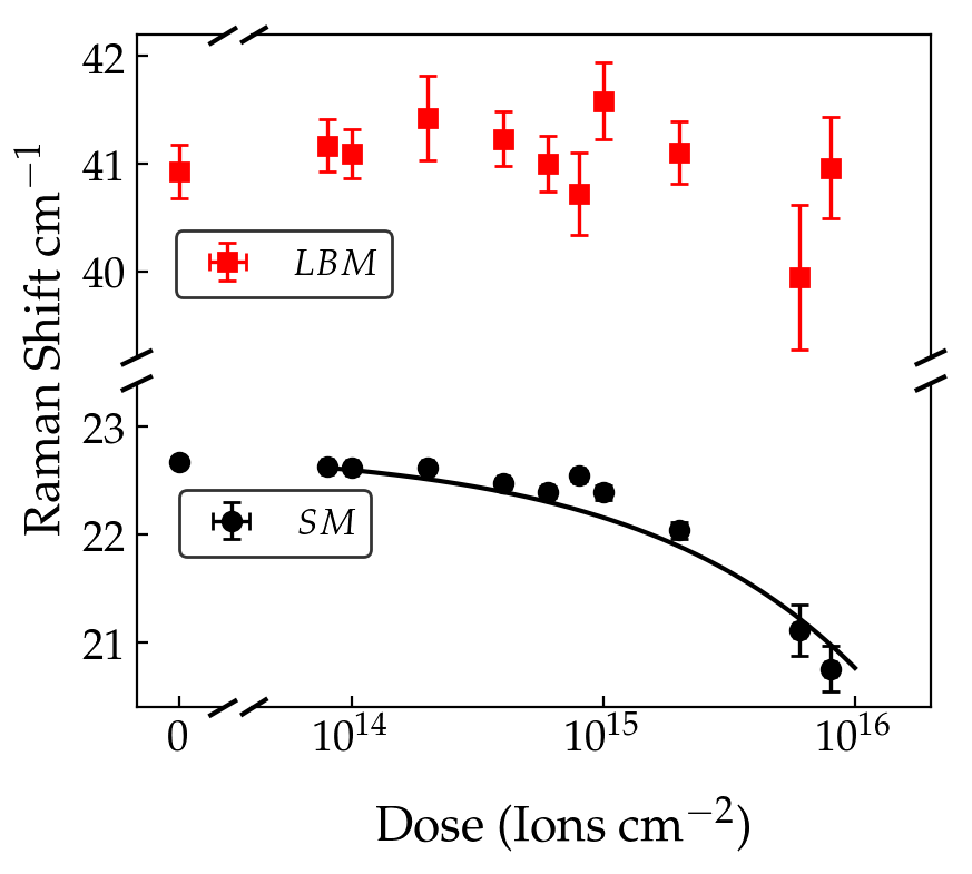
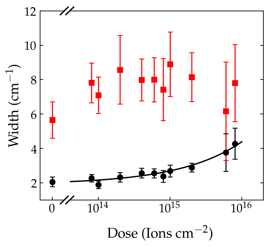
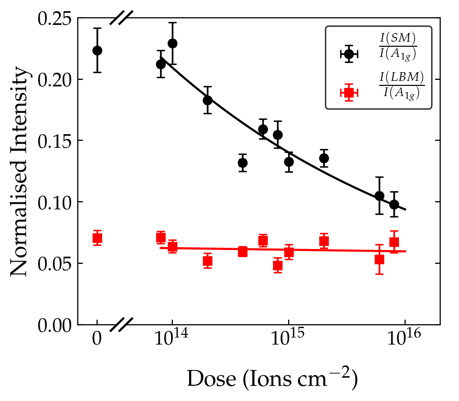
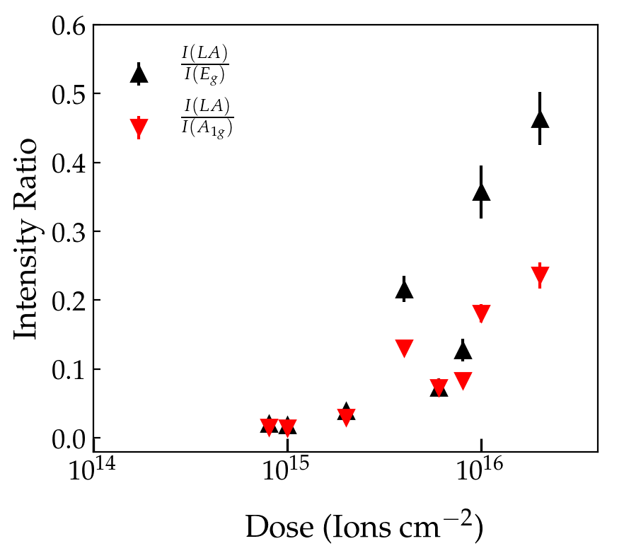
Figure 3(c) shows the heights of the low frequency modes, where = SM or LBM, normalized to the respective intensity, I(). While the intensity of is virtually constant, is observed to diminish with increasing dose. The SM is clearly suppressed more rapidly than other peaks by increasing disorder. The SM intensity ratio varies with the dose , where is a fitting parameter.
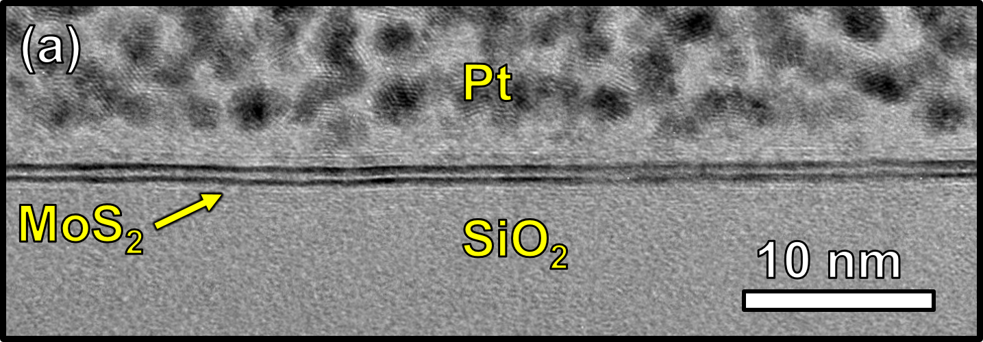
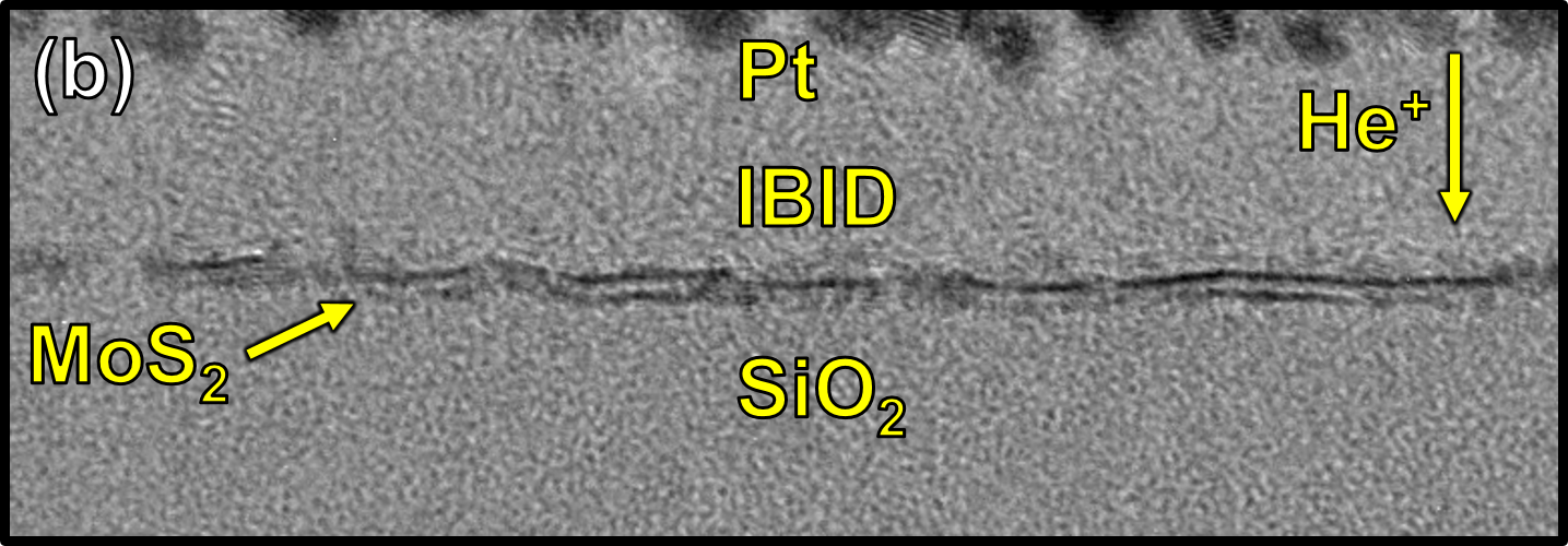
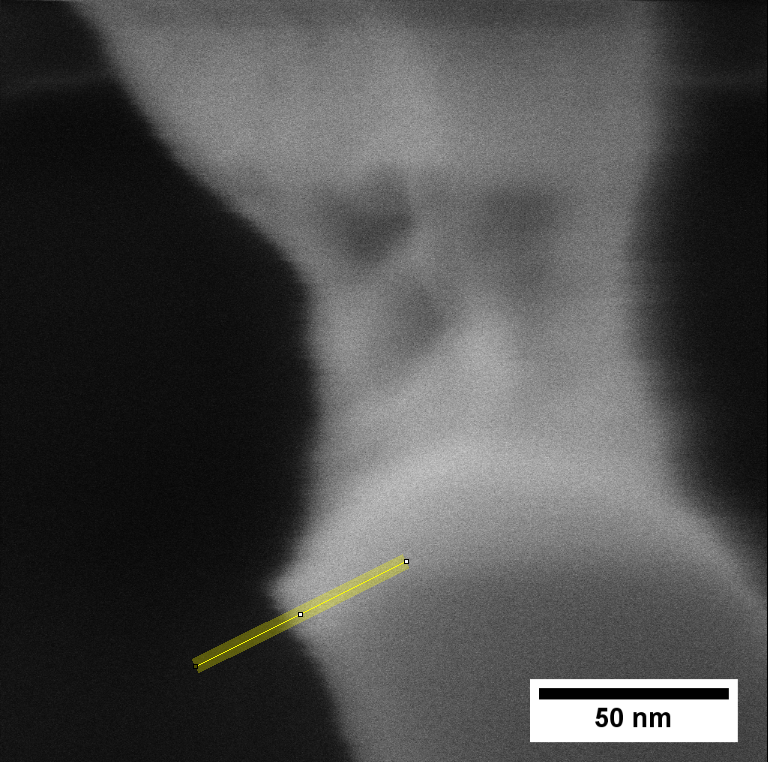
Figure 4(a) is a high resolution transmission electron microscopy (HRTEM) image of mechanically exfoliated bilayer MoS2 showing clearly defined layers with uniform interlayer spacing (see supplementary material including Figure S5 for TEM sample preparation). Above and below the MoS2, the protective platinum layer and the SiO2 substrate are visible, respectively. Figure 4(b) shows a region of the same sample which has been irradiated with 6 He+ cm-2 which is in the middle-to-high part of the range of doses used in our spectoscopic experiments. An additional amorphous hydrocarbon layer of helium ion beam-induced deposition (IBID) is visible on top of the MoS2. A clear increase in the surface asperity is noted after irradiation. In certain regions, MoS2 is still visibly present but separate layers cannot be resolved. This may suggest amorphization or local twisting of the layers such that they are imaged off-axis.
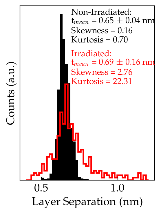
Figure 4(c) is a histogram of interlayer separation evaluated from the two TEM images, using a fitting process described in the supplementary material. There appears to be very little change in the mean layer separation after irradiation. However, the disordered distribution is clearly more diffuse and skewed towards higher values, reflected in the increased kurtosis and skewness respectively.
 (a)
(a)
 (b)
(b)
 (c)
(c)
A linear chain model (LCM) has been used to describe interlayer restoring forces by treating each layer as a rigid ball Zeng et al. (2012); Tan et al. (2012). The model has accurately predicted the frequencies of the low frequency modes in pristine MoS2 as a function of layer number. The single layer mass per unit area () of pristine MoS2 is 3.03 kg Å-2. The effects of irradiation-induced sputtering are accounted for in by applying an approximate correction related to the ion dose. Given the dose, , and the sputter yield, (=0.007 from previous reportsMaguire et al. (2018); Kretschmer et al. (2018); Parkin et al. (2016)), then for irradiated MoS2 is given by where n is the atomic density. This gives the sputtering-corrected LCM as:
| (3) |
where is the speed of light in cm s-1, is the layer number (fixed at 2 in this work), is the interlayer force constant per unit area which is related to the interlayer separation, , and the shear modulus, by . The separation of two non-irradiated layers in bilayer MoS2 measured from our TEM results is nm, in good agreement with literature Zeng et al. (2012). The shear modulus has been reported as 17.9 GPa Zeng et al. (2012). For = 0, the shear mode position is calculated to be 23.2 cm-1 which is consistent with our experimental value of 22.8 cm-1.
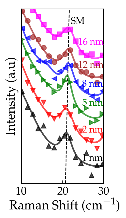
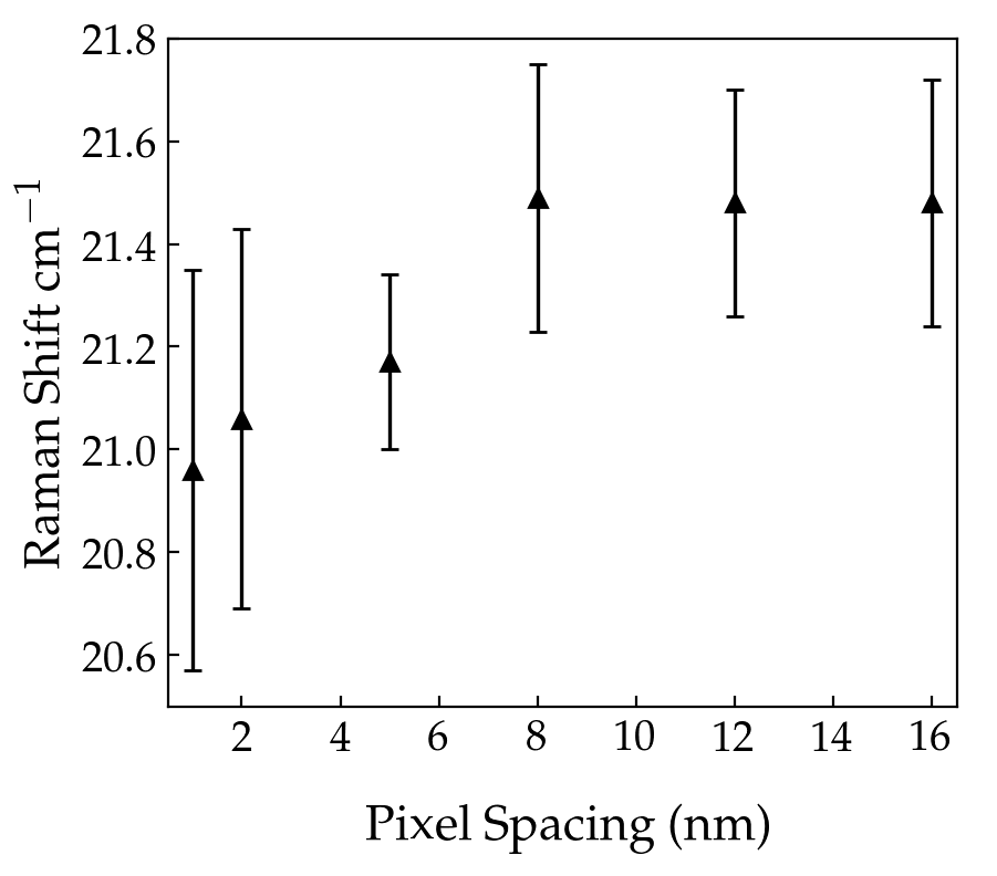
The two key findings of our Raman spectroscopy experiments clear from Figures 1 and 2 are related to the shear mode, i.e. the drop in the normalized intensity (2.3) and the frequency red-shift ( cm-1) with ion irradiation. Small twisting angles can introduce a periodicity mismatch between layers, altering the stacking configuration and causing a sharp decay of SM intensity and a downward shift in position Huang et al. (2016); Liang et al. (2017b). The twisting is evident in the TEM observation (Figure 4). However, the twisting alone cannot explain the observed peak shift (see Figure S10). Reductions in the shear modulus also contribute to a red-shift in the SM. This is due to the reduced crystallinity in MoS2 under ion irradiation. The reduced crystallinity leads to better lubricating properties, attributed to a greater tendency to exfoliate and therefore a reduced shear modulus Lahouij et al. (2012). To further corroborate this, we studied the effect of varying the pixel spacing on the SM with a new set of irradiation experiments. We used a fixed dose of 61015 cm-2 but we varied the pixel spacing from 1 to 16 nm. The probe size was 4 nm (see Figure S7) Rueden et al. (2017). The resulting Raman spectra are presented in Figure 6(a). Figure 6(b) shows that as the pixel spacing decreases, the red-shift of the SM is observed to increase (total effect is approximately 0.5 cm-1). As pixel spacings decrease, the total undamaged area is reduced. This suggests that regions of defective MoS2 may have a reduced shear modulus in addition to the twisting effects.
In conclusion, we explored the effects of increased disorder on the low and high frequency Raman peaks of bilayer MoS2. In the low frequency range, we noticed that the shear mode red-shifted and dropped in intensity with increased irradiation dose. We used TEM imaging to investigate and we suggest that these changes can be attributed to a mixture of local twisting of layers and a decline in the shear modulus due to reduced crystallite sizes.
Supplementary material is available at **. The authors thank the staff at the Advanced Microscopy Laboratory (AML), CRANN, Trinity College Dublin. We acknowledge support from the following grants: Science Foundation Ireland [grant numbers: 12/RC/2278, 15/SIRG/3329, 11/PI/1105, 07/SK/I1220a, 15/IA/3131, 08/CE/I1432 and GOIPG/2014/972].
Supplementary Information
I Maps and PL
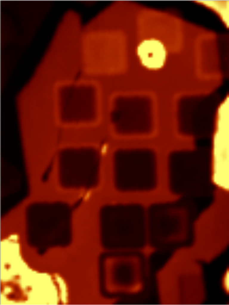
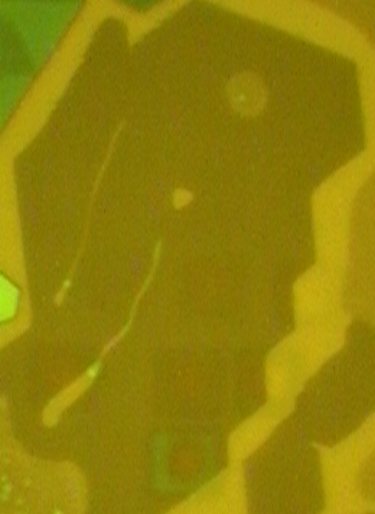
Figure S1 (a) is an example of one of the acquired Raman maps of bilayer MoS2, presented in this case by summing the intensity of the peak. The bright yellow color represents regions of high intensity. Several darker square regions are visible which were irradiated with different doses of the 30 keV He+ beam. Some other darker regions are monolayer parts of the sample and the darkest regions are the uncovered substrate. Spectra were extracted from sub-regions at least several hundred nanometres from the edges of the flake or the boundaries of the irradiated area and averaged. Figure S1 (b) is a PL intensity map of the same region. Figure S1 (c) is a white light optical image of the same region where the irradiated regions are only very faintly visible. Figure S2 is the same PL data as in Figure 2 but presented without normalisation.
II High Frequency Modes and Dose
Figure S3 (a) and (b) show the position and width respectively of the and peaks as a function of ion dose. There is no clear upshift in the peak compared to that observed for the peak in similar experiments in monolayer MoS2 Maguire et al. (2018). This may be caused by the bottom layer being protected from exposure to atmosphere (adsorption at defect sites can cause a blue shift). By contrast, the red shifts quite considerably for the higher doses, exhibiting very similar results to the peak in monolayer MoS2 Maguire et al. (2018). Both the and peaks increase in width as the ion dose increases as expected.
Figure S3 (c) shows the increasing intensity of the peak normalized to both the and peaks as a function of dose. As established by Mignuzzi et al., this represents an unambivalent decrease in the average distance between defects Mignuzzi et al. (2015).
III Raman Spectroscopy and Fitting
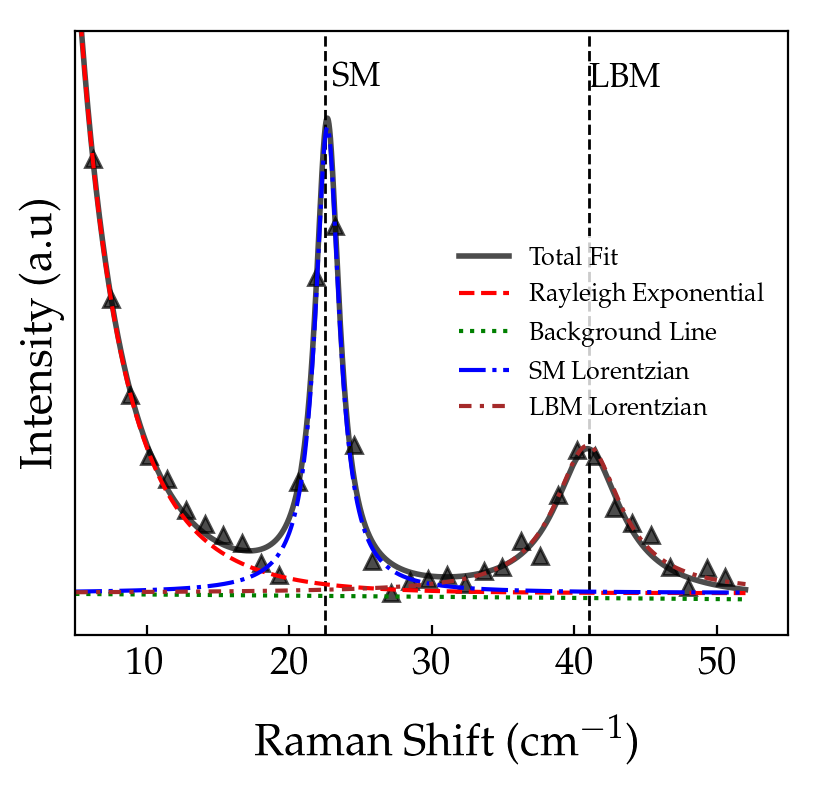
The fitting was performed using the curve_fit function in the scipy package in python. The bounds and seed values are provided in tables S1 and S2 for the low and high ranges respectively. Illustrations are provided in Figure S4. Error bars are from the fitting error. For the low frequency part, points below 5 cm-1 and above 51 cm-1 were excluded. The total equation used to fit to the low frequency part of the spectra is given by
| (S1) |
Where is the wavenumber (on the x-axis), is the intensity scale of the Rayleigh peak, is related to the decay of the Rayleigh peak, is the slope of the baseline, is the is the constant of the baseline, is the intensity of the SM, is the frequency about which the SM is centred, is the HWHM of the SM, is the intensity of the LBM, is the frequency about which the LBM is centred and is the HWHM of the LBM.
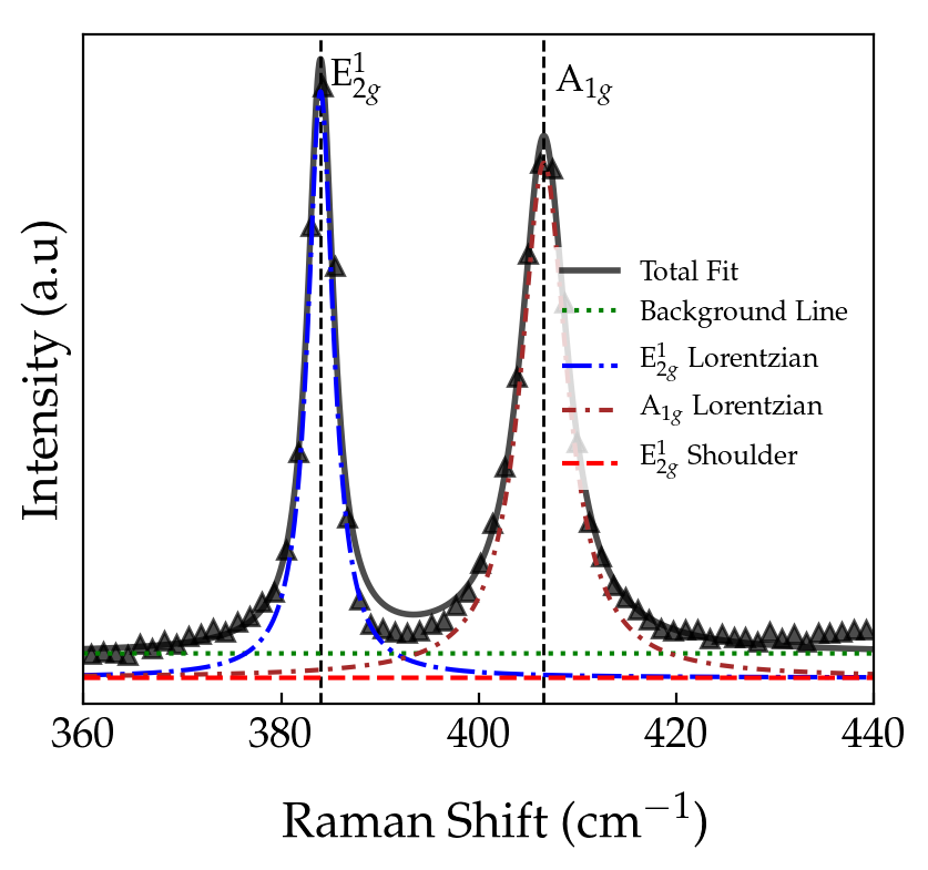
For the high frequency part, points below 360 cm-1 and above 440 cm-1 were excluded. The total equation used to fit to the high frequency part of the spectra is given by
| (S2) |
Where is the slope of the baseline, is the wavenumber (on the x-axis), is the is the constant of the baseline, is the intensity scale of the shoulder peak, is the frequency about which the shoulder peak is centred, is the HWHM of the shoulder peak, is the intensity of the peak, is the frequency about which the peak is centred, is the HWHM of the peak, is the intensity of the peak, is the frequency about which the peak is centred and is the HWHM of the peak.
| Labels | Limit | Initial | Limit | Unit | ||
|---|---|---|---|---|---|---|
| 0 | 10 | a.u. | ||||
| 0 | 0.7 | |||||
| -1E-4 | 100 | |||||
| -1E-4 | 100 | a.u. | ||||
| 0 | 1 | a.u. | ||||
| 0 | 100 | cm-1 | ||||
| 0 | 100 | cm-1 | ||||
| 0 | 1 | a.u. | ||||
| 1 | 10 | cm-1 | ||||
| 15 | 45 | cm-1 |
| Labels | Limit | Initial | Limit | Unit | ||
|---|---|---|---|---|---|---|
| 0 | 0.01 | |||||
| 0 | 100 | a.u. | ||||
| 0 | 200 | a.u. | ||||
| 1 | 100 | cm-1 | ||||
| 200 | 400 | cm-1 | ||||
| 0 | 300 | a.u. | ||||
| 1 | 100 | cm-1 | ||||
| 200 | 460 | cm-1 | ||||
| 0 | 300 | a.u. | ||||
| 1 | 100 | cm-1 | ||||
| 200 | 380 | cm-1 |
IV Lamella Preparation
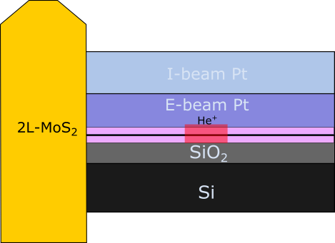
MoS2 for electron microscopy was mechanically exfoliated using the adhesive tape method from commercially available bulk molybdenite crystals (SPI Supplies). This method was chosen for the low level of pre-existing defects. Suitable flakes were identified and irradiated in similar fashion to the Raman experiments as shown in the optical image of Figure S5 (a). The flakes were deposited on a 285 nm layer of SiO2 on Si and bilayer regions with straight edges were identified using optical microscopy. A suitable flake was then irradiated in the Zeiss ORION Nanofab with a dose of 6 He cm-2. The pixel spacing was 5 nm and the beam current was 1 pA.
To prepare the cross-sectional lamella, the sample was loaded into a Zeiss Auriga focused ion beam system. The surface was covered locally with several hundred nanometres of a protective platinum-based coating, first using an electron beam at 5 keV and then using the 30 keV Ga+ beam. The lamella was cut using the Ga+ ion beam at 30 keV and lifted out using a nanomanipulator needle and welded to a copper TEM grid. Initial thinning was performed with a 15 keV Ga+ beam.
The sample was then cleaned for 90s in a Fischione Instruments 1020 plasma cleaner which uses a 1:3 mixture of O2/Ar gas. The sample was further thinned using a Fischione 1040 Nanomill. Argon ions at 900 eV and a beam current of 100 pA were incident at an angle of 70 degrees from the bottom (Si) of the lamella. The thickness was checked between each irradiation in the TEM. One side was irradiated for 13 mins total and the other for 4 mins total. The finished lamella is illustrated in S5 (b).
Electron microscopy was then carried out on the mechanically exfoliated bilayer MoS2 in a FEI Titan 80-300 operated at 300 keV with a chamber pressure of 4 10-8 mbar.
V Layer Separation Measurement
A python script was written which does the following:
-
•
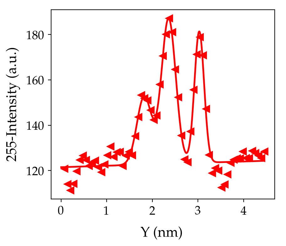
reads the columns of a TEM image (such as those in the main text) as line profiles and averages them over 2 pixels to each side to reduce noise.
-
•
fits three Gaussian distributions to each line profile (as demonstrated in Figure S6) corresponding to the bottom layer, top layer and shoulder to the top layer.
-
•
calculates the separation of the two layers and plots them in a histogram as in the main text.
-
•
where the fitting failed or was poor (R) then that point was ignored.
VI Sample Preparation and Irradiation
MoS2 was prepared as follows: MoO3 substrates were placed face-up in a ceramic boat with a blank SiO2 substrate face-down on top. This was situated in the centre of the heating zone of a quartz tube furnace, and ramped to 750 ∘C under 150 SCCM of Ar flow. Sulfur (S) vapour was then produced by heating S powder to 120 ∘C in an independently controlled upstream heating zone of the furnace, and carried downstream to the MoO3 for a duration of 20 min. After this, the furnace was held at 750 ∘C for 20 min, then cooled down to room temperature. Flakes of MoS2 with desired thickness were identified on the SiO2 surface by optical contrast and Raman spectroscopy Lee et al. (2010); Castellanos-Gomez et al. (2012).
The flakes were then irradiated as described in the main text and Raman spectra of irradiated regions collected. Irradiated patterns in the initial Raman experiments (Figures 1,2 & 3) have a pixel spacing of 10 nm and a size of . Patterns prepared for HRTEM have a pixel spacing of 5 nm (Figure 4). The ion beam was defocussed (10s of nm) to ensure a uniform distribution of ions. The pixel spacing was then varied for the final Raman experiment with a focused probe (Figure 6) and a size of . A beam current of 1 pA was used throughout. The beam dwell time at each pixel and/or the number of repeats at each position were varied to achieve the desired dose. The chamber pressure was of the order 3 10-7 Torr.
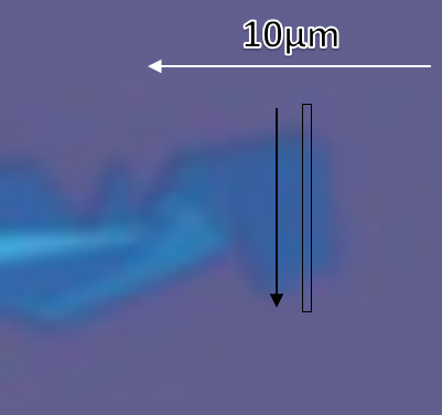
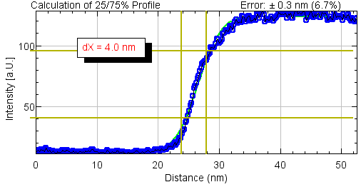
To measure the probe size, a helium ion image was acquired of a nearby high contrast edge on the sample surface shown in Figure S6. The probe size was measured to be 4.0 0.9 nm using the Gauss Fit plug-in in Imagej Rueden et al. (2017). It was assumed that the feature being imaged had a perfectly sharp edge. The decline in secondary electron intensity over the edge in the image is then attributed to the distribution of the ions in the probe Fox et al. (2015). This intensity profile was plotted and the distance between 25% and 75% of the average intensity of the flake was taken as the probe size. This is equivalent to the full width at half maximum of the probe.
VII Mass Loss
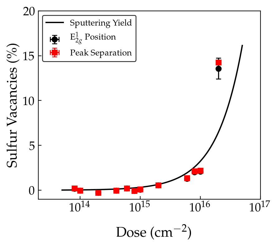
It has been previously reported that electron and ion irradiation of MoS2 can lead to the preferential sputtering of sulfur atoms Fox et al. (2015); Parkin et al. (2016). The resulting changes to the Raman spectrum were studied in detail by Parkin et al. in monolayer MoS2. We applied the assumption that the difference in changes to the peaks of 1L and 2L MoS2 would be negligible. We used their results to estimate the percentage of S atoms lost due to He+ irradiation in this work based on the shift of the peak and the increase in peak separation.
Figure S8 shows the missing sulfur percentage as a function of dose. The black markers are estimates from peak shift, the red are from peak separation changes and the line is from the sputtering yield in the two cited papers Maguire et al. (2018); Kretschmer et al. (2018).
The ion beam is expected to remove material with a preference for S atoms and S is heavier than any of the atmospheric species likely to fill its vacancies, decreasing with increasing dose. By comparison to literature Parkin et al. (2016) we see that changes to are small except at the highest doses and from the mass-adjusted LCM equation in the main paper those changes to are expected to cause a blue-shift, not red. Therefore we dismiss changes in as a cause for changing .
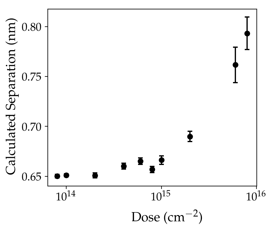
VIII Calculated Layer Separation
From the mass-adjusted LCM equation in the main paper we can calculate the increase in interlayer separation which would be required to explain the red shift if we exclude twisting and shear modulus effects. If the red shift of the shear mode was to be explained within the LCM by changes only to layer separation, then it would be calculated as follows:
| (S3) |
where is the interlayer separation, is the speed of light in cm s-1, is the shear modulus, is the single layer mass per unit area of pristine MoS2, is the sputter yield, , is the dose, is the atomic density, is the experimentally obtained change in the frequency of the shear mode, is the layer number (fixed at 2),
For direct comparison to our TEM experiment we calculate that for a dose of 61015 He+ cm-2, an increase in interlayer separation of 0.11 nm would be required. Since the results of this calculation do not agree with the TEM results presented in the main paper, we conclude that the change in layer separation is negligible and instead that twisting and shear modulus effects are responsible for the shift.
IX Twisting: Intensity and Frequency
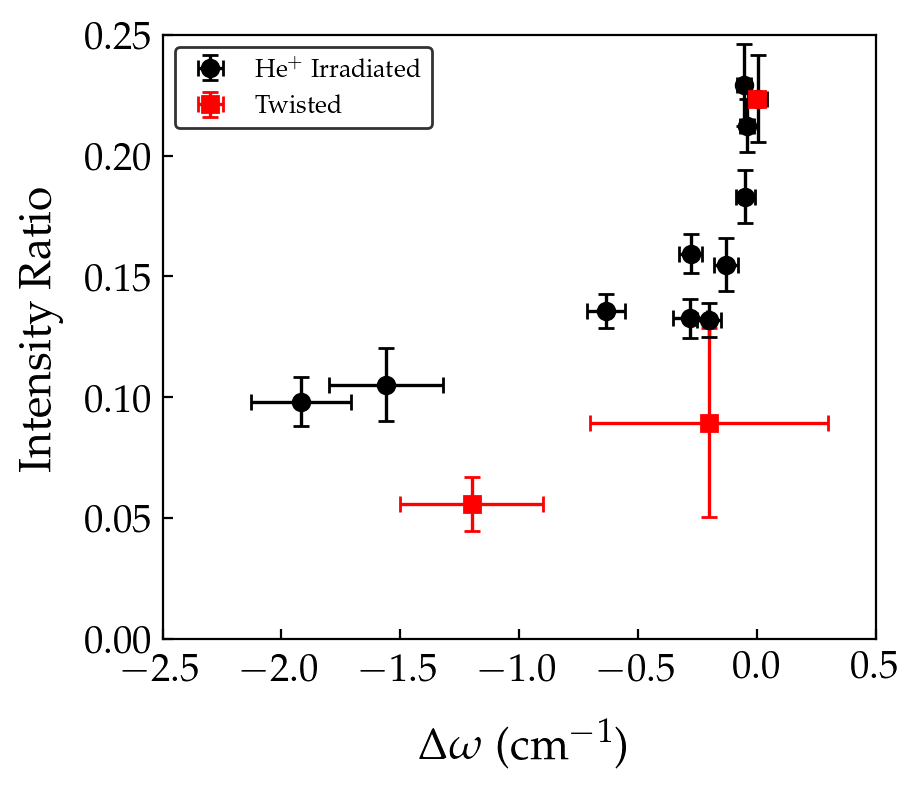
Figure S10 is a comparison of our data to that of Huang et al. Huang et al. (2016). Given the similarity, this figure shows that twisting is likely playing a large role in our irradiated material (particularly in explaining the loss of SM intensity) but orientation/twisting effects do not fully explain the red shift observed at a given value of the intensity ratio. Therefore, we suggest that reduced crystallinity causes a change in the shear modulus.
X Bibliography
References
- Novoselov et al. (2016) K. S. Novoselov, A. Mishchenko, A. Carvalho, and A. H. Castro Neto, Science 353, aac9439 (2016).
- Jariwala et al. (2016) D. Jariwala, T. J. Marks, and M. C. Hersam, Nature Materials 16, 170 (2016).
- Kang et al. (2017) K. Kang, K. H. Lee, Y. Han, H. Gao, S. Xie, D. A. Muller, and J. Park, Nature 550, 229 (2017).
- Sung et al. (2017) J. H. Sung, H. Heo, S. Si, Y. H. Kim, H. R. Noh, K. Song, J. Kim, C. S. Lee, S. Y. Seo, D. H. Kim, H. K. Kim, H. W. Yeom, T. H. Kim, S. Choi, J. S. Kim, and M. H. Jo, Nature Nanotechnology 12, 1064 (2017).
- Boukhicha et al. (2013) M. Boukhicha, M. Calandra, M. A. Measson, O. Lancry, and A. Shukla, Physical Review B 87, 1 (2013).
- Lui et al. (2015) C. H. Lui, Z. Ye, C. Ji, K. C. Chiu, C. T. Chou, T. I. Andersen, C. Means-Shively, H. Anderson, J. M. Wu, T. Kidd, Y. H. Lee, and R. He, Physical Review B 91, 1 (2015).
- Zhang et al. (2016) J. Zhang, J. Wang, P. Chen, Y. Sun, S. Wu, Z. Jia, X. Lu, H. Yu, W. Chen, J. Zhu, G. Xie, R. Yang, D. Shi, X. Xu, J. Xiang, K. Liu, and G. Zhang, Advanced Materials 28, 1950 (2016).
- Li et al. (2016) Y. Li, S. Lin, Y. S. Chui, and S. P. Lau, ECS Journal of Solid State Science and Technology 5, Q3033 (2016).
- Zhao et al. (2013) Y. Zhao, X. Luo, H. Li, J. Zhang, P. T. Araujo, C. K. Gan, J. Wu, H. Zhang, S. Y. Quek, M. S. Dresselhaus, and Q. Xiong, Nano Letters 13, 1007 (2013).
- Zhang et al. (2013) X. Zhang, W. P. Han, J. B. Wu, S. Milana, Y. Lu, Q. Q. Li, A. C. Ferrari, and P. H. Tan, Physical Review B 87, 115413 (2013).
- Zhang et al. (2015) X. Zhang, X. F. Qiao, W. Shi, J. B. Wu, D. S. Jiang, and P. H. Tan, Chem. Soc. Rev. 44, 2757 (2015).
- Lin et al. (2016) Z. Lin, B. R. Carvalho, E. Kahn, R. Lv, R. Rao, H. Terrones, M. A. Pimenta, and M. Terrones, 2D Materials 3 (2016).
- Song et al. (2016) Q. J. Song, Q. H. Tan, X. Zhang, J. B. Wu, B. W. Sheng, Y. Wan, X. Q. Wang, L. Dai, and P. H. Tan, Physical Review B 93, 115409 (2016).
- Lee et al. (2010) C. Lee, H. Yan, L. E. Brus, T. F. Heinz, J. Hone, and S. Ryu, ACS Nano 4, 2695 (2010).
- Li et al. (2012) H. Li, Q. Zhang, C. C. R. Yap, B. K. Tay, T. H. T. Edwin, A. Olivier, and D. Baillargeat, Advanced Functional Materials 22, 1385 (2012).
- O’Brien et al. (2015) M. O’Brien, N. McEvoy, D. Hanlon, T. Hallam, J. N. Coleman, and G. S. Duesberg, Scientific Reports 6, 1 (2015).
- Zeng et al. (2012) H. Zeng, B. Zhu, K. Liu, J. Fan, X. Cui, and Q. M. Zhang, Physical Review B 86, 1 (2012).
- Fox et al. (2015) D. S. Fox, Y. Zhou, P. Maguire, A. O’Neill, C. O’Coileáin, R. Gatensby, A. M. Glushenkov, T. Tao, G. S. Duesberg, I. V. Shvets, M. Abid, M. Abid, H. C. Wu, Y. Chen, J. N. Coleman, J. F. Donegan, and H. Zhang, Nano Letters 15, 5307 (2015).
- Ko et al. (2016) T. Y. Ko, A. Jeong, W. Kim, J. Lee, Y. Kim, J. E. Lee, G. H. Ryu, K. Park, D. Kim, Z. Lee, M. H. Lee, C. Lee, and S. Ryu, 2D Materials 4, 014003 (2016).
- Choudhary et al. (2016) N. Choudhary, M. R. Islam, N. Kang, L. Tetard, Y. Jung, and S. I. Khondaker, Journal of Physics Condensed Matter 28 (2016).
- Maguire et al. (2018) P. Maguire, D. S. Fox, Y. Zhou, Q. Wang, M. O. Brien, J. Jadwiszczak, C. P. Cullen, J. McManus, S. Bateman, N. Mcevoy, G. S. Duesberg, and H. Zhang, Physical Review B 98, 134109 (2018).
- Zhou et al. (2016) Y. Zhou, P. Maguire, J. Jadwiszczak, M. Muruganathan, H. Mizuta, and H. Zhang, Nanotechnology 27, 325302 (2016).
- Nanda et al. (2015) G. Nanda, S. Goswami, K. Watanabe, T. Taniguchi, and P. F. A. Alkemade, Nano Letters 15, 4006 (2015).
- Iberi et al. (2016) V. Iberi, L. Liangbo, A. V. Ievlev, M. G. Stanford, M. W. Lin, X. Li, M. Mahjouri-Samani, S. Jesse, B. G. Sumpter, S. V. Kalinin, D. C. Joy, K. Xiao, A. Belianinov, and O. S. Ovchinnikova, Scientific Reports 6 (2016).
- Stanford et al. (2016) M. G. Stanford, P. R. Pudasaini, A. Belianinov, N. Cross, J. H. Noh, M. R. Koehler, D. G. Mandrus, G. Duscher, A. J. Rondinone, I. N. Ivanov, T. Z. Ward, and P. D. Rack, Scientific Reports , 27276 (2016).
- Stanford et al. (2017) M. G. Stanford, P. R. Pudasaini, E. T. Gallmeier, N. Cross, L. Liang, A. Oyedele, G. Duscher, M. Mahjouri-Samani, K. Wang, K. Xiao, D. B. Geohegan, A. Belianinov, B. G. Sumpter, and P. D. Rack, Advanced Functional Materials 27 (2017).
- Nanda et al. (2017) G. Nanda, G. Hlawacek, S. Goswami, K. Watanabe, T. Taniguchi, and P. F. A. Alkemade, Carbon 119, 419 (2017).
- O’Brien et al. (2014) M. O’Brien, N. McEvoy, T. Hallam, H. Y. Kim, N. C. Berner, D. Hanlon, K. Lee, J. N. Coleman, and G. S. Duesberg, Scientific Reports 4, 7374 (2014).
- Castellanos-Gomez et al. (2012) A. Castellanos-Gomez, M. Barkelid, A. M. Goossens, V. E. Calado, H. S. J. Van Der Zant, and G. A. Steele, Nano Letters 12, 3187 (2012).
- Liang et al. (2017a) L. Liang, J. Zhang, B. G. Sumpter, Q. H. Tan, P. H. Tan, and V. Meunier, ACS Nano 11, 11777 (2017a).
- Liu et al. (2014) K. Liu, L. Zhang, T. Cao, C. Jin, D. Qiu, Q. Zhou, A. Zettle, P. Yang, S. G. Louie, and F. Wang, Nature Communications 5 (2014).
- Mignuzzi et al. (2015) S. Mignuzzi, A. J. Pollard, N. Bonini, B. Brennan, I. S. Gilmore, M. A. Pimenta, D. Richards, and D. Roy, Physical Review B 91, 195411 (2015).
- Klein et al. (2018) J. Klein, A. Kuc, A. Nolinder, M. Altzschner, J. Wierzbowski, F. Sigger, F. Kreupl, J. J. Finley, U. Wurstbauer, A. W. Holleitner, and M. Kaniber, 2D Materials 5, 011007 (2018).
- Splendiani et al. (2010) A. Splendiani, L. Sun, Y. Zhang, T. Li, J. Kim, C. Y. Chim, G. Galli, and F. Wang, Nano Letters 10, 1271 (2010).
- Scheuschner et al. (2014) N. Scheuschner, O. Ochedowski, A. M. Kaulitz, R. Gillen, M. Schleberger, and J. Maultzsch, Physical Review B 89, 125406 (2014).
- Tan et al. (2012) P. H. Tan, W. P. Han, W. J. Zhao, Z. H. Wu, K. Chang, H. Wang, Y. F. Wang, N. Bonini, N. Marzari, N. Pugno, G. Savini, A. Lombardo, and A. C. Ferrari, Nature Materials 11, 294 (2012).
- Kretschmer et al. (2018) S. Kretschmer, M. Maslov, S. Ghaderzadeh, M. Ghorbani-Asl, G. Hlawacek, and A. V. Krasheninnikov, ACS Applied Materials & Interfaces (2018).
- Parkin et al. (2016) W. M. Parkin, A. Balan, L. Liang, P. M. Das, M. Lamparski, C. H. Naylor, J. A. Rodríguez-Manzo, A. T. C. Johnson, V. Meunier, and M. Drndić, ACS Nano 10, 4134 (2016).
- Huang et al. (2016) S. Huang, L. Liang, X. Ling, A. A. Puretzky, D. B. Geohegan, B. G. Sumpter, J. Kong, V. Meunier, and M. S. Dresselhaus, Nano Letters 16, 1435 (2016).
- Liang et al. (2017b) L. Liang, A. A. Puretzky, B. G. Sumpter, and V. Meunier, Nanoscale 9, 15340 (2017b).
- Lahouij et al. (2012) I. Lahouij, B. Vacher, J. M. Martin, and F. Dassenoy, Wear 296, 558 (2012).
- Rueden et al. (2017) C. Rueden, J. Schindelin, M. Hiner, B. DeZonia, A. Walter, E. Arena, and K. Eliceiri, BMC Bioinformatics 18, 1 (2017).