Engineering chiral edge states in 2D topological insulator/ferromagnetic insulator heterostructures
Abstract
Chiral edge state (CES) at zero magnetic field has already been realized in the magnetically doped topological insulator (TI). However, this scheme strongly relies on material breakthroughs, and in fact, most of the TIs cannot be driven into a Chern insulator in this way. Here, we propose to achieve the CESs in 2D TI/ferromagnetic insulator/TI sandwiched structures through spin-selective coupling between the helical edge states of the two TIs. Due to this coupling, the edge states of one spin channel are gapped and those of the other spin channel remain almost gapless, so that the helical edge states of each isolated TI are changed into the CESs. Such CESs can be hopefully achieved in all TI materials, which are immune to magnetic-disorder-induced backscattering. We propose to implement our scheme in the van der Waals heterostructures between monolayer 1T’-WTe2 and bilayer CrI3. The electrical control of magnetism in bilayer CrI3 switches the transport direction of the CESs, which can realize a low-consumption transistor.
I introduction
The discovery of quantum Hall effect Klitzing et al. (1980) has lead to a revolution in condensed matter physics, that is, understanding phase transition in terms of band topology Thouless et al. (1982). Following this route, various topological materials have been found in the last decade, such as topological insulator (TI), superconductor, and semimetal Hasan and Kane (2010); Qi and Zhang (2011); Armitage et al. (2018). Apart from the significance in fundamental physics, the chiral edge states (CESs) in quantum Hall phase also has important applications in both quantum information processing and dissipationless electron transport Qi and Zhang (2011). The unidirectional channel of the CESs avoids all kinds of elastic backscattering, resulting in a long phase coherence length Ji et al. (2003); Henny et al. (1999); Neder et al. (2007) and a low energy dissipation.
The quantum Hall effect is stabilized by a strong magnetic field, which is inapplicable for a low-consumption integrated circuit in the future. Therefore, searching for CESs without magnetic field is of great interest. Quantum Hall effect without external magnetic field is called quantum anomalous Hall effect, or Chern insulator, which was first proposed by Haldane Haldane (1988). Recently, the quantum anomalous Hall effect has been realized in thin films of chromium-doped (Bi,Sb)2Te3, a magnetically doped TI Chang et al. (2013); Yu et al. (2010). The spontaneous ferromagnetic order in the TI breaks time-reversal symmetry, results in a nonzero Chern number. Accordingly, the helical edge states in the TI are turned into the chiral ones Liu et al. (2008); Klinovaja and Loss (2015), the latter being more robust due to the lack of backscattering channels Li et al. (2013). Although the physical scenario of engineering Chern insulator by magnetically doping a TI is general, its realization strongly relies on the details of the bulk material. In fact, due to the complex interaction between electrons and magnetic impurities, in most of the cases, a ferromagnetic order cannot be established in the TI materials. For example, in HgMnTe, magnetic moments do not order spontaneously and an additional small Zeeman field is required Yu et al. (2010); Liu et al. (2008). This brings up an interesting question that whether or not there is a general way to create CESs which does not rely too much on specific properties of the bulk material used.
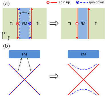
In this work, we propose to engineer CESs in a 2D TI/ferromagnetic insulator (FI)/TI sandwiched structure, which can be hopefully applied to all 2D TI materials. The Zeeman splitting inside the FI introduces a spin-selective coupling between two adjacent helical edge states of two TIs as shown in Fig. 1. As a result of this coupling, the spin-down edge states are gapped but the spin-up ones remain almost gapless, so that the helical edge states of each isolated TI are changed into the CESs. The scenario here is quite different from the magnetically doping method. For the present sandwiched structure, there is no topological phase transition in the bulk state, and its CESs are not protected by the bulk band topology. However, such CESs share all the properties of that in the Chern insulator. Due to the lack of the backscattering channel, they are very robust against magnetic disorder and favorable to dissipationless directed transport. We propose to implement our scheme in the van der Waals heterostructures between monolayer 1T’-WTe2 and bilayer CrI3. The magnetism in bilayer CrI3 can be controlled by electronic field, which can switch the transport direction of the CESs, providing an important application of a low-consumption transistor.
The rest of this paper is organized as follows. In Sec. II, we apply a perturbation approach to the low-energy model of the TI to show the basic mechanism of our scheme. The perturbation result is further verified by numerical calculations based on a lattice model in Sec. III. In order to show the robustness of the CESs, we calculate conductance in the presence of magnetic disorder in Sec. IV. The experimental realization of our proposal and possible application of the low-consumption transistor are discussed in Sec. V. Finally, a brief summary is given in Sec. VI.
II basic physical picture
The main idea of the CESs engineering is sketched in Fig. 1 in a TI/FI/TI junction, where an FI film is sandwiched between two TIs along the direction. The whole Hamiltonian of this system can be written as
| (1) |
Here is the the low-energy effective Hamiltonian describing the helical edge states of the two TIs, yielding
| (2) |
where is the velocity of electrons in the edge channels, and momentum is along the direction, as seen in Fig. 1(a). is the Fermi operator with spin subscripts and edge ones , where () denote the left (right) TIs. The Pauli matrices and operate in spin and left/right TIs, respectively. The energy spectrum is given by , which is measured from the Dirac point at . is the Hamiltonian of the middle FI, which can be described by
| (3) |
where is the Fermi operator in the FI, , and is the energy difference between the spin- band bottom and the Dirac point. The spin dependence of arises from the Zeeman spin splitting in the FI. Without loss of generality, it is assumed that for the spin-up electrons is much larger than for the spin-down electrons. Moreover, we confine the present study to a single transverse mode in the FI. It is straightforward to extend the result obtained to the multiple channel case. The coupling between the FI and the helical edge states of the TI can be captured by
| (4) |
where is the coupling strength between the helical edge states and the states inside the FI. Usually, is very small compared with , i.e., . Taking this fact into account, we treat the term as a perturbation to of the decoupled system.
The coupling between the helical edge states and the FI induces a spin-selective gap opening in the edge states, which can be obtained by solving the effective model of Eq. (1). Note that the spin component is conserved for the whole system so that the edge states for each spin polarization can be solved independently. We formally write down the Schrödinger equation for the spin- electrons as
| (5) |
where , and , which can be read from Eq. (1), and wave functions and refer to the spin- edge states of the two TIs and the bulk states in the FI, respectively. By eliminating in the two equations above, we obtain the equation for the edge states as
| (6) |
where is the self-energy with as the bare Green’s function of the FI. The self-energy can be solved directly as , where is the identity matrix in the left/right TI space. We focus on the parametric region around the Dirac point at which and . Then the self-energy reduces to with . The effective Hamiltonian for the modified edge states now becomes
| (7) |
Correspondingly, the energy spectrum is given by
| (8) |
One can see that a gap with size appears at , and the band is shifted by as well. The physical reason is that the hybridization between TIs and FI introduces an indirect coupling between edge states in the two TIs and so opens a gap. The coupling is independent of spin, and spin-dependent gap is determined by . For , corresponding to a strong spin splitting in the FI, we have . In this case, only the spin-down edge states are gapped, while the spin-up edge states remain almost gapless, thus forming CESs, as shown in Fig. 1(b).
From the above perturbation approach, we have seen that the spin-selective coupling between the two TIs can drive the original helical edge states into the CESs. In the following, we will perform numerical calculation to verify this conclusion.
III lattice model simulation
We adopt the Bernevig-Hughes-Zhang (BHZ) model Bernevig et al. (2006) of the HgTe/CdTe quantum wells to describe the 2D TI. It is expected that the main results do not rely on the specific model, for the picture based on the edge states in Sec. II holds generally, independent of specific TI materials. The BHZ model takes the following form Bernevig et al. (2006); König et al. (2008)
| (9) |
where are the Pauli matrices operating on the and orbital degrees of freedom, and . and are the relevant material parameters, which can be experimentally controlled. In the long wavelength limit, the BHZ model can be mapped onto a square lattice by discretizing the continuous model in Eq. (9). By the substitution of , , and , we obtain the tight-binding Hamiltonian as
| (10) | |||||
where is the Fermi operator on site with both orbital and spin components. is the index of the discrete sites in the square lattice, and are the unit vectors along the and directions, respectively, with as the lattice constant. and are 44 block matrices and take the explicit form
| (11) |
The band inversion of the HgTe/CdTe quantum wells occurs at a critical thickness nm. Here we take the physical parameters for the system with a thickness of nm König et al. (2008): nm meV, nm2 meV, nm2 meV, and meV. The lattice constant is set to nm.
The tight-binding model for the FI can be obtained in a similar way, yielding
| (12) |
where denotes the spinful fermion operator in the FI, includes chemical potential and Zeeman splitting , and is the nearest neighbour hopping. The parameters for the FI are set to nm2 meV, meV, and meV. Due to the Zeeman exchange field, the spin-up and spin-down bands split. In the following, we adopt multiple bands with slight splitting for the FI to simulate a reasonable bulk density of states.
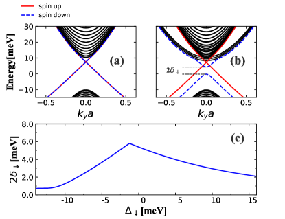
The whole hybridized system has a strip geometry along the direction, see Fig. 1(a). Since we are only interested in the edge states at the TI/FI interfaces, in the numerical calculation, the outer boundaries of two TIs are assumed to connected with each other by the same hopping strength as in the bulk TI. Therefore, the system is equivalent to a cylinder. The band structure is calculated using the Kwant program Groth et al. (2014a), and the calculated result is shown in Fig. 2. In the absence of interface coupling between the TIs and FI, two TIs are isolated, and each one contains a pair of gapless helical states at the interface, see Fig. 2(a). As the interface hopping is turned on with a strength of nm2 meV, a large energy gap is induced for the spin-down channel, but the spin-up channel remains almost decoupled and gapless, as seen in Fig. 2(b). These results are in good agreement with the analytic result obtained in Sec. II. In addition of the gap opening, the band is shifted in Fig. 2(b), which was also predicted in the analytic result above. We also investigate the effect of the chemical potential in the FI. Tuning results in a change of the energy gap in the FI. The induced gap of the spin-down edge states as a function of is shown in Fig, 2(c). For a large , they are approximately related by based on the perturbation result in Sec. II. However, as decreases to a small value, decays as well, because in that case the minimal gap for the CESs is determined by in the FI. It should be noted that for real materials, more effects of magnetic proximity should be taken into consideration, including the redistribution of charge and spin at the interface, and band bending effect, etc. Eremeev et al. (2013); Men’shov et al. (2013); Eremeev et al. (2015).
IV conductance calculation
In the 2D TIs, the helical edge states are protected by time-reversal symmetry, which can be regarded as two copies of CESs forming a Kramers pair Kane and Mele (2005). For impurity potential that obeys time-reversal symmetry, helical electrons cannot be backscattered in the absence of interactions Xu and Moore (2006), because any backscattering requires a spin flipping due to the spin-momentum locking. However, a static magnetic impurity can induce spin-flip backscattering in the helical edge states and lead to a suppression of the conductance Qi and Zhang (2011). In the 2D TIs, perfect quantization of the edge conductance has not been achieved so far König et al. (2007); Roth et al. (2009); Knez et al. (2014); Du et al. (2015); Wu et al. (2018), in contrast to the high-quality quantum Hall plateaus Klitzing et al. (1980); Chang et al. (2013). The CESs are very robust against impurity and disorder, no matter whether they are magnetic or non-magnetic, because of the absence of backscattering channel. In what follows we numerically investigate the effects of magnetic disorder on the conductance in both helical and chiral edge states. It is expected that the CESs achieved by band engineering in Fig. 1 are more robust against magnetic disorder, resulting in dissipationless transport.
The lattice model of the system is the same as that in Sec. III. In addition, we add magnetic disorder to the whole system, whose Hamiltonion is given by
| (13) |
where are the random on-site spin flipping. We adopt an uncorrelated Gaussian distribution of with strength . The transport occurs along the direction and the differential conductance is calculated using the KWANT program Groth et al. (2014b).
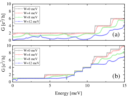
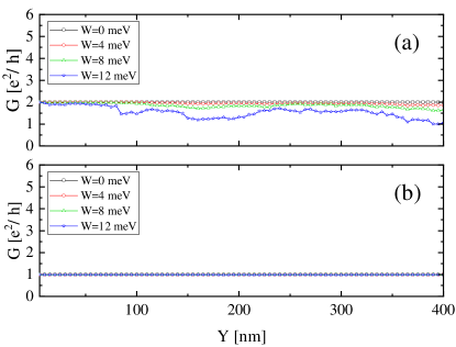
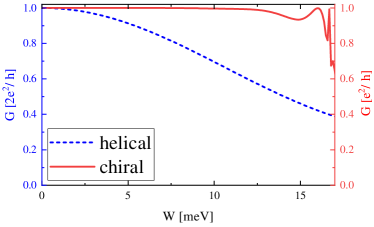
We compare the calculated conductances of the chiral and helical edge states in Figs. 3 and 4, which can be achieved by turning on and off the interface hopping between TIs and FI in the calculation. Figure 3 shows the conductance as a function of incident energy for different strengths of magnetic disorder. Without disorder, the helical and chiral edge channels show quantized conductances and , respectively. The lowest plateau is contributed by the edge states. For the helical edge states in Fig. 3(a), the conductance is sensitive to the magnetic disorder. For meV, the conductance is strongly suppressed. In contrast, the effect of magnetic disorder on the CESs is much weaker, and the conductance remains quantized within the energy gap induced by the spin-selective coupling [cf. Fig. 2(b)]. The inter-edge reflection (between two TIs) of the CESs induced by magnetic impurities through virtual scattering between different spin states can be evaluated as , where is the spatial overlap between the spin-up and spin-down edge states. Since the spin-down states in the two TIs penetrate into the FI and couple with each other while the spin-up states are still well localized, the overlap of their wave functions is small, indicating a weak backscattering Li et al. (2013). For a fixed incident energy, the conductance as a function of the length of the disordered region in the direction is shown in Fig. 4. Similar to the results in Fig. 3, in the presence of magnetic disorder, the conductance for the helical edge states decreases with the length of the system, indicating a strong dissipation induced by the magnetic disorder. However, the quantized conductance through the CESs retains with increasing size of the system. We further compare the dependence of edge conductance on disorder strength in Fig. 5. One can see that the conductance of helical edge states decrease much faster than that of the CESs, which shows the robustness of the CESs via band engineering. Up to the disorder strength meV, which is much larger than the energy gap of the CESs, the transport of the CESs is always dissipationless.
V experimental realization
We would like to discuss the experimental realization of our proposal. The building blocks for the CESs in our proposal are the 2D TI and FI. Many materials of TI have been reported Ando (2013), such as quantum wells König et al. (2007); Roth et al. (2009); Knez et al. (2014); Du et al. (2015), the thin film of 3D TIs Liu et al. (2010) and recently discovered single-layer transition metal dichalcogenides Qian et al. (2014); Wu et al. (2018); Peng et al. (2017); Tang et al. (2017). Moreover, the TI/FI heterostructures have also been synthesized Fan et al. (2014); Kou et al. (2013); Mellnik et al. (2014); Wang et al. (2016); Fan et al. (2016); Baker et al. (2015), so that our proposal can be hopefully realized by using the state-of-the-art technique in this research field. In order to achieve the CES engineering, there are several conditions to be fulfilled. First, the FI needs to be an insulator, otherwise the edge states will merge into the bulk states in the FI. Second, to achieve a spin-selective coupling between the helical edge states, one of the spin states needs to penetrate into the FI region. Therefore, the energy difference between the band bottom of the FI and the Dirac point in the helical edge states should have a proper value, and the width of the FI in the direction should be comparable with the spreading of the edge states. Third, a big Zeeman filed is favorable for the band engineering, which guarantees a negligible coupling for the edge states with opposite spins.
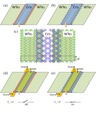
Recent progress on the 2D van der Waals crystals has shown that both TI and FI can be achieved in monolayer or bilayer crystals Qian et al. (2014); Wu et al. (2018); Peng et al. (2017); Tang et al. (2017); Gong et al. (2017); Huang et al. (2017); Samarth (2017); Huang et al. (2018). The benefit of these materials is that they can be reassembled into designer heterostructures made layer by layer in a precisely chosen sequence Geim and Grigorieva (2013). Moreover, the physical parameters in such 2D materials can be easily tuned by gate voltage, such as the chemical potential and even magnetism Huang et al. (2018). Thus these materials open a new avenue to realize our proposal in the van der Waals heterostructures. We propose to use monolayer 1T’-WTe2 as a TI Qian et al. (2014); Wu et al. (2018); Peng et al. (2017); Tang et al. (2017) and the bilayer CrI3 as an FI Huang et al. (2018) to synthesize the heterostructures, see Fig. 6. Based on the lattice parameters for both materials Zheng et al. (2016); McGuire et al. (2015), the monolayer 1T’-WTe2 and bilayer CrI3 lattices can match very well along the -direction as shown in Fig. 6(c). The helical edge states can be obtained in the 1T’-WTe2 nanoribbon periodic along the -direction Zheng et al. (2016), which can serve as a good candidate for the CESs engineering. 1T’-WTe2 has a large topological gap eV Qian et al. (2014) which results in the quantum spin Hall effect up to 100 K Wu et al. (2018). The large bulk gap of the TI can also support a large gap opening in the CESs (Fig. 2), since the gap opening in the edge states is limited by the bulk gap of the TI. The advantage of CrI3 is that its magnetism can be electrically controlled Huang et al. (2018), which means that the intrinsic Zeeman field can be tuned by an electric gate Matsukura et al. (2015). This remarkable effect opens the possibility to achieve a low-consumption transistor based on the electrically tunable CESs, see Figs. 6(d), 6(e). The direction of the ferromagnetic order in the FI is controlled by gate voltage and then it determines the spin and transport direction of the CESs. For example, when there is no CESs flows from the source to the drain so that the transistor is turned off [Fig. 6(d)]. Oppositely, when the CESs flow in the opposite direction and the transistor is turned on [Fig. 6(e)]. The robustness of the CESs guarantees a very low power dissipation and strongly suppresses the heat generation. By stacking multiple layers of the system, which is the main advantage of the van der Waals heterostructures, the on/off ratio of the transistor can be enhanced Qian et al. (2014); Liu et al. (2014). As a result, a dissipationless transistor based on the CESs engineering can be hopefully implemented.
VI summary
To summarize, we have shown that CESs can be engineered in the TI/FI/TI junction. The middle FI film can introduce a spin-selective coupling between the helical edge states in the TIs and so open a gap in the edge states of one spin channel. The edge states of the other spin channel remain almost gapless, and the resulting CESs are much more robust against magnetic disorder than the helical edge states. We proposed to implement such CESs in the van der Waals heterostructures of monolayer 1T’-WTe2 and bilayer CrI3. The recently achieved electric control of magnetism in bilayer CrI3 indicates that a CESs based low-consumption transistor can be realized by our proposal.
Acknowledgements.
We thank J. L. Lado, O. Zilberberg and Yong-Ping Du for helpful discussions. W. C. acknowledges the support from the National Natural Science Foundation of China under Grants No. 11504171. D. Y. X. acknowledges the support from the State Key Program for Basic Researches of China under Grants No. 2017YFA0303203.References
- Klitzing et al. (1980) K. v. Klitzing, G. Dorda, and M. Pepper, Physical Review Letters 45, 494 (1980).
- Thouless et al. (1982) D. J. Thouless, M. Kohmoto, M. P. Nightingale, and M. den Nijs, Physical Review Letters 49, 405 (1982).
- Hasan and Kane (2010) M. Z. Hasan and C. L. Kane, Rev. Mod. Phys. 82, 3045 (2010).
- Qi and Zhang (2011) X.-L. Qi and S.-C. Zhang, Rev. Mod. Phys. 83, 1057 (2011).
- Armitage et al. (2018) N. P. Armitage, E. J. Mele, and A. Vishwanath, Rev. Mod. Phys. 90, 015001 (2018).
- Ji et al. (2003) Y. Ji, Y. Chung, D. Sprinzak, M. Heiblum, D. Mahalu, and H. Shtrikman, Nature 422, 415 (2003).
- Henny et al. (1999) M. Henny, S. Oberholzer, C. Strunk, T. Heinzel, K. Ensslin, M. Holland, and C. Schönenberger, Science 284, 296 (1999).
- Neder et al. (2007) I. Neder, N. Ofek, Y. Chung, M. Heiblum, D. Mahalu, and V. Umansky, Nature 448, 333 (2007).
- Haldane (1988) F. D. M. Haldane, Phys. Rev. Lett. 61, 2015 (1988).
- Chang et al. (2013) C.-Z. Chang, J. Zhang, X. Feng, J. Shen, Z. Zhang, M. Guo, K. Li, Y. Ou, P. Wei, L.-L. Wang, Z.-Q. Ji, Y. Feng, S. Ji, X. Chen, J. Jia, X. Dai, Z. Fang, S.-C. Zhang, K. He, Y. Wang, L. Lu, X.-C. Ma, and Q.-K. Xue, Science 340, 167 (2013).
- Yu et al. (2010) R. Yu, W. Zhang, H.-J. Zhang, S.-C. Zhang, X. Dai, and Z. Fang, Science 329, 61 (2010).
- Liu et al. (2008) C.-X. Liu, X.-L. Qi, X. Dai, Z. Fang, and S.-C. Zhang, Phys. Rev. Lett. 101, 146802 (2008).
- Klinovaja and Loss (2015) J. Klinovaja and D. Loss, Phys. Rev. B 92, 121410 (2015).
- Li et al. (2013) H. Li, L. Sheng, R. Shen, L. B. Shao, B. Wang, D. N. Sheng, and D. Y. Xing, Phys. Rev. Lett. 110, 266802 (2013).
- Bernevig et al. (2006) B. A. Bernevig, T. L. Hughes, and S.-C. Zhang, Science 314, 1757 (2006).
- König et al. (2008) M. König, H. Buhmann, L. W. Molenkamp, T. Hughes, C.-X. Liu, X.-L. Qi, and S.-C. Zhang, Journal of the Physical Society of Japan 77, 031007 (2008).
- Groth et al. (2014a) C. W. Groth, M. Wimmer, A. R. Akhmerov, and X. Waintal, New Journal of Physics 16, 063065 (2014a).
- Eremeev et al. (2013) S. V. Eremeev, V. N. Men’shov, V. V. Tugushev, P. M. Echenique, and E. V. Chulkov, Phys. Rev. B 88, 144430 (2013).
- Men’shov et al. (2013) V. N. Men’shov, V. V. Tugushev, S. V. Eremeev, P. M. Echenique, and E. V. Chulkov, Phys. Rev. B 88, 224401 (2013).
- Eremeev et al. (2015) S. Eremeev, V. Men, V. Tugushev, E. V. Chulkov, et al., Journal of Magnetism and Magnetic Materials 383, 30 (2015).
- Kane and Mele (2005) C. L. Kane and E. J. Mele, Phys. Rev. Lett. 95, 226801 (2005).
- Xu and Moore (2006) C. Xu and J. E. Moore, Phys. Rev. B 73, 045322 (2006).
- König et al. (2007) M. König, S. Wiedmann, C. Brüne, A. Roth, H. Buhmann, L. W. Molenkamp, X.-L. Qi, and S.-C. Zhang, Science 318, 766 (2007), http://science.sciencemag.org/content/318/5851/766.full.pdf .
- Roth et al. (2009) A. Roth, C. Brüne, H. Buhmann, L. W. Molenkamp, J. Maciejko, X.-L. Qi, and S.-C. Zhang, Science 325, 294 (2009), http://science.sciencemag.org/content/325/5938/294.full.pdf .
- Knez et al. (2014) I. Knez, C. T. Rettner, S.-H. Yang, S. S. P. Parkin, L. Du, R.-R. Du, and G. Sullivan, Phys. Rev. Lett. 112, 026602 (2014).
- Du et al. (2015) L. Du, I. Knez, G. Sullivan, and R.-R. Du, Phys. Rev. Lett. 114, 096802 (2015).
- Wu et al. (2018) S. Wu, V. Fatemi, Q. D. Gibson, K. Watanabe, T. Taniguchi, R. J. Cava, and P. Jarillo-Herrero, Science 359, 76 (2018).
- Groth et al. (2014b) C. W. Groth, M. Wimmer, A. R. Akhmerov, and X. Waintal, New Journal of Physics 16, 063065 (2014b).
- Ando (2013) Y. Ando, Journal of the Physical Society of Japan 82, 102001 (2013).
- Liu et al. (2010) C.-X. Liu, H. Zhang, B. Yan, X.-L. Qi, T. Frauenheim, X. Dai, Z. Fang, and S.-C. Zhang, Phys. Rev. B 81, 041307 (2010).
- Qian et al. (2014) X. Qian, J. Liu, L. Fu, and J. Li, Science , 1256815 (2014).
- Peng et al. (2017) L. Peng, Y. Yuan, G. Li, X. Yang, J.-J. Xian, C.-J. Yi, Y.-G. Shi, and Y.-S. Fu, Nature communications 8, 659 (2017).
- Tang et al. (2017) S. Tang, C. Zhang, D. Wong, Z. Pedramrazi, H.-Z. Tsai, C. Jia, B. Moritz, M. Claassen, H. Ryu, S. Kahn, et al., Nature Physics 13, 683 (2017).
- Fan et al. (2014) Y. Fan, P. Upadhyaya, X. Kou, M. Lang, S. Takei, Z. Wang, J. Tang, L. He, L.-T. Chang, M. Montazeri, et al., Nature materials 13, 699 (2014).
- Kou et al. (2013) X. Kou, L. He, M. Lang, Y. Fan, K. Wong, Y. Jiang, T. Nie, W. Jiang, P. Upadhyaya, Z. Xing, et al., Nano letters 13, 4587 (2013).
- Mellnik et al. (2014) A. R. Mellnik, J. S. Lee, A. Richardella, J. L. Grab, P. J. Mintun, M. H. Fischer, A. Vaezi, A. Manchon, E.-A. Kim, N. Samarth, and D. C. Ralph, Nature 511, 449 (2014), letter.
- Wang et al. (2016) H. Wang, J. Kally, J. S. Lee, T. Liu, H. Chang, D. R. Hickey, K. A. Mkhoyan, M. Wu, A. Richardella, and N. Samarth, Phys. Rev. Lett. 117, 076601 (2016).
- Fan et al. (2016) Y. Fan, X. Kou, P. Upadhyaya, Q. Shao, L. Pan, M. Lang, X. Che, J. Tang, M. Montazeri, K. Murata, et al., Nature nanotechnology 11, 352 (2016).
- Baker et al. (2015) A. Baker, A. Figueroa, L. Collins-McIntyre, G. Van Der Laan, and T. Hesjedal, Scientific Reports 5, 7907 (2015).
- Gong et al. (2017) C. Gong, L. Li, Z. Li, H. Ji, A. Stern, Y. Xia, T. Cao, W. Bao, C. Wang, Y. Wang, et al., Nature 546, 265 (2017).
- Huang et al. (2017) B. Huang, G. Clark, E. Navarro-Moratalla, D. R. Klein, R. Cheng, K. L. Seyler, D. Zhong, E. Schmidgall, M. A. McGuire, D. H. Cobden, et al., Nature 546, 270 (2017).
- Samarth (2017) N. Samarth, Nature 546, 216 (2017).
- Huang et al. (2018) B. Huang, G. Clark, D. R. Klein, D. MacNeill, E. Navarro-Moratalla, K. L. Seyler, N. Wilson, M. A. McGuire, D. H. Cobden, D. Xiao, et al., Nature nanotechnology , 1 (2018).
- Geim and Grigorieva (2013) A. K. Geim and I. V. Grigorieva, Nature 499, 419 (2013).
- Zheng et al. (2016) F. Zheng, C. Cai, S. Ge, X. Zhang, X. Liu, H. Lu, Y. Zhang, J. Qiu, T. Taniguchi, K. Watanabe, et al., Advanced Materials 28, 4845 (2016).
- McGuire et al. (2015) M. A. McGuire, H. Dixit, V. R. Cooper, and B. C. Sales, Chemistry of Materials 27, 612 (2015).
- Matsukura et al. (2015) F. Matsukura, Y. Tokura, and H. Ohno, Nature nanotechnology 10, 209 (2015).
- Liu et al. (2014) J. Liu, T. H. Hsieh, P. Wei, W. Duan, J. Moodera, and L. Fu, Nature materials 13, 178 (2014).