Spin-Splitting and Rashba-Effect at Mono-Layer GaTe in the Presence of Strain
Abstract
In this paper, spintronic properties of a mono-layer GaTe under biaxial and uniaxial strain is investigated. Here, spin properties of two structures of GaTe, one with mirror symmetry and the other with inversion symmetry, is studied. We have also calculated the band structure of GaTe with and without spin-orbit coupling to find out the importance of spin–orbit interaction (SOI) on its band structure. We find band gap can be modified by applying spin-orbit coupling in the presence of strain. We explore Mexican-hat dispersion for different structures and different strain. We find Mexican-hat can be tuned by strain however some cases shows any Mexican-hat. We calculate spin-splitting in conduction and valence band in the presence of strain where the structure with inversion symmetry doesn’t show any splitting. We find in some cases, GaTe indicates Rashba dispersion that can be adjusted by strain. The amount of Rashba parameters may be in the order of other reported two-dimensional materials.
I introduction
Two-dimensional materials have attracted a great attention in the past decade due to their fascinating physical and chemical properties. These excellent properties can result in device applications. 2D layered materials such as Graphene and transition metal di-chalcogenides and others two-dimensional material, can be separated simply by mechanical or liquid-phase exfoliation from their bulk layered solids, which a mono-layer can be exfoliated by the weak interlayer van der Waals (vdW) forces. These mono-layer materials studied extensively for wide range of applications in Field-effect transistors, spintronic devices. Novoselov et al. (2004); Wang et al. (2014); Huang et al. (2016); Guo et al. (2015); Fei and Yang (2014). Nevertheless, the lack of an intrinsic band gap or high band gap has encountered with problem for application in electronic and optoelectronic devices Li et al. (2012); Elias et al. (2009); Ma et al. (2012); Zhou et al. (2009).
In which case, the search for new 2D materials that may introduce new properties for specific applications is of technological requirements. Bulk MX(M=Ga,In and X=S, Se,Te) consist of several mono-layers per unit cell weakly bonded by van der Waals forces and form different crystal phases (e.g., and -type) depending on the layer stacking sequence.
These class of two-dimensional materials has been extensively studied for potential applications in photo-detectors, gas sensors and optoelectronic devices Koppens et al. (2014); Hu et al. (2014); Rao et al. (2015). In these material class, GaTe has a special place among the members of the III-VI family, since Ga and Te are massive atoms in which spin orbit coupling is stronger than the others. In order to become suitable for different applications, the corrections of its intrinsic properties is required. For example, a broad range of chemical methods Şahin and Ciraci (2011) and doping methodsSheng et al. (2012) have been studied to tune the band gap of GaTe. Gallium telluride (GaTe), can be an ideal candidate for using strain engineering as an effective method to change their electronic and spin properties. It has been proved that the band gap of GaTe can be controlled by applying strain both experimentallyCocco et al. (2010) and theoreticallyGui et al. (2008).
Mexican hat dispersion in this class have been studied and It has been studied that a Mexican-hat-shaped dispersion observed at the valence band maximum (VBM) in monolayer of GaTe. This dispersion in the band structure lead to van Hove singularity in the density of states (DOS). Mexican hat dispersion provides 1D-like electronic density of states of the valence band near the band edge Rybkovskiy et al. (2014). The effects of this singularity on the magnetic and electronic properties has been studied Wickramaratne et al. (2014); Cao et al. (2015); Zólyomi et al. (2013); Wu et al. (2014); Magorrian et al. (2016); Rybkovskiy et al. (2014). However, this sharp van Hove singularity near the Fermi level could induce a spin splitting in the band structure and suitable magnetismCao et al. (2015); Wu et al. (2014). One can observe Lifshitz phase transition due to this sharp van Hove singularity Lifshitz et al. (1960).The high density of states at the valence band edge, in principle, is beneficial to high thermoelectric power factor in this material Wickramaratne et al. (2015).
Spin-orbit-induced spin splitting and spin-orbit interaction (SOI) is believed be responsible of Spin relaxation mechanisms in 2D materials. Dat T. Do et.al. Do et al. (2015) studied spin-splitting in 2D mono chalcogenides. They considered GaTe in monoclinic structure and reported zero spin splitting because it has inversion symmetry at mono-layer.
Here, we study two different phases of GaTe and observe spin splitting in one phase and other phase exhibits any spin-splitting due to the inversion symmetry. Spin-splitting can be tuned by tensile and compressive strain. Rashba effect also observed in compressive regime. Rashba spin-orbit interaction originates from the lack of inversion symmetry Bychkov and Rashba (1984).
The Rashba effect has been studied intensively in the spintronics since it can be used to tune the spin direction by means of an electric field and applicable in spin-field effect transistor Datta and Das (1990). Experimentally, Rashba effect has been reported experimentally in quantum wells , surfaces of heavy metals, and BiTeI and theoretical for two-dimensional materials, for instance graphene, polar transition-metal dichalcogenide monolayers Absor et al. (2018a), the MoS2 /Bi(111) heterostructure, GaX(mono-chalcogenides)/TMDC heterostructures Zhang and Schwingenschlögl (2018), and gated multilayer InSe Premasiri et al. (2018). Spin properties is the focus of the present study Nitta et al. (1997); LaShell (1996); Žutić (2004); Kimura et al. (2010); Konschuh et al. (2010); Cheng et al. (2013); Liu et al. (2013); Min et al. (2006); Ishizaka (2011); Ast et al. (2007); Koroteev et al. (2004); Lee et al. (2015).
In spintronics and optoelectronics have stimulated the research for materials capable of presenting a great degree of spin polarization and long spin relaxation time Žutić et al. (2004). If symmetry is broken by strain, quantum phase transitions such as semiconductor-semimetal transition are possible Zhang et al. (2015).
In this work we discuss the magnetic and electronic properties of monolayer crystals of GaTe. We present the electronic band structures and spin-splitting for monolayer Gallium telluride applying by biaxial and uniaxial in-plane strain.
II Computational details
The analysis of monolayer GaTe was carried out using density-functional theory (DFT) as implemented in the Quantum Espresso Giannozzi et al. (2009, 2017) plane-wave-basis codes using projector augmented wave (PAW) Blöchl (1994); Kresse and Joubert (1999). To calculate the geometries and band-structures, we used semilocal exchange-correlation functional functional with high-throughput ultrasoft pseudopotential: PBEsol Perdew et al. (2008). The plane-wave cutoff energy was 612 eV. During calculation, a Monkhorst-Pack k-point grid was used for electrical properties but a denser k-mesh should be used for Rashba calculations, here we used a k-point mesh. We were first performed full geometry optimization until the forces on the atoms are less than 0.01 .
We explore two phases and of GaTe monolayer which these two phases was shown in the Fig. 1. phase with group symmetry forms a 2D honeycomb structure, which vertically placed Ga and Te pairs at two different sub-lattices. The structure of with phase can be observed in of Fig. 1(b), that one of the Te layer shifted with respect to the other. This phase breaks the mirror symmetry of the original structure but forms inversion symmetry.
Biaxial and uniaxial strain is applied for each phases and geometry is completely relaxed for two phases. Total energy and lattice constant for two phases is the same. Band structure with and without spin-orbit coupling is studied electronic and spintronic properties is investigated.
III Results and discussion
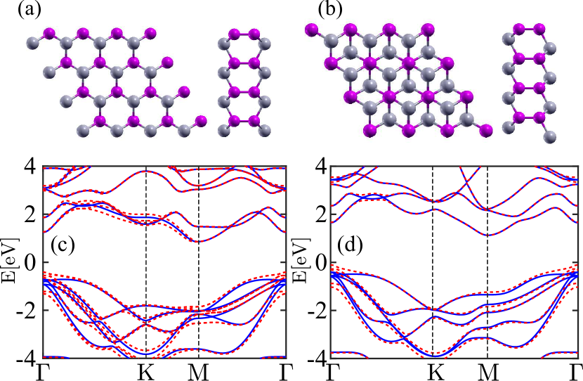
The calculated electronic band structures for two phases are plotted in the Fig. 1. Two phases are indirect-gap semiconductors, primarily due to the valence-band maximum (VBM) move from the point and the conduction-band minimum (CBM) located at the point. The band-gap in the phase is . The indirect band gap in phase is in agreement with the DFT results Ge et al. (2017); Cai et al. (2016a, b); Huang et al. (2015); Zhuang and Hennig (2013) for monolayer GaTe. Although, we calculated the electronic properties of GaTe with the spin-orbit coupling which Fig. 1 indicates SOC changes the band structure and then in this regime, band-gap declines to . SOC consideration causes to band-gap deceases by about . Spin-orbit interaction also moves the valence-band maximum to point and removes Mexican-hat dispersion.
phase of GaTe is the other structure, that can be distinguished by comparing optically active [infrared (IR) and Raman] phonon spectra. We find that the band-gap in this phase, similar to phase, is indirect and is which band-gap decreases to by applying SOC. Band-gap decreases approximately which is lower than phase. Therefore, the effects of SOC consideration in phase is weaker than phase. This can be implied two spin components are degenerated due to inversion symmetry.
The band-gap value of GaTe can be further tuned by the external factors, such as the bias voltage or strains. The strain modulates band-gap of GaTe monolayer as are shown in the Fig. 2. The homogeneous in-plane strains are applied to the monolayer by varying the lattices constant as , where is the lattice constant under the strain (equilibrium) condition.
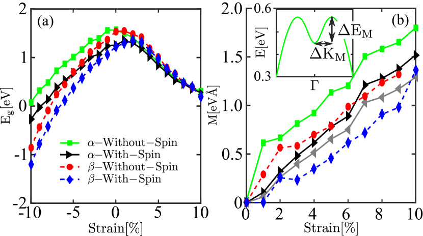
The variation range of strain is - from equilibrium condition. In the compressive strain regime, we find that although the horizontal distance of Ga-Te is shortened, the buckling heights in the vertical direction are increased for the GaTe monolayer. The charge redistribution is weaken duration the compressive strain and the band-gap is decreased. In this strain range, although CBM is in the M point, a strain-induced self-doping occurs due to the movement of bands at the point. In the tensile strain regime, though the horizontal distance of Ga-Te is increased and the buckling heights in the vertical direction is increased for the GaTe monolayer. The charge redistribution is strength duration the tensile strain and the band-gap decreases. Band-gap for two phases approximately is the same in tensile regime and differences between these two band-gaps increases by moving from tensile to compressive regime. phase relative to phase has a higher band-gap in compressive regime. Therefore, the effect of strain in phase is lower than phase.
SOC in phase is similar to phase, for example, in the strain, the differences between band-gap with and without SOC in and phases is and , respectively. Another result of Fig. 2 is due to the strain, GaTe in phase could be phase transition from semiconductor to semi-metal in strain whereas phase remains semiconductor in this strain.
The valence band maximum shifted to point by the compressive strain and dismiss Mexican-hat dispersion. At the other hand, the tensile strain regime shows the Mexican-hat-shaped dispersion Cao et al. (2015) in the band structure and increases the density of state in valance bands (Fig. 2). We obtained Mexican-hat coefficient with SOC for both phases in up and down components spin whereas in phase these two components are degenerated. Mexican-hat coefficient can be defined as: where and are energy and momentum differences between VBM and -point, respectively, see the inset of Fig. 2(b). In phase, Mexican-hat has higher value than the phase. SOI decreases Mexican-hat coefficient for two phases. For example, in strain, SOC decreases Mexican-hat coefficient which this decreasing ratio approximately hold for other percentage of strain in tensile regime. As can be seen from the Fig. 2, up-spin component of phase shows higher Mexican-hat relative to down component and their difference increases with increment of strain.

We study the band gap and Mexican-hat dispersion with applying uniaxial strain in two Armchair and Zigzag directions that is shown in the Fig. 3. Our finding indicates that the gap with- and without-SOC changes respect to the strain and shows the same behavior in both directions. Band gap decreases with increasing strain in compression regime. In the tensile strain regime, band gap decreases by increasing strain. For both directions and both structures ( and ), SOC declines band gap relative to without SOC.
The Mexican-hat coefficient increases with increasing strain in both Armchair and Zigzag strains. In the structure, Mexican-hat is higher than the structure. SOC declines Mexican-hat for both strain directions in two structures. For example, in structure, SOC approximately decreases Mexican-hat by 4 times, Whereas, SOC decreases this coefficient lower than 2 times for biaxial strain. Mexican-hat coefficient is calculated for two spins (up and down). For structure these two coefficients is the same because of spin degeneracy in this structure due to inversion symmetry. structure with no inversion symmetry, shows two Mexican-hats for both separated spins. By applying Armchair strain, VBM is located at direction and there isn’t any spin-splitting due to spin degeneracy in this direction. At the other hand, MVB is placed in direction and one can obtain two Mexican-hat coefficients for both spins.
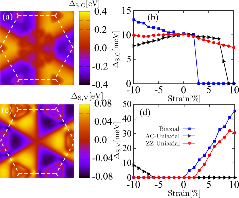
Fig. 4 shows the calculations of the spin-splitting of the uppermost valence band and the lowermost conduction band in monolayer GaTe for phase at biaxial, Armchair and Zigzag uniaxial strains. GaTe in phase doesn’t induce spin-splitting due to the inversion symmetry. Spin-splitting in conduction and valence bands at Brillouin zone is reported in the Fig 4 (a) and (c), respectively. In the conduction band, between M point to M’ point (area 1) spin-splitting is positive whereas between M’ to M point (area 2) is negative. This indicates the up-spin energy is higher than the down-spin energy at area 1, and vice versa at area 2. Spin-splitting, for the valence band, at area 1 is negative and at area 2 is positive. decreases by increasing biaxial strain. For strain higher than , CBM is located at point and there isn’t any spin-splitting. However, for lower than , CBM is placed at point. In compressive regime, as Ga-Te atom distances decreases, increasing of potential gradient causes to SOC increasing . VBM is located at point for compressive strain then vanished. Whereas, VBM is located at point for all strains in Armchair direction, therefore spin-splitting goes to zero. Due to VBM move to and take a distance from point. vector can be defined as distance between and . increases by tensile strain increasing and increases as increasing.
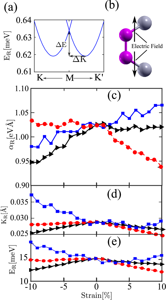
Rashba effect can play an important role in future spintronic. The Rashba effect happens due to the structural asymmetry causes an out-of-plane electric field whereas, GaTe with mirror symmetry shouldn’t show any Rashba effect but it constructed from two sub-layers that each sub-layer has an out-of-plane asymmetry. An electric field is originated from this asymmetry, see Fig. 5. For a two-dimensional electron gas the Rashba Hamiltonian is defined by:
| (1) |
Where is the Rashba parameter, is the Pauli matrices, is the in-plane momentum of the electrons, and is the out-of-plane unit vector Bychkov and Rashba (1984). can be defined as where is Rashba energy and is momentum offset, see Fig.5(a). However, and stabilize spin precession and make a phase offset for different spin channels in the spin-field effect transistor device Absor et al. (2018b). Rashba-split dispersion for phase is reported in Fig. 5. This figure shows increases with increasing the strain in biaxial strain that is in agreement with Ref.[Ma et al., 2014]. By increasing strain, distance between Ga sublayers and Te sublayers decreases which causes to enhance out-of-plane electric field. Rashba parameter increases in the Armchair strain in compressive regime and reaches to a constant amount in tensile regime. In compressive regime Armchair strain declines these two sub-layers. Whereas, Zigzag strain is in the opposite of Armchair strain.
One can observe the results of the parameters , , and in Table. 1, and compare with some materials for previously reported references. We find the amount of is 1.03 for equilibrium condition and 1.07 for strain. However, is the largest calculated value under biaxial strain, but in this strain, CBM is located at point. For the comparison with the other papers, Rashba parameters is obtained 1.03 for no strain which in this strain CBM is placed at M point. Our is larger than GaSe/MoSe2 heterostructure Zhang and Schwingenschlögl (2018), Janus Transition Metal Dichalcogenides Li et al. (2017); Yao et al. (2017), comparable with Br-doped PtSe2 Absor et al. (2018b) and lower than LaOBiS2 Liu et al. (2013), BiSb Singh and Romero (2017),BiTeI Ma et al. (2014), I-doped PtSe2 Absor et al. (2018b). indicates potential barrier between two spin. in the strained GaTe is lower than Bi/Ag(111) interface, LaOBiS2 and BiTeI. However, monolayer WSeTe and GaSe/MoS2 heterostructure show higher but strained GaTe shows higher and comparable relative some reported previously. For instance, GaTe shows higher amount relative to I- and B-doped PtSe2, WSSe and MoSSe. These results approves GaTe can be a good candidate for future spintronic.
| 2D-ML | |||
|---|---|---|---|
| GaTe ( ) | 14.9 | 0.0288 | 1.03 |
| GaTe () | 15.5 | 0.029 | 1.07 |
| LaOBiS2 Liu et al. (2013) | 38 | 0.025 | 3.04 |
| BiSb Singh and Romero (2017) | 13 | 0.0113 | 2.3 |
| BiTeI Ma et al. (2014) | 39.8 | 0.043 | 1.86 |
| I-doped PtSe2 Absor et al. (2018b) | 12.5 | 0.015 | 1.7 |
| Br-doped PtSe2 Absor et al. (2018b) | 4.91 | 1.07 | |
| WSeTe Yao et al. (2017) | 52 | 0.17 | 0.92 |
| WSSe Li et al. (2017) | 3.6 | 0.010 | 0.72 |
| MoSSe Li et al. (2017) | 1.4 | 0.005 | 0.53 |
| GaSe/MoSe2 heterostructure Zhang and Schwingenschlögl (2018) | 31 | 0.13 | 0.49 |
| Surface | |||
| Bi/Ag (111) Ast et al. (2007) | 200 | 0.13 | 3.05 |
| Bi (111) Koroteev et al. (2004) | 14 | 0.05 | 0.55 |
| Interface | |||
| InGaAs/InAlAs Nitta et al. (1997) | 0.028 | 0.07 |
In conclusion, using first-principles density functional calculations, we have investigated systematically the spintronic properties in two-dimensional GaTe. Two structures, with mirror symmetry and with inversion symmetry is considered. This study suggests band gap can be tuned under biaxial, AC-uniaxial and ZZ-uniaxial strains with and without spin-orbit coupling. SOI causes to band gap shows lower amount. In the tensile and compressive strain, the band gaps of GaTe decreased by increasing strain amount. Although, the band gap more decreases by consideration of SOC. The AC-strain and ZZ-strain apply a similar effect on the band gap of GaTe. We observe Mexican-hat only in the case of tensile strain and Mexican-hat increases with strain increasing. SOI implies to smoother Mexican-hat dispersion. In biaxial strain, The spin-splitting declines with increment of strain. GaTe indicates Rashba effect that Rashba parameters can be tuned a little by strain.
References
- Novoselov et al. (2004) K. S. Novoselov, A. K. Geim, S. V. Morozov, D. Jiang, Y. Zhang, S. V. Dubonos, I. V. Grigorieva, and A. A. Firsov, Science 306, 666 (2004).
- Wang et al. (2014) H. Wang, X. Wang, F. Xia, L. Wang, H. Jiang, Q. Xia, M. L. Chin, M. Dubey, and S.-j. Han, Nano Lett. 14, 6424 (2014).
- Huang et al. (2016) S. Huang, Y. Tatsumi, X. Ling, H. Guo, Z. Wang, G. Watson, A. A. Puretzky, D. B. Geohegan, J. Kong, J. Li, et al., ACS Nano 10, 8964 (2016).
- Guo et al. (2015) R. Guo, X. Wang, Y. Kuang, and B. Huang, Phys. Rev. B 92, 115202 (2015).
- Fei and Yang (2014) R. Fei and L. Yang, Nano Lett. 14, 2884 (2014).
- Li et al. (2012) Y. Li, F. Li, and Z. Chen, J. Am. Chem. Soc. 134, 11269 (2012).
- Elias et al. (2009) D. C. Elias, R. R. Nair, T. Mohiuddin, S. Morozov, P. Blake, M. Halsall, A. Ferrari, D. Boukhvalov, M. Katsnelson, A. Geim, et al., Science 323, 610 (2009).
- Ma et al. (2012) Y. Ma, Y. Dai, M. Guo, C. Niu, Z. Zhang, and B. Huang, Phys. Chem. Chem. Phys. 14, 3651 (2012).
- Zhou et al. (2009) J. Zhou, M. M. Wu, X. Zhou, and Q. Sun, Appl. Phys. Lett. 95, 103108 (2009).
- Koppens et al. (2014) F. Koppens, T. Mueller, P. Avouris, A. Ferrari, M. Vitiello, and M. Polini, Nat. Nanotechnol. 9, 780 (2014).
- Hu et al. (2014) P. Hu, J. Zhang, M. Yoon, X.-F. Qiao, X. Zhang, W. Feng, P. Tan, W. Zheng, J. Liu, X. Wang, et al., Nano Research 7, 694 (2014).
- Rao et al. (2015) C. Rao, K. Gopalakrishnan, and U. Maitra, ACS Appl. Mater. Interfaces 7, 7809 (2015).
- Şahin and Ciraci (2011) H. Şahin and S. Ciraci, Phys. Rev. B 84, 035452 (2011).
- Sheng et al. (2012) Z.-H. Sheng, H.-L. Gao, W.-J. Bao, F.-B. Wang, and X.-H. Xia, J. Mat. Chem. 22, 390 (2012).
- Cocco et al. (2010) G. Cocco, E. Cadelano, and L. Colombo, Phys. Rev. B 81, 241412 (2010).
- Gui et al. (2008) G. Gui, J. Li, and J. Zhong, Phys. Rev. B 78, 075435 (2008).
- Rybkovskiy et al. (2014) D. V. Rybkovskiy, A. V. Osadchy, and E. D. Obraztsova, Phys. Rev. B 90, 235302 (2014).
- Wickramaratne et al. (2014) D. Wickramaratne, F. Zahid, and R. K. Lake, J. Chem. Phys 140, 124710 (2014).
- Cao et al. (2015) T. Cao, Z. Li, and S. G. Louie, Phys. Rev. Lett. 114, 236602 (2015).
- Zólyomi et al. (2013) V. Zólyomi, N. D. Drummond, and V. I. Fal’ko, Phys. Rev. B 87 (2013).
- Wu et al. (2014) S. Wu, X. Dai, H. Yu, H. Fan, J. Hu, and W. Yao, arXiv preprint arXiv:1409.4733 (2014).
- Magorrian et al. (2016) S. Magorrian, V. Zólyomi, and V. Fal’ko, Phys. Rev. B 94, 245431 (2016).
- Lifshitz et al. (1960) I. Lifshitz et al., Sov. Phys. JETP 11, 1130 (1960).
- Wickramaratne et al. (2015) D. Wickramaratne, F. Zahid, and R. K. Lake, J. Appl. Phys. 118, 075101 (2015).
- Do et al. (2015) D. T. Do, S. D. Mahanti, and C. W. Lai, Sci. Rep. 5, 17044 (2015).
- Bychkov and Rashba (1984) Y. A. Bychkov and E. I. Rashba, JETP lett 39, 78 (1984).
- Datta and Das (1990) S. Datta and B. Das, Appl. Phys. Lett. 56, 665 (1990).
- Absor et al. (2018a) M. A. U. Absor, H. Kotaka, F. Ishii, and M. Saito, Jpn. J. Appl. Phys. 57, 04FP01 (2018a).
- Zhang and Schwingenschlögl (2018) Q. Zhang and U. Schwingenschlögl, Phys. Rev. B 97, 155415 (2018).
- Premasiri et al. (2018) K. Premasiri, S. Kumar, S. Sucharitakul, R. K. Ulaganathan, R. Sankar, F.-C. Chou, Y.-T. Chen, and X. P. Gao, Nano Lett. (2018).
- Nitta et al. (1997) J. Nitta, T. Akazaki, H. Takayanagi, and T. Enoki, Phys. Rev. Lett. 78, 1335 (1997).
- LaShell (1996) S. LaShell, Phys. Rev. Lett. 77, 3419 (1996).
- Žutić (2004) I. Žutić, Rev. Mod. Phys. 76, 323 (2004).
- Kimura et al. (2010) A. Kimura, E. Krasovskii, R. Nishimura, K. Miyamoto, T. Kadono, K. Kanomaru, E. Chulkov, G. Bihlmayer, K. Shimada, H. Namatame, et al., Phys. Rev. Lett. 105, 076804 (2010).
- Konschuh et al. (2010) S. Konschuh, M. Gmitra, and J. Fabian, Phys. Rev. B 82, 245412 (2010).
- Cheng et al. (2013) Y. Cheng, Z. Zhu, M. Tahir, and U. Schwingenschlögl, Europhys. Lett. 102, 57001 (2013).
- Liu et al. (2013) Q. Liu, Y. Guo, and A. J. Freeman, Nano Lett. 13, 5264 (2013).
- Min et al. (2006) H. Min, J. Hill, N. A. Sinitsyn, B. Sahu, L. Kleinman, and A. H. MacDonald, Phys. Rev. B 74, 165310 (2006).
- Ishizaka (2011) K. Ishizaka, Nat. Mater. 10, 521 (2011).
- Ast et al. (2007) C. R. Ast, J. Henk, A. Ernst, L. Moreschini, M. C. Falub, D. Pacilé, P. Bruno, K. Kern, and M. Grioni, Phys. Rev. Lett. 98, 186807 (2007).
- Koroteev et al. (2004) Y. M. Koroteev, G. Bihlmayer, J. Gayone, E. Chulkov, S. Blügel, P. M. Echenique, and P. Hofmann, Phys. Rev. Lett. 93, 046403 (2004).
- Lee et al. (2015) K. Lee, W. S. Yun, and J. Lee, Phys. Rev. B 91, 125420 (2015).
- Žutić et al. (2004) I. Žutić, J. Fabian, and S. D. Sarma, Rev. Mod. Phys. 76, 323 (2004).
- Zhang et al. (2015) S. Zhang, Z. Yan, Y. Li, Z. Chen, and H. Zeng, Angewandte Chemie 127, 3155 (2015).
- Giannozzi et al. (2009) P. Giannozzi, S. Baroni, N. Bonini, M. Calandra, R. Car, C. Cavazzoni, D. Ceresoli, G. L. Chiarotti, M. Cococcioni, I. Dabo, et al., J. Phys.:Condensed Matter 21, 395502 (2009).
- Giannozzi et al. (2017) P. Giannozzi, O. Andreussi, T. Brumme, O. Bunau, M. B. Nardelli, M. Calandra, R. Car, C. Cavazzoni, D. Ceresoli, M. Cococcioni, et al., J. Phys.:Condensed Matter 29, 465901 (2017).
- Blöchl (1994) P. E. Blöchl, Phys. Rev. B 50, 17953 (1994).
- Kresse and Joubert (1999) G. Kresse and D. Joubert, Phys. Rev. B 59, 1758 (1999).
- Perdew et al. (2008) J. P. Perdew, A. Ruzsinszky, G. I. Csonka, O. A. Vydrov, G. E. Scuseria, L. A. Constantin, X. Zhou, and K. Burke, Phys. Rev. Lett. 100, 136406 (2008).
- Ge et al. (2017) X.-J. Ge, D. Qin, K.-L. Yao, and J.-T. Lü, J. Phys. D: Appl. Phys. 50, 405301 (2017).
- Cai et al. (2016a) H. Cai, J. Kang, H. Sahin, B. Chen, A. Suslu, K. Wu, F. Peeters, X. Meng, and S. Tongay, Nanotechnology 27, 065203 (2016a).
- Cai et al. (2016b) H. Cai, E. Soignard, C. Ataca, B. Chen, C. Ko, T. Aoki, A. Pant, X. Meng, S. Yang, J. Grossman, et al., Adv. Mater. 28, 7375 (2016b).
- Huang et al. (2015) L. Huang, Z. Chen, and J. Li, RSC Advances 5, 5788 (2015).
- Zhuang and Hennig (2013) H. L. Zhuang and R. G. Hennig, Chem. Mater. 25, 3232 (2013).
- Absor et al. (2018b) M. A. U. Absor, I. Santoso, K. Abraha, H. Kotaka, F. Ishii, M. Saito, et al., Phys. Rev. B 97, 205138 (2018b).
- Ma et al. (2014) Y. Ma, Y. Dai, W. Wei, X. Li, and B. Huang, Phys. Chem. Chem. Phys. 16, 17603 (2014).
- Li et al. (2017) F. Li, W. Wei, P. Zhao, B. Huang, and Y. Dai, J. Phys. Chem. Lett 8, 5959 (2017).
- Yao et al. (2017) Q.-F. Yao, J. Cai, W.-Y. Tong, S.-J. Gong, J.-Q. Wang, X. Wan, C.-G. Duan, and J. Chu, Phys. Rev. B 95, 165401 (2017).
- Singh and Romero (2017) S. Singh and A. H. Romero, Phys. Rev. B 95, 165444 (2017).