Nonlinear plasmonic switching in graphene stub nanoresonator loaded with core-shell quantum dot
Abstract
We study theoretically a problem of nonlinear interaction between two surface plasmon-polariton (SPP) modes propagating along the graphene waveguide integrated with a stub nanoresonator loaded with a core-shell quantum dot (QD). The conditions of strong coupling and very narrowband resonance for Ladder-type SPP-QD interaction in nanoresonator leading to -phase shift of signal SPP mode are established and discussed. Using the full-wave electromagnetic simulation we demonstrate that turning on the pump SPP leads to a transition from destructive to constructive interference in the stub nanoresonator and subsequent effect of switching from locking to transmitting the signal SPP through the waveguide. On the base of the obtained results we develop the model of all-plasmonic graphene transistor with optimized characteristics including the size about nm and the clock frequency about GHz functioning at the near-infrared wavelength range.
pacs:
I Introduction
The achievements of modern 2D material science Aliofkhazraei et al. (2016); Britnell et al. (2012); Tonndorf et al. (2015); Srivastava et al. (2015), graphene nanotechnologies Freitag et al. (2016) and quantum nanophotonics Bozhevolnyi et al. (2017) give hope to the experimental implementation of a new information processing gate with record values of transistor size and clock frequency in the soon time. The major premise of this implementation is the new methods of single photon states control Hausmann et al. (2012) and manipulation of single plasmons Thakkar et al. (2015) and surface plasmon-polaritons (SPPs) Vasa and Lienau (2018); Stebunov et al. (2018) under strong-coupling condition González-Tudela et al. (2013). Moreover, the control of plasmonic resonance for nanostructures placed near a graphene layer Chen et al. (2013) in condition of strong coupling González-Tudela et al. (2013) may provide the realization of complete quantum computing protocols Kovlakov et al. (2017) at a subwavelength scale. At the same time, the expected achieving of high-temperature superconductivity in graphene and doped graphene Zhou et al. (2015); García de Abajo (2014) should solve the key problem of huge losses, which restricts the implementation of plasmonic nanostructures Wu et al. (2017) in computer technologies. In this context, plasmonic information processing circuits using graphene-localized SPPs as information carriers and quantum dots (QDs) Fedorov et al. (2007) as information processing centers can be considered as good candidates for replacing of existing electronic circuits.
However, even under ideal conditions of strong coupling and ultra-low losses, the problem of very broadband plasmon-exciton resonance remains relevant for semiconductor quantum dots. The solution of this problem may consist in the using narrowband resonances Evlyukhin and Bozhevolnyi (2015) and positive feedback of nanoresonator Cao et al. (2018). The stub resonator Lin and Huang (2008) used for broadband signal filtering can be chosen as a technological platform for this solution. Such resonators are usually made from a combination of metal and dielectric. However, application of graphene Liu et al. (2016) and nanostructured graphene resonators Kong et al. (2015) loaded with 0-D chromophores can help to implement the well-known effects of matter-field interactions such as nonlinear wave mixing Cox and García de Abajo (2015), Fano resonance Iorsh et al. (2013); Gelin and Bondarev (2016), slow light Kim et al. (2018) and others Britnell et al. (2013); Stebunov et al. (2015) for creating of plasmonic graphene circuits at infrared radiation (IR) range. Additional mode selections and enhance in the efficiency of plasmon-exciton interactions in such systems can be obtained by using chiral QDs Puri and Ferry (2017).
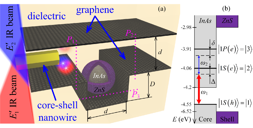
In presented work, we carry out a fundamental research of interaction between graphene-like materials and semiconductor quantum dots. Following to Ref. 30, we propose to integrate a stub nanoresonator with the graphene waveguide, and to load a core-shell quantum dot (QD) into stub for the realization of plasmon-exciton resonance, see Fig. 1. In this configuration, the combination of the nanoresonator with the waveguide can lead to a significant narrowing of plasmon-exciton resonance spectral line and precise tuning of the system to the working wavelength. Moreover, we choose an additional strong pump SPP mode for the realization of controllable switching between two stable states of the signal SPP mode using three-level Ladder-type scheme of SPP-QD interaction by analogy with optics Lukin et al. (1997); Vadeiko et al. (2005). The key idea of our work is to use a strong nonlinear interaction between the signal and pump SPPs in a nanoresonator loaded with QD to control the phase shift and transmittance of signal SPP through the stub due to the changing of pump SPP intensity and its detuning. This is necessary to achieve radians phase shift of signal SPP, under which a change in the SPP pattern from destructive to constructive interference in nanoresonator occurs. The use of a core-shell QD is aimed on decreasing the nonradiative relaxation rate Reiss et al. (2009) and solving the blinking problem Osad’ko et al. (2015). Thus, the main goal of this paper is to investigate and optimize the material parameters and geometric characteristics of nanoresonator loaded with QD in order to get the all-plasmonic gates at the nanoscale for IR range. To accomplish this goal, we will adhere to the semiclassical approximation for the description of nonlinear plasmon-exciton interactions, as well as the strong coupling condition to obtain the steady-state solutions for signal SPP in both basic states of device. The necessary technical equipment and the applicability of various process-technologies for the practical creation of the described devices are discussed.
In the technical framework, the presented stub nanoresonator loaded with QD can be used for practical implementation of all-plasmonic transistors. The use of graphene as a basis for such devices, potentially, allows us to work beyond adiabatically approximation and manipulate with ultrafast electromagnetic fields Kelardeh et al. (2015a). Such devices can be integrated into plasmonic circuits Lemke et al. (2014) supported terahertz clock frequency and the nanometer gate scale.
II Results and discussion
Let us to consider the system of graphene waveguide based on the pair of graphene sheets and graphene stub nanoresonator loaded with a core-shell quantum dot, see. Fig. 1a. The IR fields and convert into SPP modes and , respectively, propagating in waveguide at the same frequencies than IR fields. We assume that a signal SPP mode with frequency inputs into the system through Port 1. From the experimental point of view, SPPs could be generated in graphene waveguide using special tips of a near-field optical microscope simulating of both either electric dipole (ED) or magnetic dipole (MD) sources Picardi et al. (2017); le Feber et al. (2015). However, this approach is good only for a laboratory experiment, since the tip sizes are still large comparing with the scales of the designed plasmonic gates. Therefore, it is necessary to integrate core-shell nanoparticles Arnold et al. (2016) or nanowires Ho et al. (2015) into the circuit to use them as sources of near field, see Fig. 1a. In our simulation we use MD source.
During the propagation SPP mode interacts with QD in Port 3 and leaves the system via Port 2 corresponding to the output of the circuit. The dispersion relation for SPPs propagation constants can be written in the form Wang et al. (2012a)
| (1) |
where is the total conductivity of graphene, , is the speed of light in vacuum, , is the vacuum permittivity, is the permittivity of the dielectric material between the graphene sheets with a distance between them. The pump SPP mode can also propagate in the graphene waveguide in Fig. 1a. Assuming that both SPPs interact with QD loaded in nanoresonator we will investigate the features of SPP mode patterns in waveguide for their simultaneous and separate propagation.
The surface conductivity of graphene in the near-infrared range is given by the Kubo formula Falkovsky and Pershoguba (2007) which consists of the intraband conductivity and interband conductivity and have the following forms:
| (2a) | |||||
| (2b) | |||||
where is the Boltzmann constant, is the temperature, is the chemical potential, is the carrier-scattering rate, and is the electron charge, is the Planck constant. For simulation, we set the effective thickness of graphene as , (this value is typical for doped graphene), , , wavelength of signal SPP mode , which configures the device to use it in infrared data transmission and processing systems.
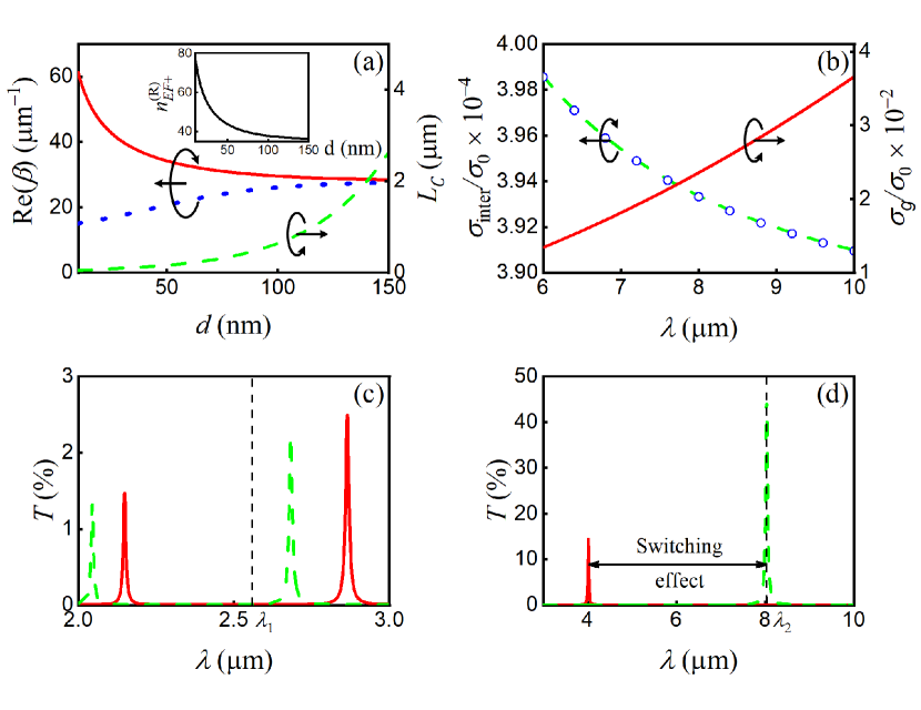
The propagation constants of the symmetric and anti-symmetric modes as a function of the distance between graphene sheets are presented in Fig. 2a. The space between sheets is filled with a dielectric . We will discuss the symmetric mode only because it leads to the highest density of electromagnetic field in the space between sheets. It is necessary to increase the efficiency of matter-field interaction with chromophore loaded in the stub nanoresonator Wang et al. (2012a). We choose , which determines a regime of strong coupling between sheets satisfying to condition Wang et al. (2012b), where . Based on the solution of equation (1), the estimations can be given for the other main characteristics of SPP propagation in the graphene waveguide, including SPP wavelength , coupling length and propagation length . Here is the coupling constant of SPPs and is the effective refractive index. In our case, we have , , , for signal SPP. These estimations allow to achieve about stub-nanoresonators at the distance equals to propagation length. The obtained values of the main parameters are in good agreement with the result of full-wave electromagnetic simulation based on FDTD (Finite Difference Time Domain) method Sullivan (2000). We realized FDTD method by ourselves (see Fig. 3) and tested it using other simulations for graphene Wang et al. (2012a); Sarker et al. (2017); Hossain and Rana (2015).
We start with tuning the parameters of the passive stub so that in the absence of SPP mode it does not transmit SPP mode to the right side of the stub (Port 2). We optimized the height of stub resonator to achieve a transmittance minimum Lin and Huang (2008) at the signal wavelength for a given stub width . Since the phase shift in such a resonator is determined by the expression
| (3) |
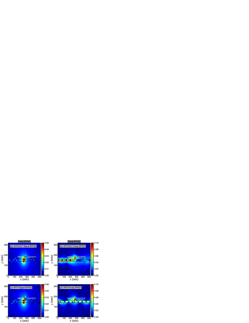
then from condition we obtain for . Here is the additional phase shift results from the material properties inside the stub resonator. We can neglect it owing to the absence of pump SPP, because signal SPP doesn’t interact with QD in the stub separately from the pump SPP. Then, the signal SPP at the wavelength has a destructive interference and locked by the stub, see Fig. 3b.
The dependencies of the transmittance coefficient
are shown in Fig. 2c,d, where parameters , , corresponds to the reflection, transmission and splitting coefficients in the th cross-section (th Ports) of the stub from Fig. 1a. These coefficients can be physically explained from the scattering matrix theory Haus (1984) and expressed in terms of characteristic impedances of media, surface modification and geometry of the system. In addition, they can be directly extracted using FDTD method Kocabas et al. (2008). By varying the material parameters and profile of the substrate for the graphene sheet Kong et al. (2015); Gu et al. (2015), it is possible to achieve very narrow transmittance peaks at the selected wavelength, see Fig. 2c,d. However, using our tunings the transmittance for signal SPP is almost zero at and the SPP does not propagate to the right side of the stub (see Fig. 3b).
We will now consider the possibility to control the SPP propagation due to plasmonic resonance with nanostructures Chen et al. (2013). Therefore, we proceed to consider the matter-wave interaction between QD and SPP in the graphene stub nanoresonator loaded with core-shell QD. Using the semi-classical approximation we describe the Ladder-type SPP-QD interaction, as well as within the density matrix formalism we describe the three-level scheme of electron/hole sublevels in QD, see Fig. 1b. The Hamiltonian of the system QD+SPPs has the following form:
| (4a) | |||||
| (4b) | |||||
| (4c) | |||||
where is the Hamiltonian of unexcited QD and is the Hamiltonian of SPP-QD interaction, and are the Rabi frequencies of pump and signal SPPs, respectively, and are the slowly varying amplitudes of Rabi frequencies, and are the frequencies of pump and signal SPPs, respectively, and are the frequencies of transitions in QD. Here the pump SPP mode is tuned to the interband transition while the signal SPP mode is tuned to the intraband transition . We note that in the absence of pump SPP levels and are empty and signal SPP doesn’t interact with QD, therefore .
From a mathematical point of view, the novelty of our approach is the exploitation of nonlinear regime of SPP-QD interaction corresponds to the two-quantum transitions between levels and in the case , where is the frequency detuning (see Fig. 1b) and is the rate of decay between levels and Gubin et al. (2018); Shesterikov et al. (2018). Note, that the relaxation rates of QD have a dramatic increase only at the certain distance to the conductive mirror Larkin et al. (2004), but there exist optimized distances with maximum efficiency of energy conversion from QD into SPP Gubin et al. (2019). Then, under the condition , the SPP mode provides the effective non-linear phase modulation of signal SPP. The key idea is to tune the pump SPP parameters so that the phase shift of signal SPP will be radians. This is the basis for realization of the switching effect and creation of all-plasmonic transistor.
Based on the known material parameters of graphene and semiconductors we use the core-shell InAs/ZnS QD Bouarissa and Aourag (1999); Cao and Banin (2000) to achieve our goal, see. Fig. 1a. The resonant frequencies of the corresponding transitions can be obtained in the form
| (5a) | |||||
| (5b) | |||||
where is the band gap of InAs, , are the effective masses of electron and hole, respectively; and are the roots of the Bessel function. The dipole moment of the intraband transition can approximately be estimated by the relation Madelung et al. (2002), where and is the radius of the QD core with dielectric permittivity ; the dielectric permittivity of the shell is . The square of dipole moment of the interband transition can be found from Ref. 59:
where is the spin-orbit splitting for InAs. All parameters of QD are determined by using our numerical simulator pla and the initial data from the literature Bouarissa and Aourag (1999); Cao and Banin (2000).
We determine the QD size from (5b) based on the condition and obtain . According to this QD core size and additional condition for pump SPP, we have determined resonance wavelength , as well as the values of the dipole moments and for interband and intraband transitions, respectively. We note that pump field is also localized on graphene waveguide (see Fig. 3a,c), but pump SPP propagates in the weak coupling regime (). At the same time, the week coupling regime is compensated by a high intensity of the pump field at the input. The transmittance for pump SPP at the wavelength is not so high for both cases with and without signal SPP, see Figs. 2c and 3a,c.
The implementation of two SPPs and in the circuit leads to the appearance of polarization for transition . We used the Liouville master equation with Hamiltonian (4) and assumption of unchanged polarization (i.e. ) to derive the nonlinear equation for dynamics of density matrix element :
| (6) |
where corresponds to the induced single-quantum transitions in the system; corresponds to the nonlinear cross-interaction between SPP modes, and corresponds to the nonlinear modulation of signal SPP induced by interaction with the pump field; corresponds to the linear effects associated with the dispersion and spontaneous decay of the excited states; is the frequency detuning of signal SPP, see Fig. 1b. Now, we represent the Rabi frequencies in the form and for pump and signal SPP modes, respectively, with average numbers of plasmon-polaritons and . The parameters and determine the population imbalance and the rate of decay between levels and , respectively.
Applying the stationary conditions (i.e. ) to our system allows to obtain the steady-state solutions for the polarizations (see Fig. 4d) in the following form Gauthier (2003):
| (7a) | |||||
| (7b) | |||||
where , , , is the stationary value of population imbalance between levels and . The coupling SPP-QD constants have the form
where the effective volume can be taken as , and is specified by the SPP mode distribution in the stub, and it can be obtained by the FDTD method Lin and Huang (2008). The values of the coupling constants will be and for the selected parameters provided that the location of QD is in the geometrical center of the stub and taking into account the calculated intensities of signal and pump SPPs inside the stub, see. Fig. 3.
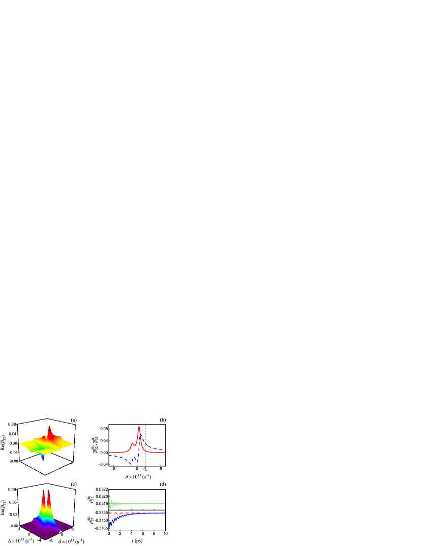
In order for the transistor to be opened, the additional phase shift should be . In this case, the first order maximum of SPP mode will be precisely tuned to the wavelength of , see Fig. 2d. In order to determine the required parameters of pump SPP mode , we represent the expression for the phase shift in the form , where is the complex nonlinear refractive index of QD, see Fig. 4a–c. The nonlinear refractive index , where , is the carrier concentration of InAs Madelung et al. (2002), , , . Thus, we get the possibility to control the pattern of signal SPP spatial distribution inside and at the output of stub Evlyukhin et al. (2009) (Port 3 in Fig. 1a) via parameters of the pump SPP mode.
As a signal mode, we choose a weak SPP with amplitude , the field strength is represented by formula (). The required phase shift is formed when the amplitude of the pump SPP mode is . In this case, the destructive interference will change to constructive and the transistor will be opened for signal SPP propagating to the right side of the stub (compare regimes b and d in Fig. 3). We note that the required regime can be achieved only under condition , when nonlinear interaction between SPPs and QD occurs most strongly. In the linear regime for cascade scheme with the polarization does not achieve the necessary value against the background of large losses, see Fig. 4b. In addition, we choose such combination of frequency detunings that the absorption of the signal SPP transmitted from Port 1 to Port 3 is kept low, see Fig. 4b,c. It takes place for the optimized values and and fixed values , , that corresponds to strong SPP-QD coupling regime in nanoresonator loaded with QD. Hence, we obtain and , (with stationary values of populations , , ).
The representation (6) for the polarization change rate allows us to understand the contribution of each linear (and nonlinear Dzedolik (2014); Dzedolik and Pereskokov (2017)) effects to the process of switching and achieving the stationary regime of SPP-QD interaction in the stub. In particular, the initial deviations for polarizations from the stationary values given by were used for simulation in Fig. 4d and led to the values of considered coefficients , , , . The stabilization process takes place such that the formation of a strong phase shift resulting from , and is compensated by nonlinear cross-interaction due to with opposite sign. On the other hand, the growth of linear losses resulting from is compensated by nonlinear induced amplification due to . As a result, the system finds its own balance between dispersion, absorption and nonlinear processes and tends to a stationary level of parameters, which is a necessary condition for the stable functioning of the plasmonic device.
Now, let us to pay attention to the key working parameters of the designed device. Firstly, it is a size of transistor, which in our case is about . Secondly, a clock frequency that is about and can be obtained from the characteristic stabilization time of the system approximately , see Fig. 4d. And thirdly, a length of SPP propagation that is in our case allowing to place about 150 elements within the circuit.
The special attention should be paid to the production of the all-plasmonic transistor discussed here. The process of creating a device requires the combination of several experimental techniques at once. At the first stage, PECVD (plasma enhanced chemical vapor deposition) method should be used to deposit a high-quality graphene monolayer Kim et al. (2014) on a silica substrate with a patterned stub.
Obviously, the stub corners cannot be right angles, as this will lead to the excessive stresses in graphene. The radius of curvature for the stub corners should be determined experimentally, but it must be more than according to the sampling interval in our FDTD method. Note that in such conditions we observe a high density of near field in the corners of resonator (see Fig. 3a,c), but this does not dramatically change the SPP propagation. At the second stage, the quantum dot need to be loaded into the stub using the nanomanipulation technique with atomic force microscope Ratchford et al. (2011). The next step is to coat the quantum dot and graphene sheet with dielectric by means of ALD (atomic layer deposition) method Jeon et al. (2016); Ahn et al. (2017). Finally, it is necessary to reapply PECVD method for deposition of second graphene layer on dielectric and ALD method for the final coating of device with a dielectric. We note that the field sources inside device can be implemented by core-shell nanowires Ho et al. (2015) integrated inside plasmonic circuit.
III Conclusion
In this paper we have considered the model of graphene stub nanoresonator loaded with a core-shell quantum dot to solve the problem of all-plasmonic control of SPP modes at the nanoscale. Based on the main parameters of graphene and InAs/ZnS semiconductors, we have investigated the physical properties, and their connections with geometric characteristics, of the stub nanoresonator and QD in order to realize switching between two stable states of a signal SPP mode using a pumping SPP. The strong coupling regime in the condition of Ladder-type nonlinear plasmon-exciton interaction scheme for QD loaded in the stub has been considered. As a result we have proposed the model of all-plasmonic transistor with working wavelength, characteristic size and clock frequency. The proposed transistor can be used for development of a new perspective in processors architecture. In contrast to classical electronic or all-optical gates our system can provide the switching effect for SPP modes in near-infrared range at the nanoscale, accompanied by very narrow resonance lines.
For practical realization of a new transistor, the strict account for a charge carrier mobility Kelardeh et al. (2015a) and memory effect Choi et al. (2018) in graphene are necessary. The solution of this problem requires the development of a new paradigm of material science directed on achievement of high-temperature superconductivity of graphene García de Abajo (2014) and graphene-like materials Kelardeh et al. (2015b). Moreover it addresses to 2D stack-structures based on a combination of monolayers with different physical properties and QDs Palacios-Berraquero et al. (2016); Praveena et al. (2017); Britnell et al. (2013); Kim et al. (2018). The greatest interest here is associated with the realization of gates on the basis of graphene nanoresonators with QDs supporting magnetic dipole Freitag et al. (2016); Khokhlov et al. (2017), quadrupole Arnold et al. (2015), or anapole-like responses Zenin et al. (2017). Next development of the semiclassical Shesterikov et al. (2017) and full-quantum electrodynamics theory Bondarev (2015); Gubin et al. (2018) of near-field interactions in such systems should be continued as well.
Acknowledgements.
A.V. Prokhorov thanks Prof. M.I. Stockman and Prof. A.B. Evlyukhin for helpful discussions. This work was supported by Foundation for Assistance to Small Innovative Enterprises (FASIE), Grant No. 2226GS1/37022 (START-1) and by Russian Foundation for Basic Research (project no. 17-42-330001_r_a).References
- Aliofkhazraei et al. (2016) M. Aliofkhazraei, N. Ali, W. I. Milne, C. S. Ozkan, S. Mitura, and J. L. Gervasoni, Graphene science handbook. Electrical and Optical Properties (CRC Press, Taylor & Francis Group, LLC, Boca Raton, London, New York, 2016).
- Britnell et al. (2012) L. Britnell, R. V. Gorbachev, R. Jalil, B. D. Belle, F. Schedin, M. I. Katsnelson, L. Eaves, S. V. Morozov, A. S. Mayorov, N. M. R. Peres, A. H. Castro Neto, J. Leist, A. K. Geim, L. A. Ponomarenko, and K. S. Novoselov, Nano Lett. 12, 1707 (2012).
- Tonndorf et al. (2015) P. Tonndorf, R. Schmidt, R. Schneider, J. Kern, M. Buscema, G. A. Steele, A. Castellanos-Gomez, H. S. J. van der Zant, S. M. de Vasconcellos, and R. Bratschitsch, Optica 2, 347 (2015).
- Srivastava et al. (2015) A. Srivastava, M. Sidler, A. V. Allain, D. S. Lembke, A. Kis, and A. Imamoğlu, Nat. Nanotechnol. 10, 491 (2015).
- Freitag et al. (2016) N. M. Freitag, L. A. Chizhova, P. Nemes-Incze, C. R. Woods, R. V. Gorbachev, Y. Cao, A. K. Geim, K. S. Novoselov, J. Burgdorfer, F. Libisch, and M. Morgenstern, Nano Lett. 16, 5798 (2016).
- Bozhevolnyi et al. (2017) S. I. Bozhevolnyi, L. Martin-Moreno, and F. Garcia-Vidal, Quantum Plasmonics (Springer Series in Solid-State Sciences, 2017).
- Hausmann et al. (2012) B. J. M. Hausmann, B. Shields, Q. Quan, P. Maletinsky, M. McCutcheon, J. T. Choy, T. M. Babinec, A. Kubanek, A. Yacoby, M. D. Lukin, and M. Lonc̆ar, Nano Lett. 12, 1578 (2012).
- Thakkar et al. (2015) N. Thakkar, C. Cherqui, and D. J. Masiello, ACS Photonics 2, 157 (2015).
- Vasa and Lienau (2018) P. Vasa and C. Lienau, ACS Photonics 5, 2 (2018).
- Stebunov et al. (2018) Y. V. Stebunov, A. V. Arsenin, and V. S. Volkov, “Chapter 12 chemically derived graphene for surface plasmon resonance biosensing,” in Chemically Derived Graphene: Functionalization, Properties and Applications, edited by J. Zhang (The Royal Society of Chemistry, 2018) pp. 328–353.
- González-Tudela et al. (2013) A. González-Tudela, P. A. Huidobro, L. Martín-Moreno, C. Tejedor, and F. J. García-Vidal, Phys. Rev. Lett. 110, 126801 (2013).
- Chen et al. (2013) H.-A. Chen, C.-L. Hsin, Y.-T. Huang, M. L. Tang, S. Dhuey, S. Cabrini, W.-W. Wu, and S. R. Leone, J. Phys. Chem. C 117, 22211 (2013).
- Kovlakov et al. (2017) E. V. Kovlakov, I. B. Bobrov, S. S. Straupe, and S. P. Kulik, Phys. Rev. Lett. 118, 030503 (2017).
- Zhou et al. (2015) J. Zhou, Q. Sun, Q. Wang, and P. Jena, Phys. Rev. B 92, 064505 (2015).
- García de Abajo (2014) F. J. García de Abajo, ACS Photonics 1, 135 (2014).
- Wu et al. (2017) X. Wu, P. Jiang, G. Razinskas, Y. Huo, H. Zhang, M. Kamp, A. Rastelli, O. G. Schmidt, B. Hecht, K. Lindfors, and M. Lippitz, Nano Lett. 17, 4291 (2017).
- Fedorov et al. (2007) A. V. Fedorov, A. V. Baranov, I. D. Rukhlenko, T. S. Perova, and K. Berwick, Phys. Rev. B 76, 045332 (2007).
- Evlyukhin and Bozhevolnyi (2015) A. B. Evlyukhin and S. I. Bozhevolnyi, Phys. Rev. B 92, 245419 (2015).
- Cao et al. (2018) E. Cao, W. Lin, M. Sun, W. Liang, and Y. Song, Nanophotonics 7, 145 (2018).
- Lin and Huang (2008) X. Lin and X. Huang, Opt. Lett. 33, 2874 (2008).
- Liu et al. (2016) J.-P. Liu, X. Zhai, L.-L. Wang, H.-J. Li, F. Xie, S.-X. Xia, X.-J. Shang, and X. Luo, Opt. Express 24, 5376 (2016).
- Kong et al. (2015) X.-T. Kong, B. Bai, and Q. Dai, Opt. Lett. 40, 1 (2015).
- Cox and García de Abajo (2015) J. D. Cox and F. J. García de Abajo, ACS Photonics 2, 306 (2015).
- Iorsh et al. (2013) I. V. Iorsh, I. V. Shadrivov, P. A. Belov, and Y. S. Kivshar, Phys. Rev. B 88, 195422 (2013).
- Gelin and Bondarev (2016) M. F. Gelin and I. V. Bondarev, Phys. Rev. B 93, 115422 (2016).
- Kim et al. (2018) T.-T. Kim, H.-D. Kim, R. Zhao, S. S. Oh, T. Ha, D. S. Chung, Y. H. Lee, B. Min, and S. Zhang, ACS Photonics Article ASAP (2018).
- Britnell et al. (2013) L. Britnell, R. M. Ribeiro, A. Eckmann, R. Jalil, B. D. Belle, A. Mishchenko, Y.-J. Kim, R. V. Gorbachev, T. Georgiou, S. V. Morozov, A. N. Grigorenko, A. K. Geim, C. Casiraghi, A. H. C. Neto, and K. S. Novoselov, Science 340, 1311 (2013).
- Stebunov et al. (2015) Y. V. Stebunov, O. A. Aftenieva, A. V. Arsenin, and V. S. Volkov, ACS Appl. Mater. Interfaces 7, 21727 (2015).
- Puri and Ferry (2017) M. Puri and V. E. Ferry, ACS Nano 11, 12240 (2017).
- Liu et al. (2017) B. Liu, W. Zhu, S. D. Gunapala, M. I. Stockman, and M. Premaratne, ACS Nano 11, 12573 (2017).
- Lukin et al. (1997) M. D. Lukin, M. Fleischhauer, A. S. Zibrov, H. G. Robinson, V. L. Velichansky, L. Hollberg, and M. O. Scully, Phys. Rev. Lett. 79, 2959 (1997).
- Vadeiko et al. (2005) I. Vadeiko, A. V. Prokhorov, A. V. Rybin, and S. M. Arakelyan, Phys. Rev. A 72, 013804 (2005).
- Reiss et al. (2009) P. Reiss, M. Protière, and L. Li, Small 5, 154 (2009).
- Osad’ko et al. (2015) I. S. Osad’ko, I. Y. Eremchev, and A. V. Naumov, J. Phys. Chem. C 119, 22646 (2015).
- Kelardeh et al. (2015a) H. K. Kelardeh, V. Apalkov, and M. I. Stockman, Phys. Rev. B 91, 045439 (2015a).
- Lemke et al. (2014) C. Lemke, T. Leißner, A. Evlyukhin, J. W. Radke, A. Klick, J. Fiutowski, J. Kjelstrup-Hansen, H.-G. Rubahn, B. N. Chichkov, C. Reinhardt, and M. Bauer, Nano Lett. 14, 2431 (2014).
- (37) http://plazm.expertpro.online.
- Picardi et al. (2017) M. F. Picardi, A. Manjavacas, A. V. Zayats, and F. J. Rodríguez-Fortuño, Phys. Rev. B 95, 245416 (2017).
- le Feber et al. (2015) B. le Feber, N. Rotenberg, and L. Kuipers, Nat. Commun. 6, 6695 (2015).
- Arnold et al. (2016) N. Arnold, C. Hrelescu, and T. A. Klar, Ann. Phys. 528, 295 (2016).
- Ho et al. (2015) J. Ho, J. Tatebayashi, S. Sergent, C. F. Fong, S. Iwamoto, and Y. Arakawa, ACS Photonics 2, 165 (2015).
- Wang et al. (2012a) B. Wang, X. Zhang, X. Yuan, and J. Teng, Appl. Phys. Lett. 100, 131111 (2012a).
- Falkovsky and Pershoguba (2007) L. A. Falkovsky and S. S. Pershoguba, Phys. Rev. B 76, 153410 (2007).
- Mock (2012) A. Mock, Opt. Mat. Express 2, 771 (2012).
- Wang et al. (2012b) B. Wang, X. Zhang, F. J. García-Vidal, X. Yuan, and J. Teng, Phys. Rev. Lett. 109, 073901 (2012b).
- Sullivan (2000) D. M. Sullivan, Electromagnetic simulation using the FDTD method (Wiley-IEEE Press, New York, 2000).
- Sarker et al. (2017) P. C. Sarker, M. M. Rana, and A. K. Sarkar, Optik 144, 1 (2017).
- Hossain and Rana (2015) M. B. Hossain and M. M. Rana, ICEEICT , 1 (2015).
- Haus (1984) H. A. Haus, Waves and Fields in Optoelectronics, edited by N. Holonyak Jr. (Prentice-Hall, Inc., Englewood Cliffs, New Jersey, 1984).
- Kocabas et al. (2008) S. E. Kocabas, G. Veronis, D. A. B. Miller, and S. Fan, IEEE J. Sel. Top. Quantum Electron. 14, 1462 (2008).
- Gu et al. (2015) T. Gu, A. Andryieuski, Y. Hao, Y. Li, J. Hone, C. W. Wong, A. Lavrinenko, T. Low, and T. F. Heinz, ACS Photonics 2, 1552 (2015).
- Gubin et al. (2018) M. Y. Gubin, A. V. Shesterikov, S. N. Karpov, and A. V. Prokhorov, Phys. Rev. B 97, 085431 (2018).
- Shesterikov et al. (2018) A. V. Shesterikov, M. Y. Gubin, S. N. Karpov, and A. V. Prokhorov, JETP Lett. 107, 435 (2018).
- Larkin et al. (2004) I. A. Larkin, M. I. Stockman, M. Achermann, and V. I. Klimov, Phys. Rev. B 69, 121403(R) (2004).
- Gubin et al. (2019) M. Y. Gubin, M. G. Gladush, and A. V. Prokhorov, Optika i Spektroskopiya 126, 77 (2019).
- Bouarissa and Aourag (1999) N. Bouarissa and H. Aourag, Infrared Phys. Technol. 40, 343 (1999).
- Cao and Banin (2000) Y. Cao and U. Banin, J. Am. Chem. Soc. 122, 9692 (2000).
- Madelung et al. (2002) O. Madelung, U. Rössler, and M. Schulz, Group IV Elements, IV-IV and III-V Compounds. Part b - Electronic, Transport, Optical and Other Properties (Landolt-Börnstein - Group III Condensed Matter 41A1ß, Springer-Verlag Berlin Heidelberg, 2002).
- Uskov et al. (1994) A. Uskov, J. Mork, and J. Mark, IEEE J. Quantum Electron. 30, 1769 (1994).
- Gauthier (2003) D. J. Gauthier, “Two-photon lasers,” in Progress in Optics, Vol. 45, edited by E. Wolf (Elsevier Science & Technology, Amsterdam, 2003) pp. 205–272.
- Evlyukhin et al. (2009) A. B. Evlyukhin, C. Reinhardt, E. Evlyukhina, and B. N. Chichkov, Opt. Lett. 34, 2237 (2009).
- Dzedolik (2014) I. V. Dzedolik, J. Opt. 16, 125002 (2014).
- Dzedolik and Pereskokov (2017) I. V. Dzedolik and V. S. Pereskokov, Atmos. Oceanic Opt. 30, 203 (2017).
- Kim et al. (2014) Y. S. Kim, K. Joo, S.-K. Jerng, J. H. Lee, E. Yoonde, and S.-H. Chun, Nanoscale 6, 10100 (2014).
- Ratchford et al. (2011) D. Ratchford, F. Shafiei, S. Kim, S. K. Gray, and X. Li, Nano Lett. 11, 1049 (2011).
- Jeon et al. (2016) J. H. Jeon, S.-K. Jerng, K. Akbar, and S.-H. Chun, ACS Appl. Mater. Interfaces 8, 29637 (2016).
- Ahn et al. (2017) S. Ahn, Y. Kim, S. Kang, K. Im, and H. Lim, J. Vac. Sci. Technol. A 35, 01B131 (2017).
- Choi et al. (2018) H. H. Choi, J. Park, S. Huh, S. K. Lee, B. Moon, S. W. Han, C. Hwang, and K. Cho, ACS Photonics 5, 329 (2018).
- Kelardeh et al. (2015b) H. K. Kelardeh, V. Apalkov, and M. I. Stockman, Phys. Rev. B 92, 045413 (2015b).
- Palacios-Berraquero et al. (2016) C. Palacios-Berraquero, M. Barbone, D. M. Kara, X. Chen, I. Goykhman, D. Yoon, A. K. Ott, J. Beitner, K. Watanabe, T. Taniguchi, A. C. Ferrari, and M. Atature, Nat. Commun. 7, 12978 (2016).
- Praveena et al. (2017) M. Praveena, T. P. Sai, R. Dutta, A. Ghosh, and J. K. Basu, ACS Photonics 4, 1967 (2017).
- Khokhlov et al. (2017) N. E. Khokhlov, A. E. Khramova, E. P. Nikolaeva, T. B. Kosykh, A. V. Nikolaev, A. K. Zvezdin, A. P. Pyatakov, and V. I. Belotelov, Sci. Rep. 7, 264 (2017).
- Arnold et al. (2015) N. Arnold, K. Piglmayer, A. V. Kildishev, and T. A. Klar, Opt. Mater. Express 5, 2546 (2015).
- Zenin et al. (2017) V. A. Zenin, A. B. Evlyukhin, S. M. Novikov, Y. Yang, R. Malureanu, A. V. Lavrinenko, B. N. Chichkov, and S. I. Bozhevolnyi, Nano Lett. 17, 7152 (2017).
- Shesterikov et al. (2017) A. B. Shesterikov, M. Y. Gubin, M. G. Gladush, and A. V. Prokhorov, JETP 124, 18 (2017).
- Bondarev (2015) I. V. Bondarev, Opt. Express 23, 3971 (2015).