PIMBALL: Binary Neural Networks in Spintronic Memory
Abstract.
Neural networks span a wide range of applications of industrial and commercial significance. Binary neural networks (BNN) are particularly effective in trading accuracy for performance, energy efficiency or hardware/software complexity. Here, we introduce a spintronic, re-configurable in-memory BNN accelerator, PIMBALL: Processing In Memory BNN AcceL(L)erator, which allows for massively parallel and energy efficient computation. PIMBALL is capable of being used as a standard spintronic memory (STT-MRAM) array and a computational substrate simultaneously. We evaluate PIMBALL using multiple image classifiers and a genomics kernel. Our simulation results show that PIMBALL is more energy efficient than alternative CPU, GPU, and FPGA based implementations while delivering higher throughput.
1. Introduction
Neural networks (NN) have gained renowned attention in solving a diverse set of recognition, classification or optimization problems. Thus, there is great incentive to improve the performance and energy efficiency by hardware specialization. NN algorithms tend to be both compute and memory intensive due to large input data sets and the large number of operations required to process each input. Typical network sizes are too large to fit on chip, and thus require a supporting memory structure (typically DRAM) which has a high time and energy cost. This computational and storage demand often relegates neural networks to server/cloud based services, given that they are taxing on massive hardware resources and are typically impractical for mobile platforms at the edge.
Data representation (of network parameters such as weights) dictates computational and storage complexity. Pure floating-point heavy designs capable of handling main neural network operations (Chen et al., 2014; Zhang et al., 2015) usually impose the same data representation on the entire network, while advanced training techniques can reveal the minimum bit-width for different layers (Gupta et al., 2015; Han et al., 2015a). Weight sharing, where a single value can represent multiple weights in the network, can reduce (on-chip) storage complexity significantly (Chen et al., 2015). Pruning can also help by making weight matrices sparse. Sparse matrix algebra decreases the number of operations required by construction, and thereby can improve performance (Han et al., 2016; Han et al., 2015b).
Binary Neural Networks (BNN) represent a recent surprising add-on to the design space, which trade accuracy for efficiency by allocating only a single bit for each weight: 0 representing the value -1 and 1 representing the value +1. This significantly reduces the storage complexity. In comparison, fixed point representation of weights is typically 8 to 32 bits. Their great energy efficiency also makes BNNs a leading candidate for mobile applications, where conserving battery life is paramount. Furthermore, on the extreme end, machine learning can also be of use on disposable electronics (Conti et al., 2018; Manic et al., 2016). This domain is even more forgiving to accuracy loss in exchange of extreme energy efficiency and much lower hardware complexity. Thus, BNNs are very promising to bring machine learning to the emerging (ultra) low power applications.
Effective methods for BNN training exist, to render near state-of-the-art accuracy in the MNIST (hand-written digit recognition), CIFAR-10 (image classification), and SVHN (street view digit recognition) datasets (Courbariaux et al., 2016). Other BNN proposals such as XNOR-Net (Rastegari et al., 2016) and DoReFa-Net (Zhou et al., 2016), are based on AlexNet, and use the much larger ImageNet dataset for classification. BNNs do tend to suffer from a significant loss in accuracy for this larger dataset. However, techniques exist to compensate for the binarization and regain accuracy by selectively (and sparingly) re-introducing non-binary operations (Conti et al., 2018). Thus, BNNs are suitable for larger applications as well, as long as the accompanied accuracy loss is tolerable.
Perhaps the most significant advantage of binarization is simplification of the underlying hardware. During the forward pass – which is at the core of inference but is also required for training, most arithmetic operations reduce to bit-wise operations (Courbariaux et al., 2016). For example, a multiplication simply becomes an XNOR. This translates into significant gains in energy and performance, as the most common operation in (B)NN computation is multiply-and-accumulate (MAC). As a result, recent FPGA-based BNN accelerators (Liang et al., 2018; Umuroglu et al., 2017; Fu et al., 2018) deliver faster and more energy efficient execution than CPU- and GPU-based counterparts.
Many of the emerging Processing-In-Memory (PIM) solutions, that can perform bit-wise operations inside the memory array (Li et al., 2016b; Seshadri et al., 2017; Gupta et al., 2018; Zabihi et al., 2018a, 2019), are particularly suitable for BNN acceleration. BNN computation consists largely of bitwise binary operations, but support is also necessary for non-binary operations such as pop-count and thresholding. Implementing these by a sequence of gate evaluations is always possible, subject to the limitations of the underlying PIM technology.
BNN configuration (filters, weights, thresholds) does not change during inference. Typical (non-PIM) accelerators fall short of exploiting this, however, due to on-chip memory being usually too small to keep all configuration parameters. Thus, repeated data transfer to/from off-chip memory becomes inevitable. Under PIM, a sufficiently large memory array, on the other hand, renders such data transfers unnecessary. Using PIM for BNN acceleration circumvents expensive data transfers to/from memory.
In this paper, we introduce PIMBALL, a PIM-based, reconfigurable BNN accelerator for forward propagation. PIMBALL does not use any external logic circuitry or sense amplifiers to perform computation. Therefore data never has to leave the memory array. PIMBALL relies on a non-volatile (spintronic) PIM technology (Chowdhury et al., 2018), which provides a better energy efficiency and storage density trade-off when compared to volatile alternatives. The basic spintronic PIM design from (Chowdhury et al., 2018) cannot support BNN operations. A key contribution of our paper is introduction of novel memory cell architectures augmented with compute capability, which in turn give rise to novel array architectures for BNN processing. As opposed to (Chowdhury et al., 2018), PIMBALL thereby enables computation to occur on only specified rows, while featuring a lower transistor count per cell.
PIMBALL can serve as a standard spintronic memory (STT-MRAM) array and a computational substrate simultaneously, and is capable of massively parallel and energy efficient computation. We implement MNIST, CIFAR-10, and ImageNet classifiers along with a genomics kernel for similarity matching in PIMBALL arrays and use representative FPGA-based BNN accelerators as baselines for comparison, which can achieve significantly higher throughput and energy efficiency than competing CPU and GPU based implementations.
2. Basics
2.1. Binary Neural Networks (BNN)
Neural Networks (NN), both fully-connected and convolutional, can serve as classifiers. Fully-connected NNs consist entirely of fully-connected layers. Each fully-connected layer is one-dimensional, i.e., the neurons are arranged in a single line. Every neuron in each layer is connected by a weight to every neuron of the preceeding layer. Thus, the input for each neuron is the entire preceding layer. Say is neuron in layer . Then, is the weight from neuron in layer to neuron in layer . If there are neurons in layer , the weighted sum for neuron becomes: . The final value of in this case is a non-linear function of under the bias : . Common choices for are sigmoid, tanh, htanh, ReLu, and sign functions. To compute the entire layer , this procedure gets repeated as many times as their are neurons in layer . Once the entire layer is computed, it is used as input for the proceeding layer.
Convolutional networks contain convolutional and pooling layers, in addition to fully-connected layers. The input and output of convolutional and pooling layers are three-dimensional collections of neurons, called feature maps (fmaps). Each neuron in an fmap has 3 coordinates – (x, y, z) corresponding to (width, height, depth), respectively – rather than a simple index, as in fully-connected layers. It is this spatial arrangement of neurons that enables convolutional networks to detect patterns.
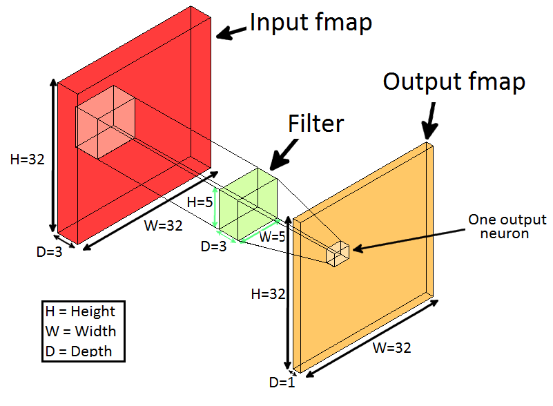
Convolutional layers use filters, which simply are three-dimensional collections of weights. The height and width of filters can vary in size ( to , e.g.), but filters typically contain weights to every layer of the input fmap. For example, if the input fmap has a depth of 3 (such as an RGB image) and the applied filter is , the filter will contain a collection of (75) weights. Applying the filter at one position produces one neuron of the output fmap. The application of the filter is identical to the calculation of (and subsequently ) in a fully-connected layer, except that the weights cover only a subset of the input neurons in this case.
To be more specific, the filter is positioned on top of the input fmap, overlapping a subset of the neurons, where each weight multiplies the neuron it overlaps with. The sum of these products, , is then used as input to some non-linear function, in the same way as in fully-connected networks. Fig.1 shows an example. Producing one layer of the output fmap entails repeating this procedure (by moving the filter over the input fmap) to generate an output neuron at each position. Using multiple filters in a similar fashion produces multiple layers of the output feature map.
The stride – the distance the filter moves by to calculate the next neuron in the output fmap – and whether the filter is permitted to slide over the edges of the input fmap, determine the height and width of the output fmap. If the stride is equal to 1, and the filter is allowed to slide over the edges of the input fmap, the output fmap becomes of the same height and width as the input fmap. To allow the filter to slide over the edges, typically the input is 0-padded, i.e., any weights that lie beyond the input fmap boundaries are multiplied by 0.
Pooling layers down-sample fmaps. In a pooling layer, the fmap is divided by width and height into multiple sections. A typical pool size would be . The largest value in each section (in each layer) is kept and the rest discarded. Thus, each section reduces to a single neuron. A pool size of decreases the height and width by a factor of . Since pooling applies to all depths of the fmap, the depth remains unchanged.
Reducing the bit precision is a common technique to improve NN efficiency. At the extreme lies binarization, where representations for all neurons and weights reduce to only one bit (Courbariaux et al., 2016). This greatly simplifies hardware complexity. In standard NNs, most of the operations comprise high latency and power hungry multiply-and-accumulate (MAC), where the values of neurons are multiplied with the values of weights, which are then summed and transformed non-linearly (typically via application of sigmoid function). For binary NNs, bit-wise XNOR operations replace multiplications. The resulting bits are then summed and compared to a threshold value. Due to their simpler nature, these operations all can be performed much more quickly and energy efficiently. Note that this applies only to forward propagation. Inference consists entirely of forward propagation and thus can fully exploit these benefits. When training, additional non-binary parameters must be maintained and updated. We focus on inference in this work and assume that training is performed offline in software. That said, training can also benefit from more efficient forward propagation as enabled by PIMBALL.
2.2. Spintronic Processing In Memory (PIM)
Without loss of generality, PIMBALL uses Computational RAM (CRAM) as the spintronic PIM substrate (Chowdhury et al., 2018). The structure consists of an array of magnetic tunnel junctions (MTJs) and can be used as a standard STT-MRAM memory array. The similarity of PIMBALL to MRAM gives it some advantages over other PIM technologies. Due to desirable properties of MTJs, the memory is fast, low power, high density, and non-volatile. Due to non-volatility, standby power is near zero. At the same time, MTJs are inherently compatible with logic operations. This enables computation to take place entirely inside the memory array, without the use of external logic or sense-amplifiers. This provides true PIM capability. Further, the structure of the array allows for massively parallel computation. As we will detail in Section 3, however, the basic array structure from (Chowdhury et al., 2018) cannot support BNNs. Building upon this limited basic design (Chowdhury et al., 2018), a key contribution of our work is novel cell and array architectures enabling efficient BNNs in memory.
The magnetic tunnel junction (MTJ) is the key building block of the memory cells. MTJs are resistive memory devices, characterized by two distinct resistance levels to represent logic 1 and logic 0. Each MTJ has two magnetic layers, a fixed layer and a free layer. The polarity of the free layer can change but the fixed cannot. When the two layers are aligned, the MTJ is in the parallel (P) state, which is considered to be logic 0. If the magnetic layers are not aligned, the MTJ is in the anti-parallel (AP) state, which is considered to be logic 1. The MTJ has a much higher resistance in the AP state than it does in the P state. The state can be changed by passing current through the MTJ, where the direction determines the final state. We now describe the 2T1M design from (Chowdhury et al., 2018).
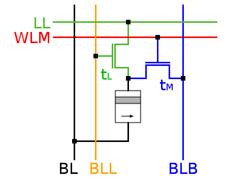
Fig.2 shows the default 2T1M cell architecture from (Chowdhury et al., 2018), which we include here as a baseline for comparison. The array formed by these cells is identical to a standard 1T1M STT-MRAM array, except for an additional access transistor per cell; the control signal Logic Line (LL) which runs along the rows; and the control signal Bit Line for Logic (BLL) which runs along the columns.
If no computation is taking place, the array based on the cell from Fig.2 can serve exactly as an STT-MRAM array. In this case, the WLM signal activates the access transistor (transistor for memory), that connects MTJs to the bitline bar (BLB) on a per row basis. Cells can then be read or written via bitline BL and BLB. The extra hardware enables computation within the array. The second access transistor (transistor for logic), connects the MTJs to the LL. BLL controls this second transistor . When BLL is activated for multiple columns, the MTJs in those columns, that are also in the same row, are connected to each other via the shared LL. MTJs that are connected over LL in a row can act either as inputs or outputs of a logic gate. Hence, the result of the logic operation changes the state of the MTJ designated as the output in place. Voltages applied to BL and BLL control the type of the logic operation. In other words, BL and BLL voltages can enforce a specific switching activity (on the output MTJ), which evolves as a function of the resistances (i.e., logic states) of the input MTJs. These voltages thereby can trigger the switching of the output MTJ according to a specific truth table. A distinct voltage range characterizes each truth table (logic gate). This structure can support different universal sets of Boolean gates and gates of various numbers of inputs (Chowdhury et al., 2018).
3. PIMBALL: BNN in Spintronic NVM
The 2T1M based design (Chowdhury et al., 2018) from Section 2.2 is limited, as any logic gate activated in a row also gets activated in all rows in the array. This is because BLL (which activates cells to serve as logic gate inputs or outputs) runs through all columns in the array. If BLL is set for a column, MTJs in that column, in all rows, get connected to LL. While such massive row level parallelism may be desirable, it impairs direct adaptation of the 2T1M design for BNN processing.
3.1. Spintronic PIM Substrate
To enable BNN, we consider two different cell (array) configurations, which range from 1T1M (one transistor per MTJ or magnet) to 3T1M (three transistors per MTJ or magnet).
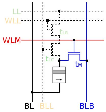
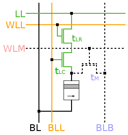
We first describe the 3T1M design. For efficient BNN processing, we need to perform computation in only a subset of the rows, while leaving all other rows unperturbed, which is not the case for the 2T1M design (Chowdhury et al., 2018). To achieve this, we can add a 3rd access transistor, as shown in Fig.3 and 3. This design preserves the very same memory interface as a standard STT-MRAM otherwise.
For logic operations, from Fig. 2 now becomes (transistor for logic column). BLL controls . The new signal Wordline for Logic (WLL) controls the third transistor, (transistor for logic row). is in series with , thus, both and must be activated to connect the MTJ to LL. This enables a row-wise and column-wise specification for any MTJ to serve as an input or output to a logic gate. BLL and WLL determine this specification. As all MTJs in a row share the same LL, still, only one logic operation can be performed in each row at a time. However, each operation can be performed in any number of the rows simultaneously. Hence, the array still features row level parallelism. We next take a closer look into memory and logic semantics.
Fig.3 shows a 3T1M PIMBALL cell activated for memory. WLM is set for only one row. This activates and connects MTJs to the BLBs. MTJs can then be read or written via voltages applied to BL and BLB. In this configuration, the array acts exactly as a standard STT-MRAM array. For data retention, i.e., if no read or write access is the case, keeping WLM, WLL, and BLL at logic 0 suffices.
Fig.3 shows a 3T1M PIMBALL cell activated for logic. WLL is set for all rows in which computation should occur. In this case we activate rows sequentially (following a similar method to Pinatubo (Li et al., 2016b)). This activates for all cells in the row. BLL is set for all columns that contain the inputs and the output. This activates for all cells in the corresponding columns. Since and are in series, only MTJs that are in cells with both activated get connected to LL. Voltages are applied to BL and BLL then to specify the type of the logic operation.
We now describe the 1T1M design. While the 3T1M design enables selective computing in the PIMBALL array (which is not the case for the 2T1M design (Chowdhury et al., 2018)), it incurs the area overhead of an extra transistor. We next present a more area efficient alternative. By “rotating” the alignment of logic operations relative to the direction of memory operations, we can reduce the number of transistors from 3 to 1, as shown in Fig.4. Due to the “rotation” we refer to this design as transposed. The two MTJs from Fig.4 are in adjacent cells in the same column. BL and BLB are replaced with Bitline Even (BLE) and Bitline Odd (BLO). Adjacent MTJs are connected to different bitlines in this case, BLE and BLO, respectively – BLO and BLE alternate throughout the entire column. Logic Line (LL) serves both as the connection between MTJs for logic operations, and also as input for read and write operations. Wordline (WL) controls the single access transistor in each cell, and is used to connect the MTJ to LL.
When no computation takes place, performing memory operations entails first setting WL. Specifically, WL gets activated for only one row. This activates the access transistors and connects MTJs (in the respective row) to LL. Voltages can then be applied to LL and either BLE or BLO (depending on the parity of the respective row) for read and write operations. When compared to the baseline 2T1M design from Fig.2, for memory access, LL and either of BLE/BLO can be thought of being equivalent to BLB and BL, respectively.
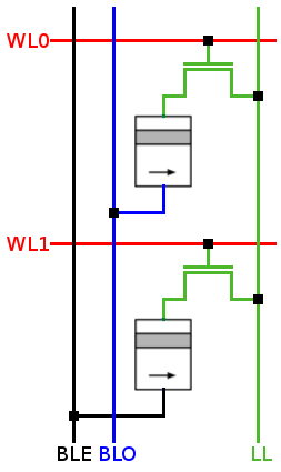
For logic on the other hand, WL is selectively set in multiple rows which connects multiple MTJs in a column to LL. This creates a connection between all activated MTJs that are in the same column. Voltages are applied to both BLE and BLO in the columns where logic gate inputs and outputs reside. These voltages determine the type of logic gates performed, following the same basic principle as 2T1M (Chowdhury et al., 2018) and 3T1M designs.
This design has the extra restriction that inputs must be in rows that are all connected to the same type of bitline (i.e., either all to BLE or all to BLO exclusively) with the output connected to the other type: If all inputs are connected to BLE (BLO), the output must be connected to BLO (BLE). This is because, following the basic logic operation principle from (Chowdhury et al., 2018), all input MTJs must be in parallel with each other and in series with the output MTJ, when it comes to forming logic gates – i.e., to enforcing switching on the output MTJ as a function of the logic states (resistances) of the input MTJs. This may impact data layout, depending on the algorithm being mapped to the array. However, the effect is negligible in most operations, including the entire implementation of BNNs. Due to the reduction to one transistor, the resulting array has nearly the same density as a standard STT-MRAM array. This is significant as density is a key advantage of STT-MRAM.
We will next look into basic computational BNN building blocks and data layout in the PIMBALL array along with design optimizations. Without loss of generality, in the following, we will use the 3T1M PIMBALL as a running example. Transposed 1T1M PIMBALL simply rotates the sense of logic operations to occur in columns rather than in rows, and is logically equivalent to 3T1M.
3.2. Computational Building Blocks
By construction, PIMBALL can perform any logic gates that CRAM can perform (Chowdhury et al., 2018), as the principle for gate formation and logic operation is the same in spite of the differences in cell and array architectures. This translates into a universal set of gates including NOT, NAND, NOR, AND, OR, and MAJ(ority). The number of inputs is arbitrary but limited by voltage variation (Sect.1). The operating principle is as follows, irrespective of the cell type: First, all MTJs (or magnets) to serve as either input or output of the logic gate being formed are connected to each other. The logic states correspond to the resistance levels of participating magnets. This always renders the same topology of a resistive network: all input magnets in parallel, connected in series to the output magnet. Voltage applied on the respective bitlines, to set the gate type , forms a voltage differential across this resistive network. The magnet corresponding to the gate output is preset to a known value. forces the gate output to switch or preserve its value as a function of the state of the inputs, according to the truth table of . More specifically, (along with the state, i.e., resistance levels of the input magnets) determines the current through the output magnet, which results in switching if this current exceeds the switching threshold.
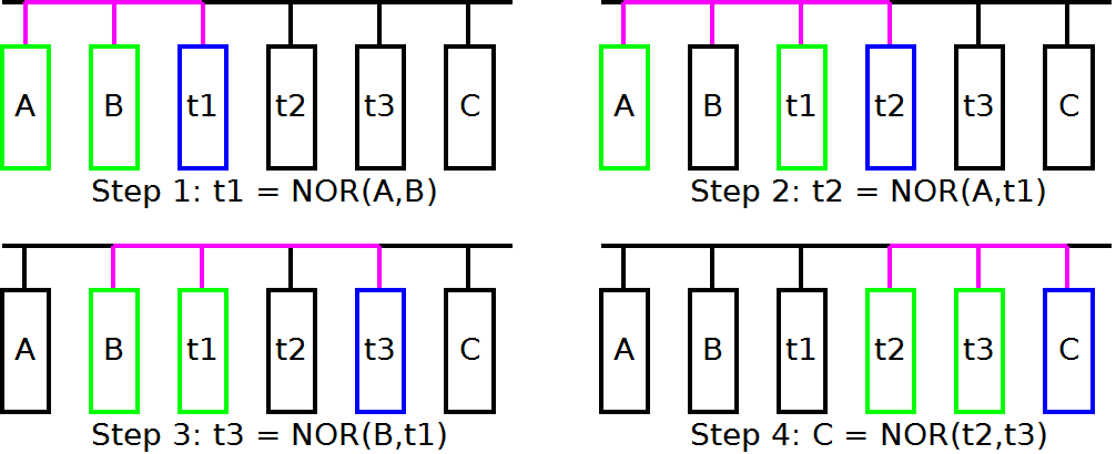
XNOR is a critical component of binarized NN implementations. The output of XNOR is 1 when the inputs are the same, and 0 otherwise. PIMBALL cannot support XNOR operation in a single step (following the resistive divider based principle). However, PIMBALL can perform XNOR using a sequence of NOR gates, following: . This process requires four NOR gates and thus four steps to complete, in addition to three temporary values (t1, t2, t3, respectively), as shown in Fig.5. The dual implementation is also possible, using two NOT and three NAND gates.
Addition is implemented by the ripple-carry algorithm, without loss of generality, where the output is computed one bit at a time. The first step is a half add and all remaining steps are full adds, which consist of NAND and NOT gates. Each full add requires four temporary values, including the carry bit, and takes a total of 5 steps. Thus, addition of two n-bit numbers requires 5n steps and 4n temporary values. Using only NAND gates, addition takes 9n steps.
Comparison to a threshold value is a common BNN correspondent of the non-linear function from Section 2.1 for ordinary NN. We implement this by subtracting the threshold value from the input and then taking the sign of the result. The sign is equal to the inverse of the borrow out signal when subtracting the threshold from the input. Thus, we do not need to perform the actual subtraction, and we only need to compute the borrow out signal. To this end, we use the ripple-borrow algorithm where a full-subtractor is implemented for each bit of the input. However, for each bit, we do not compute the difference bit, but only the output borrow, . Given , a bit of the threshold value, and , a bit of the input, the equation for in NAND form is as follows: , where is the input borrow signal, which is set to 0 for the least significant bits. The signal generated is used as the for the next full-subtractor. This is repeated for all bits of the input. The final bit is then inverted to produce the sign bit. Computing for each bit requires one NOT gate, 4 NAND gates, and 4 temporary values. Thus, comparing two n-bit numbers takes 5n+1 steps and 5n temporary bits.
Popcount takes a list of bits as input, and produces an integer equal to the number of 1s in the list. PIMBALL implements popcount with a sequence of adds. Additions are scheduled in a hierarchical manner, following the scheme of a full adder tree. Initially there is a list of 1-bit operands. First, all bits (operands) are paired and added together to form a list of 2-bit numbers. Then, pairs of these 2-bit numbers are added to form 3-bit numbers. This process repeats until there is only one number remaining, which has a value equal to the popcount of the original list of bits. If at any point the number of operands is odd, the one extra operand is sign extended and carried over to the next step. Affine transformation enables bits that are 0 to act as -1 (Liang et al., 2018), to align with the original algorithm (Courbariaux et al., 2016). This is done by doubling (logical left shifting) the final popcount result and subtracting from it a number equal to the number of input bits. In PIMBALL, the doubling operation can be done automatically by storing the result pre-shifted and the subtraction can be embedded in the subsequent thresholding operation. Thus, the transformation creates no additional overhead.
Batch Normalization primarily serves accelerating training but can also improve accuracy during inference. Batch normalization consists of a scale (multiply) and a shift (add) transformation. In the context of BNNs, it is applied to the result of the popcount before thresholding occurs. Shift-Based batch normalization (which simply replaces the costly multiplication with a shift) incurs a negligible accuracy loss (Courbariaux et al., 2016; Liang et al., 2018) and works particularly well in PIMBALL: The shift operation consists simply of writing 0s in the appropriate locations, which overwrite either the most or least significant bits of the input. No data transfer is necessary. Then, addition proceeds as described above. Other networks (Umuroglu et al., 2017) implement the same effect by thresholding and a modification of the input weights. XNOR-Net (Rastegari et al., 2016), on the other hand, uses standard batch normalization.
3.3. BNN Data Layout

In fully-connected forward propagation, each neuron has as inputs all neurons in the previous layer. Hence, for each neuron in the layer, there is a set of weights to every neuron in the previous layer. PIMBALL uses data duplication to compute each neuron in the output layer in parallel, as follows: We group one or more rows together and dedicate them to computing one neuron in the output layer. Such grouping exploits row-level parallelism at a finer granularity, i.e., in computing each output neuron. Each group of rows contains a copy of every neuron in the previous layer and all weights to those neurons. For example, when computing forward propagation from a layer with neurons to a layer with neurons, there are groups of rows, each of which contain neurons and weights. Each group also stores any necessary bits for batch normalization and thresholding, and computes in parallel.
The optimal group size , i.e., the number of rows in each group, depends on the network layer sizes. Larger increases parallelism but introduces extra overhead due to communication between rows. This is because the results from each row within a group must be moved to a single row in order to compute the final result. The number of extra data transfers required increases with group size.
Fig.6 provides an example layout where each group is a single row (). The input is layer 0; the output, layer 1. Each of the input neurons are duplicated on rows. The neurons are then XNORed with the corresponding weights, where the results overwrite the input neurons (as a space optimization). These bits are summed next (popcount), modified by batch normalization, and finally thresholded. All neurons of the computed layer are then stored in a single column (as demarcated by Output Neurons in Fig.6). The output neurons can be either the final output (if corresponding to the last layer), or inputs to the next layer of the network.
In 3-dimensional convolution, a filter is a 3-dimensional collection of weights. Filters can have different heights (y dimension) and widths (x dimension), but all filters have weights to all layers (which comprises the depth, z dimension) of the input fmap (Sect.2.1). In other words, the depth of the filter must be the same as the number of layers (depth) of the input fmap. Each filter generates one layer of the output fmap. Thus, there are as many layers in the output fmap as there are filters.
To compute the value of an output neuron, each weight (a single bit for BNN) of a filter is XNORed with a neuron in the input (also a single bit). The number of 1’s resulting from these XNOR operations are then counted. This sum is next batch normalized and thresholded, to render the bit value of the output neuron. The filter is then slid (in the x and y dimensions) over the input and an output neuron thereby is computed at each position.
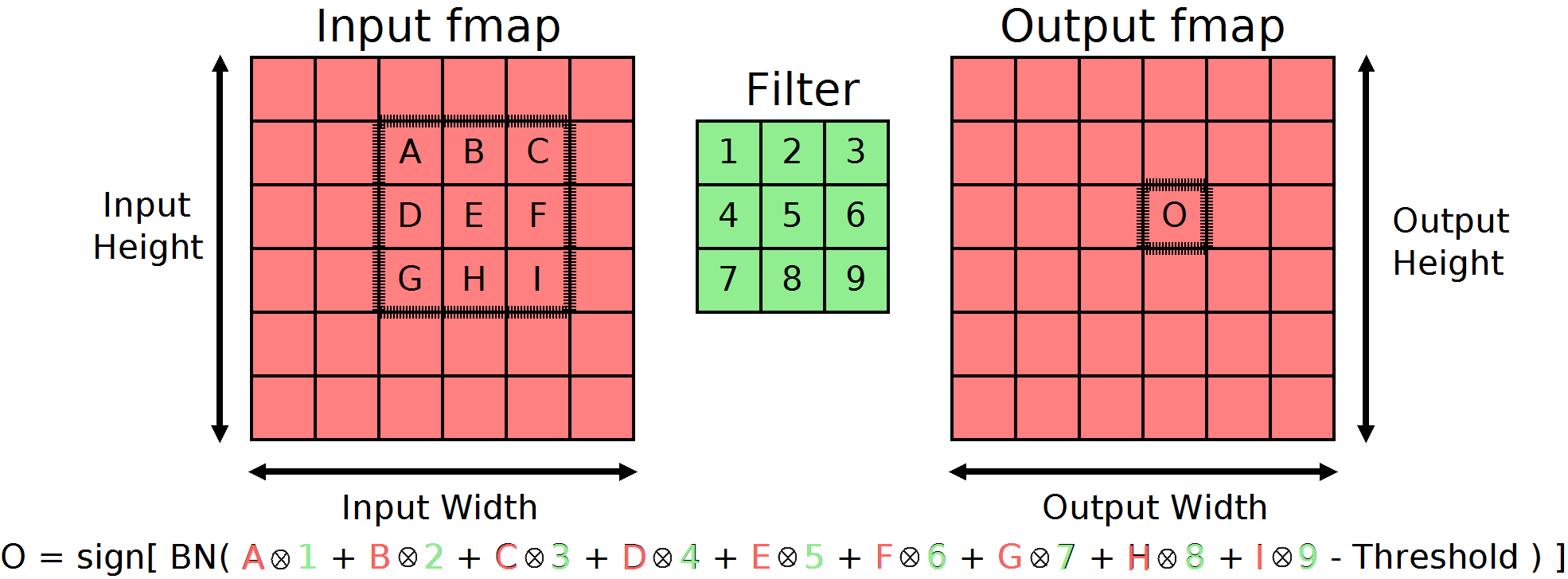
Fig.7 depicts an example, where the z dimension (depth) is 1. To compute the output neuron labeled O, each filter bit is XNORed with the input neuron it is overlapping (filter bit 1 with neuron A, filter bit 2 with neuron B, …). Fig.8 provides an example of 3-dimensional convolution with depth=2. In this case, neurons and weights at consecutive depths are stored in consecutive cells in the PIMBALL array.
Output neurons can be computed in parallel as they are not data dependent. Computing output neurons in parallel in PIMBALL requires data duplication. As is done for fully-connected layers, rows are grouped together and each group computes one output neuron. Any input neurons needed for the computation are written into the same group of rows, along with bits for the filter, batch normalization, and thresholding. Thus, each group contains all required data and can operate independently from all other groups.

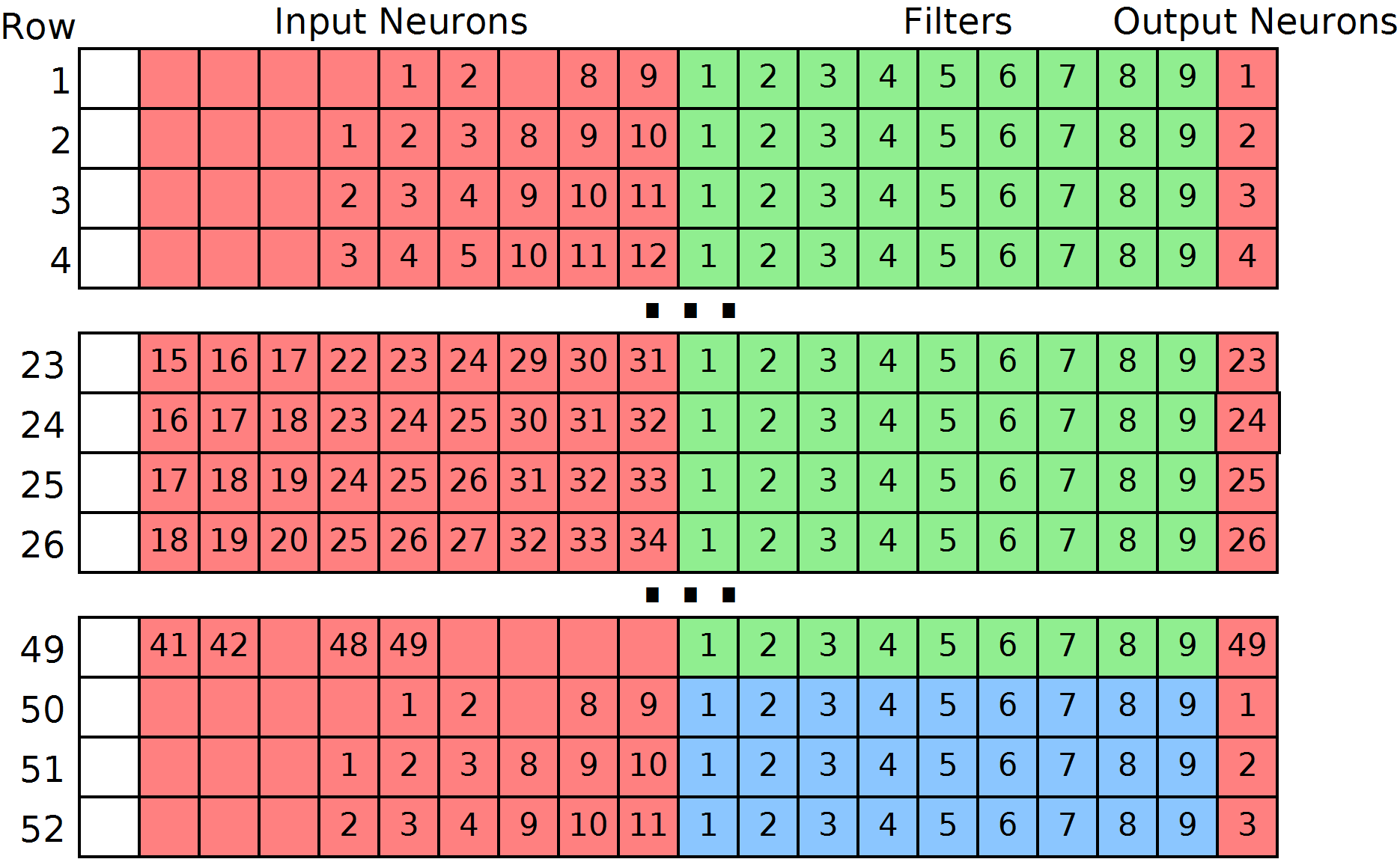
Fig.9 shows an example 2-dimensional (771) input layer along with two 2-dimensional (33) filters. Fig.10 captures the placement of these bits in the PIMBALL array, for a group size of 1 (i.e., each row computes one output neuron).
Since the filter is 33 and the input is 1 layer deep, there are 331 = 9 filter bits. All 9 of the bits of each filter are written into a single row (in the Filter Bits portion of the PIMBALL array from Fig.10). They are then duplicated across the rows so that each output bit being computed has its own copy.
In Fig.10, each row of filter bits on rows 1-49 are all the same and contain the bits for the first Filter (Fig.9(b)). The second filter is duplicated (Fig.9(c)) on rows 50-99. If there were additional filters, they would be written in the same manner on the following rows. The 9 filter bits can overlap with up to 9 input neurons, and which neurons these are depends on the specific position of the filter.
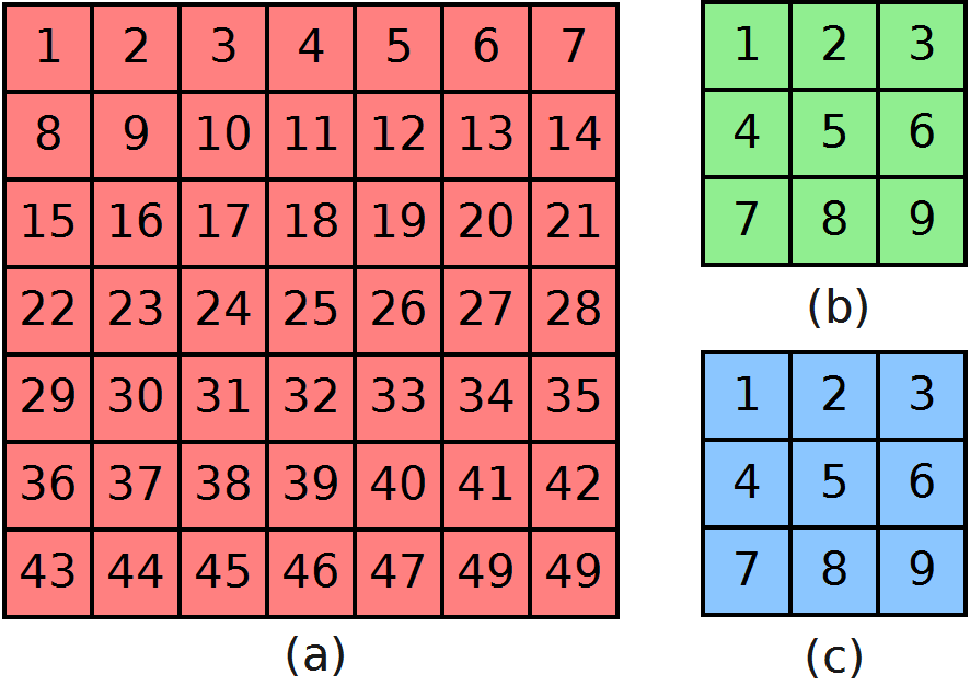
The input bits that the filter overlaps at each position are written to separate rows. Thus, there is a row for each possible position of the filter and each position of the filter is computed simultaneously. Since all filters are applied to the same input neurons, the input bit pattern must be repeated for each filter. For example, in Fig.10, row 1 is repeated on row 50 for the computation of the 2nd filter. Row 2 is repeated on row 51, and so on. Note that the filter can go over the edge of the input fmap. For example, the 33 filter centered at input neuron 1 will only overlap input bits 1, 2, 8, and 9 (as captured by rows 1 and 50). Thus, the remaining 5 locations of the 9 locations allocated for the input bits are left empty. These are filled with dummy 0’s.
As computation in each row is independent, XNOR, addition, batch normalization, and thresholding operations can be performed in parallel for all output bits of every filter. At the end of these steps of computation, all output bits are stored in a single column. The example is 2-dimensional for clarity, however, this layout easily extends to 3-dimensional convolution. If the input is z layers deep, each input and filter bit becomes an array of z bits stored in consecutive cells. For k by k filters, each group of rows contains kkz input and filter bits in this case.
3.4. Computation vs. Communication Trade-off
The fully-connected and convolutional layer organizations we covered so far locate the output neurons in a single column. For non-transposed PIMBALL arrays this is a bottleneck as each bit must be read out sequentially. One solution is sequentializing computations, by computing not all, but only a subset of the output layer neurons in parallel. For fully-connected layers, this translates into a chosen subset of the output layer neurons being computed in parallel; for convolutional layers, a subset of the filters. This leads to less data duplication. At the same time, we can store the results of each sequential step in separate columns, increasing the parallelism at which they can be read out.
4. Evaluation Setup
4.1. System Configuration
| Parameter | Modern (M) | Future (F) |
| MTJ type | Interfacial perp | Interfacial perp |
| Material system | CoFeB/MgO/CoFeB | CoFeB (SAF)/MgO/CoFeB |
| MTJ diameter | 45nm | 10nm |
| TMR | 133% | 500% |
| Threshold current | (Saida et al., 2016) | 111Through decrease of the damping constant of ferromagnetic materials (Sato et al., 2014; Mizukami et al., 2009; Dürrenfeld et al., 2015) and adopting a dual-reference layer structure (Diao et al., 2007; Hu et al., 2015) switching currents of are predicted to be possible. We assume to be conservative. |
| Switching time | 3ns (Saida et al., 2016) | 1ns |
| RP | 3.15K | 7.34K |
| RAP | 7.34K | 76.39K |
Technology Parameters: While MTJs manufactured today are capable of being used effectively in PIMBALL arrays, they are expected to significantly improve in the coming years. We therefore consider both a modern day and a projected future MTJ specification, listed in Table 1. The threshold current, , is the current at which the MTJ has a 50% chance of switching within the switching time . By setting the write current to 1.5, switching occurs with a probability of error less than .
Voltage Signature per Logic Gate: The switching activity of each logic gate output depends on the current though the output MTJ. This current in turn is a function of the voltage applied on the bitlines and the inputs – i.e., the states or resistances of the MTJs which form the gate inputs. The applied voltage directly determines the type of the gate. In other words, the voltage acts as a signature for the gate type. Therefore, correct operation demands preventing potential voltage variation on the bitlines (due to, e.g., manufacturing imperfections) from making one gate act as another gate.
| Modern (M) | Future (F) | |
|---|---|---|
| NOT | 336 (168) | 172 (191) |
| NAND | 243 (59) | 112 (82) |
| NOR | 202 (25) | 64 (13.6) |
| IMAJ-3 | 186 (15.9) | 61 (11.0) |
| IMAJ-5 | 161 (5.7) | 56 (3.8) |
The voltage signature of a gate is not restricted to a single value, and can assume any value in a gate-specific range, as shown in Table 2 for PIMBALL gates. The values in the parentheses capture the range. The parallel combination of the input MTJ resistances, in series with the output MTJ resistance, determine the voltage range. Any voltage in this range facilitates the switching activity of the output MTJ according to the truth table of the respective gate, for all input combinations. Each of these voltage ranges can be interpreted as a gate-specific voltage margin: Correct operation is guaranteed, as long as any fluctuation renders a voltage within the range corresponding to the respective gate.
The parasitic resistance of the access transistors can also affect the voltage signature and margin of the logic gates. The effect on the signature can be accounted for at design time, i.e., the voltage signature can be set depending on the expected resistance of the transistors. This is because the expected resistance is technology dependent and remains constant for each operation. Regardless of the operation, there is always one (two) transistors in between each MTJ and the logic line for the 1T1M (3T1M) design. This enables the setting of the proper voltages on the bitlines to drive the operations. What could be problematic is fluctuations of threshold voltage due to process variation, which could change the transistor resistance and consequently narrow the voltage margin. As the transistors can only add resistance, the only pathological case is if the resistance is sufficiently high to prevent switching. Fortunately, the anticipated transistor resistance, , is significantly smaller than MTJ resistances listed in Table 3. This makes logic gates relatively immune to transistor parasitic resistance. For example, the parasitic resistance would have to be 700 (15,000) for modern (future) devices in order to cause incorrect operation of a NAND gate. The large voltage margin seen for two-input gates and the high resistance values of the MTJs lead us to conclude that logic operations are robust to parasitic transistor resistance and process variation.
| Input State | Modern (M) | Future (F) |
|---|---|---|
| R11: 2 AP, 0 P | 6820 | 50900 |
| R01=R10: 1 AP, 1 P | 5354 | 23590 |
| R00: 0 AP, 2 P | 4725 | 19050 |
NAND and NOR are 2-input; inverted majority IMAJ-3 and IMAJ-5 are 3- and 5-input gates, respectively. As Table 2 indicates, generally, gates with larger fan-in have smaller margin. The reason is twofold: First, more input resistances in parallel have a smaller combined resistance. Thus, smaller changes in voltage cause a larger change in current. Second, differences in resistance between different combinations of inputs is smaller. This effect is made worse by the fact that the combined input resistance is in series with the output resistance (which is always the case, independent of the number of inputs). Hence, there is a sharp drop in voltage margin with increasing number of inputs.
It is noteworthy that NAND has a larger margin than NOR. Table 3 depicts the combined input resistance (for all possible input combinations) for 2 inputs. Recall that an MTJ in Anti-Parallel (AP) state incurs a higher resistance than in Parallel (P) state. The resistance in AP state (RAP) corresponds to logic 1; in P state (RP) , logic 0. R R01 = R R11 applies, where R00 captures the combined input resistance for the input combination 00; R01, for 01, and so on. For a given gate (hence voltage signature), the current through the output magnet, , assumes its maximum for the lowest value of the combined input resistance, hence I I01 = I I11 applies. Let us assume a non-transposed PIMBALL design, without loss of generality, where the output magnet is preset to 0 to perform NAND or NOR. For NAND, the output should switch for all combinations but 11; but for NOR, for only 00. Hence, it is critical for NAND to differentiate between R11 and R01 (= R10); for NOR, between R00 and R01 (= R10). As Table 3 indicates, the difference between the combined input resistances for NAND are much larger, which renders a larger voltage margin for correct operation.
As Table 2 indicates, for current MTJ specifications, only NAND and NOT gates are practical. The voltage margin for gates with 3 or more inputs are too small to guarantee correct operation. Predicted future MTJs have a much lower switching current but a significantly larger TMR, i.e., (RAP-RP)/RP. The effect of a larger TMR is making differences in the combined resistance of different input combinations more pronounced, and thereby increasing the voltage margins. The effect of a smaller switching current is the opposite. For low fan-in gates, the TMR effect is dominant and future MTJs have a larger margin than modern MTJs, despite the lower current. For high fan-in gates, the opposite is the case. NOT and NAND gates have very large voltage margins relative to their voltage signatures. This generally applies to other gates, as well, considering future MTJs. Restricting logic operations to only NAND and NOT gates significantly reduces susceptibility to process variation. Luckily, this is a universal set of gates. Accordingly in the evaluation, we restrict operations to only NAND, NOT, and COPY.
For the array configuration, we use a tiled architecture, where each tile is a single PIMBALL array. We evaluate two different arrays sizes, 128KB, with 1024 rows and columns, and 512KB, with 2048 rows and columns. Arrays can be accessed and used for computation independently.
For modern MTJ analysis, we take latency and energy estimates for STT-MRAM array accesses from (Dong et al., 2008), scaled to our array capacity and node size. As future MTJs are still a few years from being ready for production, the exact supporting peripheral circuitry overhead is unknown. To estimate it, we scale the latency and energy estimates so that the peripheral circuitry maintains the same percentage share of each. In both cases, the peripheral circuitry is responsible for a significant percentage of the latency. This renders a close-to-worst-case analysis, without any optimization specific to PIMBALL.
While the method by which PIMBALL performs computation is different, the array structure is similar to Pinatubo(Li et al., 2016b). The demands on our peripheral circuitry are similar to (Li et al., 2016b), as well, though we do not use sense amplifiers during computation. In the case of the 2T1M design (which we include for completeness), we use an extra transistor. Given MTJs are lower power devices, the current draw remains relatively modest even during highly parallel computation. Using projections for future MTJ devices (Table 1), a PIMBALL array performing computation on every row would still consume far less current than a DRR3 SDRAM write operation (mic, [n.d.]).
Since PIMBALL requires multi-row access, we follow the approach developed in (Li et al., 2016b), where row addresses are supplied sequentially. Modifications to the local wordline driver allow these to be latched until cleared. For logic operations, where multiple rows can be activated, we assume that the rows are addressed sequentially and take into account the latency and energy of both the row activations and voltages applied to the bitlines.
As for system integration, PIMBALL can be attached to the host system as a standalone accelerator over PCIe, or be part of the memory hierarchy (which renders a similar interface to emerging hybrid memory systems featuring NVM). In any case, PIMBALL memory space is exposed to the host (e.g., over Direct Memory Access). Software would utilize PIMBALL in a similar manner as a GPU. Code written for PIMBALL must be hardware aware in order to utilize its resources efficiently. However, unlike a GPU, PIMBALL will likely be capable of storing all required inputs, making data transfers between PIMBALL and the disk relatively infrequent. If the entire memory stack is implemented in STT-MRAM, PIMBALL could comprise the entire memory, enabling computation anywhere in the memory stack.
We assume that all BNN configuration parameters including weights and thresholds are stored in the arrays prior to computation. These parameters do not change during inference. Additionally, the PIMBALL arrays have sufficient storage to hold all, along with sufficient space for temporary values. Thus, there is no need to communicate with the host during inference. Different layers of the networks are performed in different collections of PIMBALL arrays. This creates an opportunity for pipe-lining. Inference constitutes two phases: a highly parallel computation phase and a data communication and duplication phase. Thus, each layer of the implemented networks has an associated latency and energy cost for both computation and communication. The computation phase comprises logic and memory operations which move data within the arrays. The communication phase comprises data transfers between arrays, which consists of reads from the source array and writes to the destination array.
4.2. Benchmarks and Baselines for Comparison
We implement one Imagenet, two MNIST, and two CIFAR-10 classifiers in PIMBALL, and use two representative FPGA-based BNN accelerators as the baselines for comparison, FP-BNN (Liang et al., 2018) and FINN (Umuroglu et al., 2017), respectively, which achieve higher throughput and better energy efficiency than GPU-based implementations. FP-BNN (Liang et al., 2018) uses a Maxeler MPC-2000 with a Stratix V FPGA, and FINN (Umuroglu et al., 2017) is implemented on the Xilinx Zynq-7000 SoC ZC706 Evluation kit. We reproduce the same network topologies in PIMBALL 222Some networks take in non-binary inputs. We handle multi-bit precision following (Courbariaux et al., 2016), by computing bits of each significance separately, in the same manner as binary inputs. . While the supporting hardware is different, the inputs, network sizes, and operations performed are logically identical. As a result, PIMBALL results in the same output and accuracy. In other words, we perform an iso-accuracy comparison. We also implement BioNET, a BNN kernel for similarity matching in genomics on PIMBALL. To quantitatively characterize PIMBALL’s performance and energy efficiency, we use an event-driven in-house simulator.
Fully-Connected FP-BNN follows the layer configuration of (Liang et al., 2018). The model consists of 4 fully-connected layers. The input is a 2828 gray scale image with 8-bit pixels. There are 784 input neurons (each 8 bits), 10 output neurons, and three hidden layers of 2048 neurons each. The network achieves an 98.24% accuracy on the MNIST dataset.
Fully-Connected FINN, the fully-connected network in (Umuroglu et al., 2017), is slightly smaller. The input is 2828 images that have been binarized. There are 3 hidden layers, each has 1024 neurons. The output is a vector of 10 bits corresponding to the 10 output neurons. It achieves a 98.4% accuracy on the MNIST dataset.
Convolutional FP-BNN follows the configuration provided in (Liang et al., 2018). This network contains 6 convolutional layers, 3 pooling layers, and 3 fully-connected layers. Pooling layers are computed in the same arrays as the preceding convolutional layers. Data transfer between convolutional and pooling layers is considered part of the computation phase since it is intra-array communication. The input is a 3232 image with 3 channels. All filters are 33 and all pooling layers are 22 maxpool. There are 128 filters for the first two convolutional layers, 256 filters for the third and fourth, and 512 for the fifth and sixth. The output of the last convolutional layer is 8192 neurons which are input to the first fully-connected layer. There are two hidden layers of 1024 bits each and the final output layer is 10 neurons. It achieves an accuracy of 86.31% on the CIFAR-10 dataset.
Convolutional FINN, the network in (Umuroglu et al., 2017), is similar in structure. It also has 6 convolutional layers, 3 pooling layers, and 3 fully-connected layers. All filters are 33 and all pooling layers are 22 maxpool. There are 64 filters for the first two convolutional layers, 128 filters for the third and fourth, and 256 for the fifth and sixth. There are two fully-connected hidden layers that each have 512 neurons. The output is 10 16-bit neurons. It achieves and accuracy of 80.1% on the CIFAR-10 dataset.
AlexNet, following Liang et al.(Liang et al., 2018), use the XNOR-NET (Rastegari et al., 2016) configuration to perform image classification on the ImageNet dataset. It achieves an accuracy of 42.90% for top-1 and 66.80% for top-5. The network configuration is similar to that of the other convolutional networks with the majority of the operations remaining binary. However, there are a few significant differences. The weights of some layers are not binary, in which case they are processed one bit at a time. Multiplications are introduced to perform scaling after each popcount operation. Batch-normalization is performed with multiplication, instead of the shift-based method presented earlier. Multiplications are performed inside the PIMBALL array, requiring them to be performed bit-wise and thus have a relatively high latency. The network has 5 convolutional layers, 3 of which are followed by pooling layers. After convolution, there are three fully-connected layers and the final layer is 1000 neurons representing each of the 1000 classes. AlexNet is substantially larger than the previous networks, demanding a significant amount of memory. This is to be expected as it is too large to store on-chip for most hardware implementations; Liang et al.(Liang et al., 2018) rely on external memory to store the network parameters.
We introduce a customized binarized neural network, BioNET, which finds if two strings of genomic information match or not. It is used as part of a larger genetic algorithm and it achieves an accuracy of 93.4%, on average. The core operations are the same as other BNNs, however, convolution can occur in different dimensions for different layers. Additionally, the layer sizes are non-uniform, which are listed in Table 4. As this network is the first of its kind, there is no direct baseline for comparison. As Liang et al. (Liang et al., 2018) is an FPGA specifically tailored for BNNs, which significantly outperforms CPU and GPU alternatives, we use a BioNET implementation on it as a baseline. To this end, using reported layer sizes and characterization data from (Liang et al., 2018), we extract a latency and energy model for an arbitrarily sized network on the FPGA.
| Layer | Type | Input | # Filters | Filter Size | Pool Size | Output |
|---|---|---|---|---|---|---|
| 1 | Conv | 4x100x1 | 64 | 4x3 | 1x5 | 1x20x64 |
| 2 | Conv | 1x20x64 | 32 | 1x5x64 | 1x2 | 1x10x32 |
| 3 | Conv | 1x10x32 | 20 | 1x4x32 | 1x2 | 1x5x20 |
| 4 | FC | 100 | - | - | - | 40 (10-bit) |
5. Evaluation
We evaluate PIMBALL for both Modern (M) and Future (F) MTJs, per Table 1. We restrict operations to only NAND, NOT, and COPY. We consider both an ideal (I) case, where there is no additional overhead to peripheral circuity, and one with estimates for peripheral circuitry (P). Additionally, we consider two different tiles sizes, 1024x1024 and 2048x2048. As data layout is generally more optimal in the 1T design and the 3T design incurs a large area overhead, we report results only for the 1T design.
5.1. Single Inference Pass
We start the evaluation with the performance and energy characterization for a single inference pass, which translates into the processing of a single image considering FP-BNN and FINN. This reflects the time and energy required to write the input data, compute all layers, and read final output values. Tables 5 and 6 show the total latency and energy for all networks considering different configurations, along with the latency and energy of baseline FPGA implementations. We show four configurations for future MTJ devices, with and without overhead for peripheral circuitry for tiles sizes of 1024 and 2048. We show a single configuration for modern MTJ devices, as they are less competitive.
PIMBALL typically has a lower latency than the FPGA for larger benchmarks but higher latency for smaller benchmarks. However, the main advantage of PIMBALL is increased energy efficiency. It provides significant reductions in end-to-end energy consumption for all benchmarks when using future MTJ devices. Using modern MTJ devices, PIMBALL has a higher, yet comparable, energy cost to the FPGAs. Our energy advantage decreases with larger benchmarks. This is because as benchmarks get larger there are more opportunities for parallelism. We opt to aggressively exploit these opportunities, providing the previously mentioned latency advantage, however this significantly increases our energy consumption.
Peripheral circuitry has a modest energy cost but adds a significant amount of latency. Much of the latency overhead comes from the addressing required to specify the rows and columns in which computation occurs, in addition to the addressing for memory operations. Fortunately, the peripheral latency for computation can be mitigated. The rows in which computation occur change infrequently, often separated by thousands of operations. Hence, the latency required to specify the rows can be amortized. Additionally, when a logic operation is performed, it can be applied to many rows, yet the peripheral latency for initiating the computation only has to be paid once.
Using smaller array sizes decreases latency but increases energy consumption. This is because smaller arrays have smaller rows and the computation must be divided into more rows. This increases parallelism and provides better performance, as computation in each row can proceed simultaneously. However, this also introduces additional communication overheads. Computation divided into multiple rows must be combined to produce a final result. Therefore, configurations with smaller tiles must perform more total operations for the same computation, which consumes more energy.
| FPGA | F-I-1024 | F-P-1024 | F-I-2048 | F-P-2048 | M-I-1024 | |
|---|---|---|---|---|---|---|
| FPBNN XNOR-Net | 1.16e-3 (Liang et al., 2018) | 1.84e-4 | 3.08e-4 | 3.09e-4 | 5.14e-4 | 5.53e-4 |
| FPBNN CIFAR-10 | 1.3e-4 (Liang et al., 2018) | 9.21e-5 | 1.54e-4 | 1.53e-4 | 2.54e-4 | 2.76e-4 |
| FPBNN FC | 3.39e-6 (Liang et al., 2018) | 5.05e-5 | 8.48e-5 | 9.34e-5 | 1.54e-4 | 1.52e-4 |
| FINN CIFAR-10 | 2.83e-4 (Umuroglu et al., 2017) | 8.56e-5 | 1.43e-4 | 1.42e-4 | 2.35e-4 | 2.57e-4 |
| FINN FC | 2.44e-6 (Umuroglu et al., 2017) | 3.80e-5 | 6.29e-5 | 7.33e-5 | 1.21e-4 | 1.14e-4 |
| FPGA | F-I-1024 | F-P-1024 | F-I-2048 | F-P-2048 | M-I-1024 | |
|---|---|---|---|---|---|---|
| FPBNN XNOR-Net | 3.04e-2 (Liang et al., 2018) | 5.35e-3 | 5.58e-3 | 4.96e-3 | 5.17e-3 | 3.29e-1 |
| FPBNN CIFAR-10 | 2.99e-4 (Liang et al., 2018) | 3.06e-5 | 3.19e-5 | 2.86e-5 | 2.98e-5 | 1.85e-3 |
| FPBNN FC | 1.68e-5 (Liang et al., 2018) | 1.03e-6 | 1.08e-6 | 9.92e-7 | 1.03e-6 | 6.23e-5 |
| FINN CIFAR-10 | 5.34e-4 (Umuroglu et al., 2017) | 9.49e-6 | 9.90e-6 | 9.17e-6 | 9.57e-6 | 5.75e-4 |
| FINN FC | 1.45e-5 (Umuroglu et al., 2017) | 1.46e-7 | 1.52e-7 | 1.76e-7 | 1.83e-7 | 8.86e-6 |
Using the same approach as for the previously described networks, we implement BioNET on PIMBALL and report the latency and energy consumption. As BioNet is quite small, we expect the FPGA to have a significant latency advantage. Table 7 lists the results. Consistent with previous findings, the FPGA is faster but PIMBALL is more energy efficient. As the target application, gene sequencing, is not real-time, throughput is a more significant metric than latency. In the next section we show how we can achieve high throughput while benefiting from PIMBALL’s energy efficiency.
| FPGA (Liang et al., 2018) | F-I-1024 | F-P-1024 | |
|---|---|---|---|
| Latency (s) | 9.95e-8 | 4.20e-5 | 7.04e-5 |
| Energy (J) | 2.37e-7 | 1.09e-6 | 1.13e-6 |
5.2. Pipe-lining and Scaling
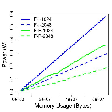
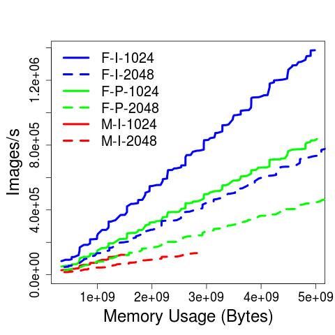
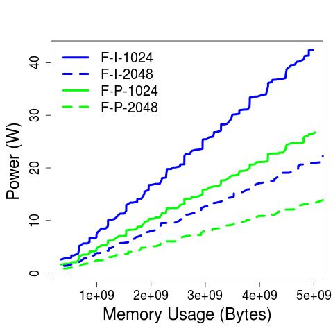
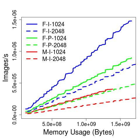
In this section we show how the scalability of PIMBALL can be used to drastically increase performance, while still taking advantage of the inherent energy efficiency of MTJ based computation. Since inference is performed across multiple arrays, an opportunity for pipe-lining exists. Once data transfer between different arrays is complete, computation in each array is independent. This allows it to proceed in parallel. Given that PIMBALL is energy efficient, many additional arrays can be added to the neural network implementations while maintaining a modest power budget.
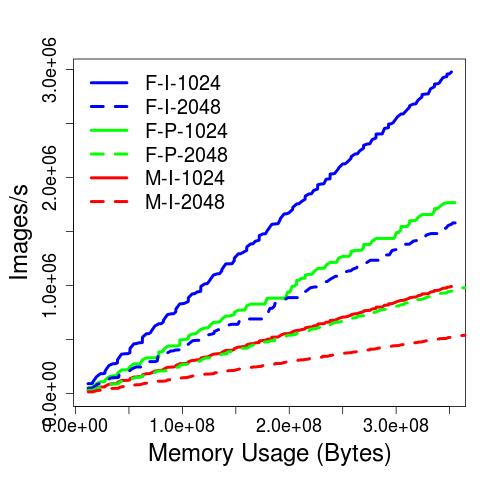
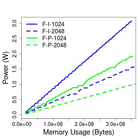
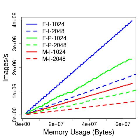
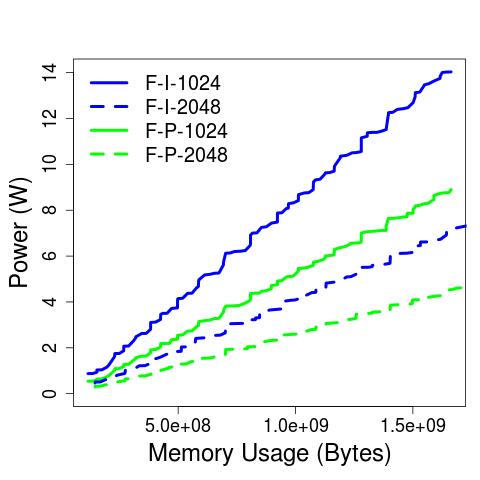
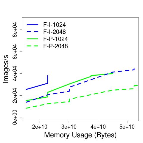
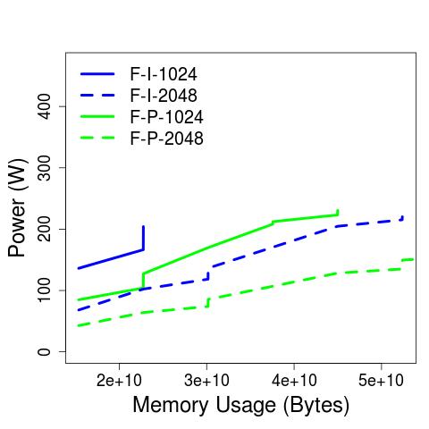
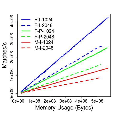
PIMBALL arrays are individual banks, many of which can reside on a single chip. Arrays that are dedicated to consecutive layers can be placed near each other to minimize the distance data must be transported. The cost of this communication is the latency and energy required to read from the source array and to write to the destination array. Since different banks can be accessed simultaneously, the destination array can be written at the same time that the source array is being read, nearly halving the latency. However, to be conservative in the estimation of the communication overhead, we assume that these memory transfers are entirely sequential.
The base pipeline configurations are those described in Sect.4, with the same number of arrays dedicated for the convolutional networks (CIFAR-10/ImageNet classifiers) and for the fully-connected networks (MNIST classifiers). However, with pipe-lining, each array can be computing a layer for a different input image at the same time. Effectively, convolutional networks are computed on a 9-stage pipeline, fully-connected networks on a 5-stage pipeline, and AlexNet on an 8-stage pipeline. Additional PIMBALL arrays can then be repeatedly added to increase performance. Each time an array is added it is dedicated to the layer that will result in an increase in the overall throughput the most. Adding PIMBALL arrays is analogous to adding ALUs to a traditional pipeline.
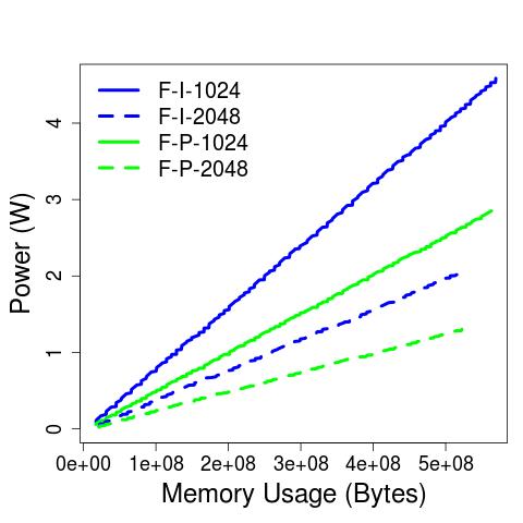
Throughput and power are reported for increasingly larger configurations . Throughput and power scale with the number of arrays, however energy per image remains nearly constant. FP-BNN (Liang et al., 2018) does not report specific throughput numbers. Their CIFAR-10 classifier is reported to have slightly less than 4 the throughput of the CIFAR-10 classifier in FINN (Umuroglu et al., 2017). Thus, we estimate the throughput of FP-BNN (Liang et al., 2018) as 4 the throughput of FINN (Umuroglu et al., 2017). The MNIST classifier in FP-BNN (Liang et al., 2018) has more neurons per layer than that in FINN (Umuroglu et al., 2017) and has additional non-binary operations. Thus, we assume that FINN provides an upper bound on the throughput of FP-BNN. For XNOR-Net, they report a latency of . A lower bound on their throughput would be 1/latency = 862 Images/sec. As XNOR-Net is too large to fit in the FPGA memory, we assume that this is a reasonable approximation.
Fig.s 12-16 depict throughput and power against memory usage for all benchmarks and configurations we considered for future MTJ devices. We report the ideal case (I), which only accounts for the latency and energy of the MTJs, and also report results accounting for the peripheral circuitry (P). This is done for both tiles sizes of 1024 and 2048. For throughput for modern MTJs, we only show the ideal case, as they are not as competitive. Due to their lack of extreme energy efficiency, power consumption for modern devices increases significantly with the introduction of pipe-lining, and thus is omitted from the figures. The PIMBALL XNOR-Net configuration is highly optimized for performance, and thus consumes significant amounts of power, even for future MTJs. We increase performance from the base configuration until the power consumption reaches , the same power consumption as the GPU implementation (Liang et al., 2018). Such aggressive performance optimization is not possible with modern MTJs, therefore we opt to reduce performance to keep the modern power budget within reason. Overall, we observe that PIMBALL can provide very high throughput while remaining at a very modest power budget. For all networks other than XNOR-Net, PIMBALL’s power budget is well below that of the FPGAs. XNORNet represents the extreme case where we heavily optimized for latency and throughput at the cost of energy efficiency. As a result, even the smallest configuration consumes a considerable amount of power. We believe that optimizing for latency is more appropriate for XNOR-Net, as the memory requirements are currently beyond the scope of edge, low-power devices. Thus, we choose to provide very high performance and consume moderate amounts of power.
While of widely varying sizes, each of the networks demonstrate similar trends. As expected, smaller tile sizes demonstrate higher throughput and higher power consumption. For a given memory usage, the configurations which consider peripheral circuitry actually have a lower power consumption. This is because peripheral circuitry has a larger effect on latency than energy. Notice also that as BioNET is not a stand-alone application but a kernel inside of a larger genomics algorithm, throughput is more valuable than latency.
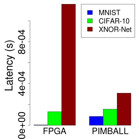
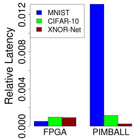
Putting it all together, the most noticeable advantage of PIMBALL is its energy efficiency. This makes it an ideal candidate for mobile applications where power consumption is critical. For example, the FP-BNN CIFAR-10 classifier which achieves an accuracy of 86.31% – accounting for predicted future peripherals and reliable NAND only operations – could process 60 Images/s at a power budget of . However, PIMBALL is not restricted to such target applications. If high performance is desired, it can easily be scaled up to achieve state-of-the-art throughputs. Even at such throughputs, the power consumption remains only a few watts. Such scalability is another key advantage of PIMBALL. By doing computation in memory, large penalties for data transfers are mitigated. The capacity allows for a large number of parameters to be stored entirely on chip. These combine to make PIMBALL particularly well suited for large scale applications which operate on large volumes of data. This is reflected in the fact that PIMBALL does not provide much benefit over an FPGA for a single image inference, but is capable of a much higher throughput. This scalability can also be seen in Fig.17. The latency of PIMBALL does not increase dramatically with benchmark size (as we move from MNIST to XNOR-Net), whereas the FPGA latency (Liang et al., 2018) does. Additionally, the relative latency of PIMBALL to an NVIDIA Tesla K40 GPU decreases with increasing benchmark size, suggesting better scalability.
6. Related Work
Numerous NN accelerators have been proposed for forward propagation on traditional compute substrates. For example, DaDianNao (Chen et al., 2014) uses a multi-chip system to implement high-precision networks. Eyeriss (Chen et al., 2017) develops a data flow to improve the energy efficiency on a spatial architecture. Tetris (Gao et al., 2017) and Neurocube (Kim et al., 2016) utilize 3D stacked memories. Neurocube uses the Hybrid Memory Cube (HMC) from Micron and performs the computation within its logic layer. Programmable state machines within the HMC are responsible for data movement and program flow. Tetris (Gao et al., 2017) also uses the HMC but focuses on using the 3D memory to optimize other components. By utilizing the high throughput of the memory and moving some of the computations to the near-memory logic layers, the authors were able to dedicate more area to computational units and alleviate overheads due to data transfer. While computation still occurs external to the memory, Tetris and Neurocube reveal the bottleneck that data transfer imposes and how creating a memory-centric design can mitigate it. Many FPGA accelerators also exist (Li et al., 2016a; Qiu et al., 2016; Suda et al., 2016). FPGA accelerators capitalizing on the benefits of binarization form the most relevant subset of this rich body of work, including (Zhao et al., 2017; Umuroglu et al., 2017; Liang et al., 2018) which can achieve significantly higher throughput and energy efficiency than competing CPU and GPU based implementations. Methods to exploit redundancy in BNNs to increase performance on FPGAs was presented in (Fu et al., 2018). SRAM based acceleration is proposed in (Eckert et al., 2018). However, by definition, SRAM cannot support large data sets. A software-reconfiguralbe accelerator for binarized neural networks intended for use with micro-controller systems was proposed in (Conti et al., 2018). They can implement small networks on-chip but must rely on external memory for practical networks. A recent paper (Kim et al., 2019) modifies XNOR-Net to use NAND operations instead and implements accelerators in DRAM and SRAM. A hybrid design was proposed in (Lee et al., 2017), where they trade off accuracy for increased energy efficiency by implementing a significant portion of the network with stochastic computing. The authors of (Nurvitadhi et al., 2016) implemented fully-connected layers of BNNs on multiple platforms, including a CPU, GPU, FPGA, and ASIC. They were able to demonstrate quantitative benefits of batching and binarization and improvements due to hardware acceleration.
When it comes to in- or near-memory NN acceleration using non-volatile memory, RRAM represents the most common substrate: RRAM, like STT-MRAM, is a resistive memory technology, where the state of a cell is stored in the resistivity of the material. Notably, RRAM has multiple resistive states and the extreme ends demonstrate a higher TMR than STT-MRAM. However, RRAM suffers from degradation with use. The state can be switched only a limited number of times before the device begins to fail.
A few reduced precision and binary neural networks have been implemented in RRAM. These networks usually take on a different form than the structure proposed in this work. RRAM accelerators typically store the weights of a network in a crossbar. The inputs (neuron values) are the voltages applied to the wordlines. The outputs of the operations are the currents on the bitlines, which are sent to an ADC (analog to digital converter) for multi-bit precision networks or a sense amplifier for binary networks. Most implementations rely on external digital logic circuits for a significant amount of the computation, such as the addition and thresholding. Thus, the RRAM crossbar is typically used just as an accelerator for the matrix-vector multiplications. This is in stark contrast with PIMBALL where all operations are performed within the memory array itself.
As representative examples, convolutional MNIST classifiers were proposed in (Yu et al., 2016) and (Xia et al., 2016). In (Xia et al., 2016), the authors binarized the output from the RRAM crossbar to avoid using ADCs and used inputs as selection signals to avoid using DACs (digital to analog converters). This was significant as ADCs and DACs typically consume the majority of energy and power in convolutional RRAM networks. Many networks were implemented this way, where the most energy efficient network (that was as accurate as the networks evaluated in our study) achieved an accuracy of 98.47% at . A similar approach was also used in (Tang et al., 2017) to classify MNIST and ImageNet data.
On the other hand, the design from (Sun et al., 2018) implements the fully-connected layers of a convolutional neural network. They activate multiple wordlines simultaneously, use two columns storing complementary weights, and a sense amplifier to compare the difference in current between two bitlines. This allows multiplication, pop-count, and thresholding to occur at the same time within the array, and removes the need for an external adder and comparator. Their network has two 64 neuron layers followed by a 10 neuron output layer. A PIMBALL implementation of this same network would be slightly more energy efficient, if peripheral circuitry overheads could be minimized. Considering practical overheads due to modern peripherals, however, PIMBALL becomes less energy efficient and considerably slower.
That said, covering only fully-connected layers, the advantage of this RRAM design (Sun et al., 2018) can only exist for small networks. Increasing the input size degrades the accuracy. Scaling to the networks evaluated in our study, which are multiple orders of magnitude larger, would make a direct implementation of the analog computing approach of this RRAM design impossible. At the same time, it is subject to errors and noise due to the analog nature of computing, which may not always be masked by the implicit noise tolerance of NN. In fact, as recent work (Feinberg et al., 2018) has demonstrated, NN on similar RRAM arrays may suffer from significant accuracy loss due to noise.
Other spintronic substrates featuring computation capability within the memory array also exist: Pinatubo (Li et al., 2016b) proposes an architecture to do general bit-wise operations in non-volatile memory. The authors in (Angizi et al., 2018) use an MTJ subarray as part of an accelerator for low bit-width convolutional NN. Recent work also covers multi-level MRAM cells to implement BNN (Pan et al., 2018). Networks with binary weights utilizing STT-MRAM were proposed in (Angizi et al., 2019). Contrary to PIMBALL, all of these platforms use sense amplifiers to perform computation. In addition, all use additional digital logic circuity. Pinatubo (Li et al., 2016b) embeds digital logic circuits into the memory for inter-subarray computation. The authors in (Pan et al., 2018) use an auxiliary processing unit to perform batch-normalization, multiplication, and pooling. The design in (Angizi et al., 2018) performs operations such as bit counting, summation, quantization and batch normalization external to the array. This is contrary to PIMBALL, which contains no additional digital logic circuitry and which performs all layers of the network entirely within the memory array. Another recent paper (Gupta et al., 2018) proposes MTJ based computation without sense amplifiers in a crossbar topology. As opposed to (Gupta et al., 2018), PIMBALL can support true PIM semantics at scale: effectively, a PIMBALL array is not any different than STT-MRAM when not used for computation. Pinatubo (Li et al., 2016b) is not explicitly tailored to NN acceleration. At the same time the convolutional networks implemented in our study are an order of magnitude larger than the network proposed in (Pan et al., 2018). Our baseline spintronic PIM substrate, CRAM, was introduced in (Chowdhury et al., 2018), and evaluated for simple and very small scale (non-binary) NN (limited to a single-neuron digit recognizer and 2D convolution, specifically) in (Zabihi et al., 2018b). As we cover in Sect.2.2, this basic memory cell and array structure cannot support BNN acceleration without modification. A review of neuro-inspired computing on non-volatile memories is provided in (Yu, 2018).
7. Conclusion
In this paper, we explored the design space of binary neural network (BNN) (forward propagation) acceleration on a spintronic processing in memory (PIM) substrate. The result is a scalable, high throughput, and specifically, highly energy efficient solution, PIMBALL. We demonstrated that PIMBALL can efficiently perform all core building blocks required for BNN forward propagation such as XNOR, pop-count, batch normalization, and thresholding, entirely within PIMBALL arrays, without any need for external circuitry, be it analog or digital, to offload computation.
Our analysis revealed that the key strength of PIMBALL is energy efficiency. A single inference pass on PIMBALL can take significantly longer when compared to representative, FPGA-based hardware alternatives which belong to best performing solutions in this context. However, achieving competitive and even better levels of throughput performance in PIMBALL, while preserving the energy efficiency gains, is straight-forward. This is because PIMBALL lends itself very well to array-level parallelism – and pipe-lining computation with (relatively slower) communication – in addition to the inherent intra-array row-level parallelism. We demonstrated that a practically feasible number of PIMBALL arrays can outperform the throughput of the FPGA counterparts while consuming only a fraction of their power. This makes PIMBALL a candidate for both low power mobile and high performance computing applications.
Another key contribution of this study is novel memory cell and array architecture designs for spintronic PIM, which we incorporated in PIMBALL arrays, and which enabled efficient BNN processing. PIMBALL arrays are implicitly re-configurable, as any row in the array can participate in any kind of computation, according to the algorithmic needs of the underlying problem. Therefore, the presented PIMBALL designs can also be expanded to other acceleration problems similar in nature (in terms of computation and communication characteristics) to BNN.
References
- (1)
- mic ([n.d.]) [n.d.]. Micron TN-41-01: Calculating Memory System Power For DDR3. https://www.micron.com/resource-details/3465e69a-3616-4a69-b24d-ae459b295aae
- Angizi et al. (2019) Shaahin Angizi, Zhezhi He, and Deliang Fan. 2019. ParaPIM: a parallel processing-in-memory accelerator for binary-weight deep neural networks. In Proceedings of the 24th Asia and South Pacific Design Automation Conference. ACM, 127–132.
- Angizi et al. (2018) Shaahin Angizi, Zhezhi He, Farhana Parveen, and Deliang Fan. 2018. IMCE: Energy-efficient bit-wise in-memory convolution engine for deep neural network. In Proceedings of the 23rd Asia and South Pacific Design Automation Conference. IEEE Press, 111–116.
- Chen et al. (2015) Wenlin Chen, James Wilson, Stephen Tyree, Kilian Weinberger, and Yixin Chen. 2015. Compressing neural networks with the hashing trick. In International Conference on Machine Learning. 2285–2294.
- Chen et al. (2014) Yunji Chen, Tao Luo, Shaoli Liu, Shijin Zhang, Liqiang He, Jia Wang, Ling Li, Tianshi Chen, Zhiwei Xu, Ninghui Sun, et al. 2014. Dadiannao: A machine-learning supercomputer. In Proceedings of the 47th Annual IEEE/ACM International Symposium on Microarchitecture. IEEE Computer Society, 609–622.
- Chen et al. (2017) Yu-Hsin Chen, Tushar Krishna, Joel S Emer, and Vivienne Sze. 2017. Eyeriss: An energy-efficient reconfigurable accelerator for deep convolutional neural networks. IEEE Journal of Solid-State Circuits 52, 1 (2017), 127–138.
- Chowdhury et al. (2018) Zamshed Chowdhury, Jonathan D Harms, S Karen Khatamifard, Masoud Zabihi, Yang Lv, Andrew P Lyle, Sachin S Sapatnekar, Ulya R Karpuzcu, and Jian-Ping Wang. 2018. Efficient in-memory processing using spintronics. IEEE Computer Architecture Letters 17, 1 (2018), 42–46.
- Conti et al. (2018) Francesco Conti, Pasquale Davide Schiavone, and Luca Benini. 2018. XNOR Neural Engine: A Hardware Accelerator IP for 21.6-fJ/op Binary Neural Network Inference. IEEE Transactions on Computer-Aided Design of Integrated Circuits and Systems 37, 11 (2018), 2940–2951.
- Courbariaux et al. (2016) Matthieu Courbariaux, Itay Hubara, Daniel Soudry, Ran El-Yaniv, and Yoshua Bengio. 2016. Binarized neural networks: Training deep neural networks with weights and activations constrained to+ 1 or-1. arXiv preprint arXiv:1602.02830 (2016).
- Diao et al. (2007) Zhitao Diao, Alex Panchula, Yunfei Ding, Mahendra Pakala, Shengyuan Wang, Zhanjie Li, Dmytro Apalkov, Hideyasu Nagai, Alexander Driskill-Smith, Lien-Chang Wang, Eugene Chen, and Yiming Huai. 2007. Spin transfer switching in dual MgO magnetic tunnel junctions. Applied Physics Letters 90, 13 (2007), 132508. https://doi.org/10.1063/1.2717556 arXiv:https://doi.org/10.1063/1.2717556
- Dong et al. (2008) Xiangyu Dong, Xiaoxia Wu, Guangyu Sun, Yuan Xie, Helen Li, and Yiran Chen. 2008. Circuit and microarchitecture evaluation of 3D stacking magnetic RAM (MRAM) as a universal memory replacement. In Design Automation Conference, 2008. DAC 2008. 45th ACM/IEEE. IEEE, 554–559.
- Dürrenfeld et al. (2015) Philipp Dürrenfeld, Felicitas Gerhard, Jonathan Chico, Randy K Dumas, Mojtaba Ranjbar, Anders Bergman, Lars Bergqvist, Anna Delin, Charles Gould, Laurens W Molenkamp, et al. 2015. Tunable damping, saturation magnetization, and exchange stiffness of half-Heusler NiMnSb thin films. Physical Review B 92, 21 (2015), 214424.
- Eckert et al. (2018) Charles Eckert, Xiaowei Wang, Jingcheng Wang, Arun Subramaniyan, Ravi Iyer, Dennis Sylvester, David Blaauw, and Reetuparna Das. 2018. Neural Cache: Bit-Serial In-Cache Acceleration of Deep Neural Networks. arXiv preprint arXiv:1805.03718 (2018).
- Feinberg et al. (2018) Ben Feinberg, Shibo Wang, and Engin Ipek. 2018. Making memristive neural network accelerators reliable. In 2018 IEEE International Symposium on High Performance Computer Architecture (HPCA). IEEE, 52–65.
- Fu et al. (2018) Cheng Fu, Shilin Zhu, Hao Su, Ching-En Lee, and Jishen Zhao. 2018. Towards Fast and Energy-Efficient Binarized Neural Network Inference on FPGA. arXiv preprint arXiv:1810.02068 (2018).
- Gao et al. (2017) Mingyu Gao, Jing Pu, Xuan Yang, Mark Horowitz, and Christos Kozyrakis. 2017. Tetris: Scalable and efficient neural network acceleration with 3d memory. In ACM SIGARCH Computer Architecture News, Vol. 45. ACM, 751–764.
- Gupta et al. (2015) Suyog Gupta, Ankur Agrawal, Kailash Gopalakrishnan, and Pritish Narayanan. 2015. Deep learning with limited numerical precision. In International Conference on Machine Learning. 1737–1746.
- Gupta et al. (2018) Saransh Gupta, Mohsen Imani, and Tajana Rosing. 2018. FELIX: fast and energy-efficient logic in memory. In Proceedings of the International Conference on Computer-Aided Design. ACM, 55.
- Han et al. (2016) Song Han, Xingyu Liu, Huizi Mao, Jing Pu, Ardavan Pedram, Mark A Horowitz, and William J Dally. 2016. EIE: efficient inference engine on compressed deep neural network. In Computer Architecture (ISCA), 2016 ACM/IEEE 43rd Annual International Symposium on. IEEE, 243–254.
- Han et al. (2015a) Song Han, Huizi Mao, and William J Dally. 2015a. Deep compression: Compressing deep neural networks with pruning, trained quantization and huffman coding. arXiv preprint arXiv:1510.00149 (2015).
- Han et al. (2015b) Song Han, Jeff Pool, John Tran, and William Dally. 2015b. Learning both weights and connections for efficient neural network. In Advances in neural information processing systems. 1135–1143.
- Hu et al. (2015) G Hu, JH Lee, JJ Nowak, JZ Sun, J Harms, A Annunziata, S Brown, W Chen, YH Kim, G Lauer, et al. 2015. STT-MRAM with double magnetic tunnel junctions. In Electron Devices Meeting (IEDM), 2015 IEEE International. IEEE, 26–3.
- Kim et al. (2016) Duckhwan Kim, Jaeha Kung, Sek Chai, Sudhakar Yalamanchili, and Saibal Mukhopadhyay. 2016. Neurocube: A programmable digital neuromorphic architecture with high-density 3D memory. In 2016 ACM/IEEE 43rd Annual International Symposium on Computer Architecture (ISCA). IEEE, 380–392.
- Kim et al. (2019) Hyeonuk Kim, Jaehyeong Sim, Yeongjae Choi, and Lee-Sup Kim. 2019. NAND-Net: Minimizing Computational Complexity of In-Memory Processing for Binary Neural Networks. In 2019 IEEE International Symposium on High-Performance Computer Architecture. IEEE/ACM.
- Lee et al. (2017) Vincent T Lee, Armin Alaghi, John P Hayes, Visvesh Sathe, and Luis Ceze. 2017. Energy-efficient hybrid stochastic-binary neural networks for near-sensor computing. In Proceedings of the Conference on Design, Automation & Test in Europe. European Design and Automation Association, 13–18.
- Li et al. (2016a) Huimin Li, Xitian Fan, Li Jiao, Wei Cao, Xuegong Zhou, and Lingli Wang. 2016a. A high performance FPGA-based accelerator for large-scale convolutional neural networks. In Field Programmable Logic and Applications (FPL), 2016 26th International Conference on. IEEE, 1–9.
- Li et al. (2016b) Shuangchen Li, Cong Xu, Qiaosha Zou, Jishen Zhao, Yu Lu, and Yuan Xie. 2016b. Pinatubo: A processing-in-memory architecture for bulk bitwise operations in emerging non-volatile memories. In Proceedings of the 53rd Annual Design Automation Conference. ACM, 173.
- Liang et al. (2018) Shuang Liang, Shouyi Yin, Leibo Liu, Wayne Luk, and Shaojun Wei. 2018. FP-BNN: Binarized neural network on FPGA. Neurocomputing 275 (2018), 1072–1086.
- Manic et al. (2016) Milos Manic, Kasun Amarasinghe, Juan J Rodriguez-Andina, and Craig Rieger. 2016. Intelligent buildings of the future: Cyberaware, deep learning powered, and human interacting. IEEE Industrial Electronics Magazine 10, 4 (2016), 32–49.
- Mizukami et al. (2009) S. Mizukami, D. Watanabe, M. Oogane, Y. Ando, Y. Miura, M. Shirai, and T. Miyazaki. 2009. Low damping constant for Co2FeAl Heusler alloy films and its correlation with density of states. Journal of Applied Physics 105, 7 (2009), 07D306. https://doi.org/10.1063/1.3067607 arXiv:https://doi.org/10.1063/1.3067607
- Nurvitadhi et al. (2016) Eriko Nurvitadhi, David Sheffield, Jaewoong Sim, Asit Mishra, Ganesh Venkatesh, and Debbie Marr. 2016. Accelerating binarized neural networks: Comparison of FPGA, CPU, GPU, and ASIC. In 2016 International Conference on Field-Programmable Technology (FPT). IEEE, 77–84.
- Pan et al. (2018) Yu Pan, Peng Ouyang, Yinglin Zhao, Wang Kang, Shouyi Yin, Youguang Zhang, Weisheng Zhao, and Shaojun Wei. 2018. A Multilevel Cell STT-MRAM-Based Computing In-Memory Accelerator for Binary Convolutional Neural Network. IEEE Transactions on Magnetics 99 (2018), 1–5.
- Qiu et al. (2016) Jiantao Qiu, Jie Wang, Song Yao, Kaiyuan Guo, Boxun Li, Erjin Zhou, Jincheng Yu, Tianqi Tang, Ningyi Xu, Sen Song, et al. 2016. Going deeper with embedded fpga platform for convolutional neural network. In Proceedings of the 2016 ACM/SIGDA International Symposium on Field-Programmable Gate Arrays. ACM, 26–35.
- Rastegari et al. (2016) Mohammad Rastegari, Vicente Ordonez, Joseph Redmon, and Ali Farhadi. 2016. Xnor-net: Imagenet classification using binary convolutional neural networks. In European Conference on Computer Vision. Springer, 525–542.
- Saida et al. (2016) Daisuke Saida, Saori Kashiwada, Megumi Yakabe, Tadaomi Daibou, Naoki Hase, Miyoshi Fukumoto, Shinji Miwa, Yoshishige Suzuki, Hiroki Noguchi, Shinobu Fujita, et al. 2016. Sub-3 ns pulse with sub-100 A switching of 1x–2x nm perpendicular MTJ for high-performance embedded STT-MRAM towards sub-20 nm CMOS. In VLSI Technology, 2016 IEEE Symposium on. IEEE, 1–2.
- Sato et al. (2014) H. Sato, E. C. I. Enobio, M. Yamanouchi, S. Ikeda, S. Fukami, S. Kanai, F. Matsukura, and H. Ohno. 2014. Properties of magnetic tunnel junctions with a MgO/CoFeB/Ta/CoFeB/MgO recording structure down to junction diameter of 11 nm. Applied Physics Letters 105, 6 (2014), 062403. https://doi.org/10.1063/1.4892924 arXiv:https://doi.org/10.1063/1.4892924
- Seshadri et al. (2017) Vivek Seshadri, Donghyuk Lee, Thomas Mullins, Hasan Hassan, Amirali Boroumand, Jeremie Kim, Michael A Kozuch, Onur Mutlu, Phillip B Gibbons, and Todd C Mowry. 2017. Ambit: In-memory accelerator for bulk bitwise operations using commodity DRAM technology. In Proceedings of the 50th Annual IEEE/ACM International Symposium on Microarchitecture. ACM, 273–287.
- Suda et al. (2016) Naveen Suda, Vikas Chandra, Ganesh Dasika, Abinash Mohanty, Yufei Ma, Sarma Vrudhula, Jae-sun Seo, and Yu Cao. 2016. Throughput-optimized opencl-based fpga accelerator for large-scale convolutional neural networks. In Proceedings of the 2016 ACM/SIGDA International Symposium on Field-Programmable Gate Arrays. ACM, 16–25.
- Sun et al. (2018) Xiaoyu Sun, Xiaochen Peng, Pai-Yu Chen, Rui Liu, Jae-sun Seo, and Shimeng Yu. 2018. Fully parallel RRAM synaptic array for implementing binary neural network with (+ 1,- 1) weights and (+ 1, 0) neurons. In Proceedings of the 23rd Asia and South Pacific Design Automation Conference. IEEE Press, 574–579.
- Tang et al. (2017) Tianqi Tang, Lixue Xia, Boxun Li, Yu Wang, and Huazhong Yang. 2017. Binary convolutional neural network on rram. In Design Automation Conference (ASP-DAC), 2017 22nd Asia and South Pacific. IEEE, 782–787.
- Umuroglu et al. (2017) Yaman Umuroglu, Nicholas J Fraser, Giulio Gambardella, Michaela Blott, Philip Leong, Magnus Jahre, and Kees Vissers. 2017. Finn: A framework for fast, scalable binarized neural network inference. In Proceedings of the 2017 ACM/SIGDA International Symposium on Field-Programmable Gate Arrays. ACM, 65–74.
- Xia et al. (2016) Lixue Xia, Tianqi Tang, Wenqin Huangfu, Ming Cheng, Xiling Yin, Boxun Li, Yu Wang, and Huazhong Yang. 2016. Switched by input: power efficient structure for RRAM-based convolutional neural network. In Proceedings of the 53rd Annual Design Automation Conference. ACM, 125.
- Yu (2018) Shimeng Yu. 2018. Neuro-inspired computing with emerging nonvolatile memorys. Proc. IEEE 106, 2 (2018), 260–285.
- Yu et al. (2016) Shimeng Yu, Zhiwei Li, Pai-Yu Chen, Huaqiang Wu, Bin Gao, Deli Wang, Wei Wu, and He Qian. 2016. Binary neural network with 16 Mb RRAM macro chip for classification and online training. In Electron Devices Meeting (IEDM), 2016 IEEE International. IEEE, 16–2.
- Zabihi et al. (2018a) Masoud Zabihi, Zamshed Chowdhury, Zhengyang Zhao, Ulya R Karpuzcu, Jian-Ping Wang, and Sachin Sapatnekar. 2018a. In-memory processing on the spintronic cram: From hardware design to application mapping. IEEE Trans. Comput. (2018).
- Zabihi et al. (2018b) Masoud Zabihi, Zamshed Chowdhury, Zhengyang Zhao, Ulya R Karpuzcu, Jian-Ping Wang, and Sachin Sapatnekar. 2018b. In-Memory Processing on the Spintronic CRAM: From Hardware Design to Application Mapping. IEEE Trans. Comput. (2018).
- Zabihi et al. (2019) Masoud Zabihi, Zhengyang Zhao, DC Mahendra, Zamshed I Chowdhury, Salonik Resch, Thomas Peterson, Ulya R Karpuzcu, Jian-Ping Wang, and Sachin S Sapatnekar. 2019. Using spin-Hall MTJs to build an energy-efficient in-memory computation platform. In 20th International Symposium on Quality Electronic Design (ISQED). IEEE, 52–57.
- Zhang et al. (2015) Chen Zhang, Peng Li, Guangyu Sun, Yijin Guan, Bingjun Xiao, and Jason Cong. 2015. Optimizing fpga-based accelerator design for deep convolutional neural networks. In Proceedings of the 2015 ACM/SIGDA International Symposium on Field-Programmable Gate Arrays. ACM, 161–170.
- Zhao et al. (2017) Ritchie Zhao, Weinan Song, Wentao Zhang, Tianwei Xing, Jeng-Hau Lin, Mani Srivastava, Rajesh Gupta, and Zhiru Zhang. 2017. Accelerating binarized convolutional neural networks with software-programmable fpgas. In Proceedings of the 2017 ACM/SIGDA International Symposium on Field-Programmable Gate Arrays. ACM, 15–24.
- Zhou et al. (2016) Shuchang Zhou, Yuxin Wu, Zekun Ni, Xinyu Zhou, He Wen, and Yuheng Zou. 2016. Dorefa-net: Training low bitwidth convolutional neural networks with low bitwidth gradients. arXiv preprint arXiv:1606.06160 (2016).