Directional control of charge and valley currents in a graphene-based device
Abstract
We propose a directional switching effect in a metallic device. To such end we exploit a graphene-based device with a three-terminal geometry in the presence of a magnetic field. We show that unidirectional charge and valley currents can be controlled by the Fermi energy and the magnetic field direction in the active device. Interestingly, unidirectional transport of charge and valley is generated between two-terminals at the same bias voltage. Furthermore, we quantify the valley depolarization as a function of disorder concentration. Our results open a way for active graphene-based valleytronics devices.I Introduction
Most often, charge transport in an electronic device is reciprocal, this is, the transmission probability from left to right equals the one from right to left. This arises typically because a device described by a time-independent scattering matrix always satisfies reciprocity Büttiker (1988). However, studies in optics Leonhardt (2006); Pendry et al. (2006) and acoustics Cummer and Schurig (2007) have broken reciprocity allowing for unidirectional transport. Interestingly, the potentials originating this effect might also remain invisible to an observer analyzing the reflection on one side of the device, a phenomenon termed unidirectional invisibility Lin et al. (2011). This has flourished more recently in the context of chiral nanophotonic waveguides Petersen et al. (2014); Price et al. (2018). In electronics, in contrast, only a few studies Foa Torres et al. (2016); Dal Lago et al. (2017) have pointed out ways of emulating this effect and the potential of such one-way devices for the transport of charge, spin and even energy remains mostly unexplored.
Moreover, in materials like graphene, the electronic states close to the Fermi energy belong to one of two inequivalent pockets in momentum space called valleys Castro Neto et al. (2009); Dubois et al. (2009); Foa Torres et al. (2014). This binary spin-like degree of freedom is a center of interest. Studies span a plethora of topics, from topological valley effects Xiao et al. (2007); Yao et al. (2008); Gorbachev et al. (2014), to valley selective circular dichroism Cao et al. (2012). Valleytronics Schaibley et al. (2016); Cresti et al. (2016) is a promising field though there are still many challenges in both generating Rycerz et al. (2007); Gunlycke and White (2011); Ingaramo and Foa Torres (2016) and detecting valley polarized currents Gorbachev et al. (2014); Shimazaki et al. (2015); Li et al. (2016); Komatsu et al. (2018); Marmolejo-Tejada et al. (2017); Wu et al. (2018).
Here, we propose an active graphene-based device producing unidirectional invisibility in the transport of charge and valley. The proposed device allows to control current flow in a peculiar way: The switch-off mechanism does not rely on the gap of the device material, this is, as a transistor the current can be switched off even when the device is effectively metallic. Furthermore, the output is directional, very much as in a diode though here there is no bias voltage applied between the source and drain.
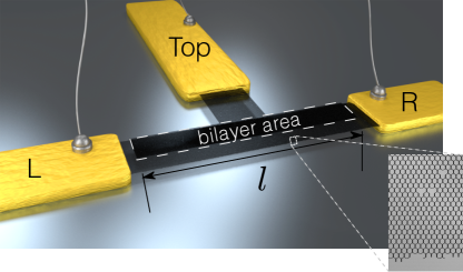
As in a transistor, our proposal uses three-terminals, that we call left (L), right (R) and top (see figure 1). Unlike a conventional field-effect transistor, the top lead generally carries a current as we show later on. In this sense, it may resemble a bipolar junction transistor but in contrast to it, here we do not obtain a current gain, but the ability to turn on or off the current in a given terminal thereby qualifying as an active device. The central part of the device is formed by a monolayer-bilayer junction threaded by a magnetic flux and connected to monolayer graphene leads on the bottom ( and ) and top () layers. In the sense of Ref. Basov et al. (2017), we use heterostructuring 111The fact that the system is a graphene bilayer is accessory, as the setup works also with a metallic 2D material on top of graphene. and high magnetic fields to achieve on-demand properties. A valley polarized current flows unidirectionally from L to R which remain at the same chemical potential. The current and valley can be inverted by tuning the Fermi energy and the magnetic field applied to the device, thereby allowing for a charge and valley switching device working at zero bias voltage.
In the following we will show how the third lead can be used as a handle to allow for one-way transport among the left and right leads. The bilayer region is used to provide a selective environment for the currents flowing through the covered edge. Essentially, the states on the top layer hybridize with those at the edge of the lower layer, thereby diverting the current from the bottom layer to the top one. This effect, however, would not be effective without the addition of a third terminal (the top one) so that the current is allowed to escape.
Now we introduce in detail our model and the simulation scheme, and our main results. Since the valley currents are expected to be specially sensitive to defects producing intervalley scattering, we also devote a section to study the valley polarization as a function of the concentration of defects in the device. Our study expand the already reach prospects for electronics based on 2D materials Fiori et al. (2014); Iannaccone et al. (2018).
II Model and method
Our simulations are based on a tight-binding model for a device as the one represented in Fig. 1. Specifically, we use a nearest-neighbors Hamiltonian with hopping eV Dubois et al. (2009); Foa Torres et al. (2014) described the Hamiltonian:
| (1) |
where and are the electronic operators for creation and annihilation at the -orbital on site , is the nearest-neighbors matrix element between sites and . models the Bernal stacking with being the matrix element between the -type atom on the top layer and the -type atom on the lower one. Additionally, includes the effect of a magnetic field applied perpendicular to the structure (by means of a Peierls substitution):
| (2) |
where is the magnetic flux quantum. To avoid reflections the magnetic field is applied to the whole device including the leads. The magnetic field is chosen so that the decay length of the edge states towards the sample is much smaller than the sample width (). In this multi-terminal case one needs to smoothly change the gauge so that it preserves the translational invariance on each terminal. To such end we use a Landau gauge following the prescription given in Ref. Baranger and Stone, 1989.
To model the bias voltage applied perpendicularly to the bilayer the on-site energies are modified, being for the lower layer and for the upper one (the same bias is applied to the corresponding leads).
The transport simulations correspond to the coherent regime, where Landauer-Büttiker theory predicts that the current at lead is:
| (3) |
where , with being the top lead, and is the Fermi-Dirac distribution at lead .
The results presented here were obtained with home-made codes built on the Kwant Groth et al. (2014) module. Two of the leads are plugged to the lower layer ( and ) and a third one () to the upper layer. In our simulations the device width () and length () are 104 ( 25 nm) and 512 ( 125 nm), respectively, and the top layer covers just of the bottom one. Furthermore edge roughness and site vacancies were added to the sample region as shown in the inset of Fig. 1. The perpendicular bias between the bottom and top of 0.4, and a magnetic field was applied perpendicularly to the device. It is important to note that these parameters were chosen for easier computation and to show the mechanism. Nevertheless, one may drastically reduce the magnetic field and with that the bias voltage to experimentally more accesible values just by using a larger sample. Finally, we would like to mention other related proposal Mahfouzi et al. (2010) involving a ferromagnet on topological insulator and another where stacking variations are used to achieve layer selectivity in transport Abdullah2016 .
III Results and discussion
III.1 Directional transport and non-reciprocal bandstructure
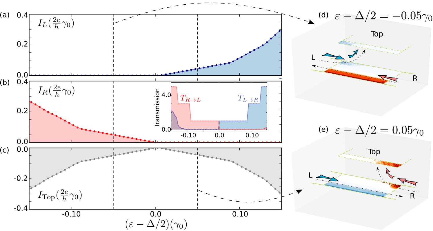
Figure 2(a-c) shows the currents on each lead as a function of the occupations set by the Fermi energy on the left and right leads (measured from , the onsite energy at the lower layer). Note that and are kept at the same chemical potential while the bias voltage with the top lead is kept at a fixed value. When the Fermi energy is set to so that the right lead has a non-zero current the left one is inactive (off) and viceversa. The origin of this sharp asymmetry can be visualized in Fig. 2(d) showing the probabilities associated to scattering states coming from the right (left) is shown in red (blue) tones. It is important to note that Fig. 2 (d) and (e) represent the scattering wavefunctions incoming from left and right leads into the bilayer-monolayer junction (the color scale is in log scale for better visualization). The positions of each lead plugged to the scattering zone has been emphasized with L, R and Top, located along the green dashed lines. The chirality of the states induced by the magnetic field separates these scattering wave-functions according to the direction of incidence, while the geometry of the top layer determines their fate: The states incident from the right lead are fully transmitted to the left lead. In contrast, those states incident from the left lead are not transmitted to the right but are neither reflected back to the left (see Fig. 2(b)-inset showing the transmission probabilities as a function of the incoming electronic energy measured from ), they are, in turn, transmitted to the top electrode. Thus, transport becomes directional, is nonzero while the lack of reflection in the left lead renders a vanishing . The opposite occurs when as seen in Fig. 2(e). Note that, as expected, the curves in Fig. 2 (a-c) are not electron-hole symmetric.
Hence, from Fig. 2 we can see that the current on or can be switched on or off by changing , even though the device always remains metallic. The on state at the left lead would be achieved when the Fermi energy is on the positive side of the horizontal axis in Fig. 2 (a), while the off state would correspond to a Fermi energy on the negative side of the horizontal axis. This is, one gets a switching effect in a metallic device. The magnitude of needs to allow for an energetic overlap between states from both layers. As decreases the on-off energy region where one way transport can be achieved also does. Taking this into account, a compromise between a satisfactory one way transport energy region and an experimentally affordable value needs to be achieved. In the following paragraphs we explore the physics behind the directional switching effect in a metal described above, we also numerically prove the valley filtering features of the proposed device and evaluate the robustness of the generated valley currents in the presence of intervalley processes.
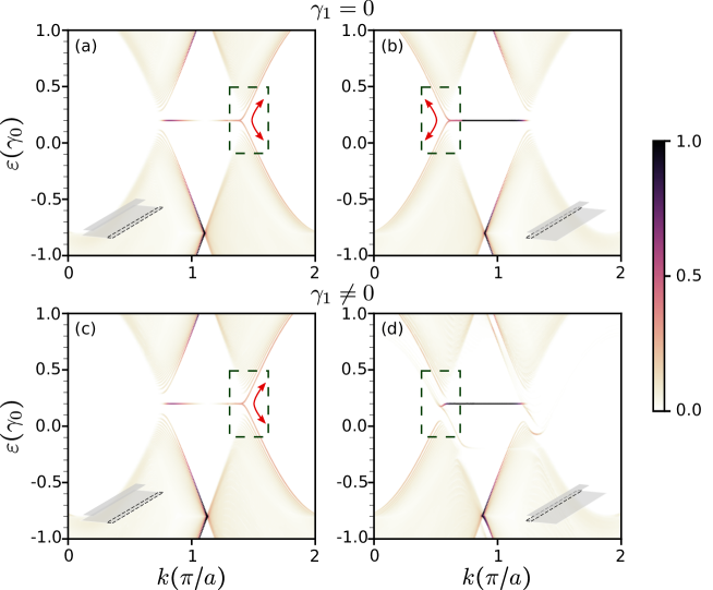
To rationalize the non reciprocal electronic transport observed in Fig. 2, we now turn to the band structure of a partially covered graphene bilayer. Specifically we will show how one can craft asymmetric propagating states under feasible experimental conditions. The four panels of Fig. 3 present the electronic dispersion weighted on the edges of the bottom layer of a partially covered “zig-zag” graphene bilayer. The color scale encodes the weight of the corresponding states on a narrow stripe of from the covered ((b) and (d)) or uncovered edge ((a) and (c)).
Panels (a) and (b) correspond to the interlayer interaction set to , while panels (c) and (d) have = 0.15 McCann et al. (2007). In these simulations the width () of the bottom layer is and the top layer covers just one fourth of the bottom one ().
Figure 3 shows the energy dispersion of a partially covered bilayer-monolayer junction with (a and b) and without the interlayer interaction. The color scale encodes the weight on a narrow stripe of 6 unit cells from the edges of the bottom layer as represented in the schemes in the insets to each panel. These unveils a peculiar effect of the interlayer interaction: the selective switch-off of the propagating state localized in the covered edge, whose absence is highlighted with a dashed rectangle (panel d). In contrast, the propagating state on the uncovered edge remains as seen in Fig. 3(c) (red arrows). Interestingly, these surviving states move in one direction without a counterpart propagating on the opposite one, and have a pseudomomentum limited to one valley.
This selective break down of the propagating state localized on the covered edge yields an asymmetrical band structure that is responsible for the non-reciprocal transport properties of the device. At this point one can compare the action of the proposed system with that of a diode. However, in contrast to a diode, our proposal works even when the bias voltage difference between and is zero, and it does not rely on the generation of charge separation in a p-n junction.
III.2 Valley filtering
As a final step we turn to the valley filtering features of the device. With this in mind, we turn to a modified device in order to quantify the depolarization of the propagating states that make their way to the exit lead (L or R), and to ascertain the persistence of this polarization to valley scatterers. To such end we consider that the magnetic field is slowly turned-off when entering the graphene leads. This provides a unambiguous definition of the valleys in the asymptotic channels. To evaluate the sensitivity of the valley polarization to defects, we randomly place vacancies over a length at each end of the device, immediately after the region where the magnetic field is turned-off. This way, we can test whether the polarization remains after traversing a region with defects and how fast is the depolarization process (note that in this configuration one can have forward intervalley processes).
For this new device scheme the scattering matrix is obtained in the normal modes base which allows to estimate the scattering probabilities connecting the propagating modes of each lead. With this information the degree of polarization of the state at each valley is computed as where and are the valleys labels and is the transmission probability summed over all the outgoing modes neighboring valley.
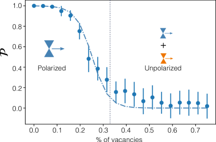
Figure 4 shows valley polarization, averaged over realizations, as a function of the vacancies concentration. One can see in absence of vacancies the state that “survives” the filtering process is perfectly polarized, as was suggested by the analysis of the band structure. Interestingly, we can note that the polarization of the outcoming states is not immediately annihilated by the presence of valley scatterers, it persists despite the presence of a considerable concentration of vacancies. The fitting of the obtained results (blue dashed line) with an hyperbolic tangent function points out that with of valley vacancies the valley polarization is . This suggests that the polarization of the outcoming currents could be experimentally measured and used as a source of valley polarized currents. These sources of switchable valley polarized states remain absent from the toolkit of nano-electronics and is the cornerstone for the expansion of valleytronic devices.
IV Final remarks
We have presented an experimentally feasible way to generate layer-polarized one-way states in an heterogenous bilayer graphene device, a building block for directional layertronics Jaskólski et al. (2018). The search of a transistor-like effect in a metal has been an outstanding issue for a long time Rotkin and Hess (2004) and one of the motivations for the discovery of graphene Novoselov et al. (2004) where the modest on-off ratios were considered to be “a fundamental limitation of any material without a gap exceeding ” Novoselov et al. (2004). In our case, the on-off ratios are expected to be comparable with state of the art transistors (with the differences pointed out in the introduction).
The proposed system may also serve as a possible source of valley polarized carriers. Interestingly, our results show that the valley polarization may stand a high concentration of defects, thereby opening interesting prospects for further research.
Author contributions. All the authors contributed to the planning of the research. MB carried out the numerical simulations and wrote a draft on the main results. LEFFT wrote a first draft of the manuscript which was improved by all authors.
Conflicts of interest. There are no conflicts of interest to declare
Acknowledgments. MB, JEBV and LEFFT acknowledge support from FondeCyT (Chile) through grants number 3170143, 3170126 and 1170917.
References
- Büttiker (1988) M. Büttiker, “Symmetry of electrical conduction,” IBM Journal of Research and Development, IBM Journal of Research and Development 32, 317 (1988).
- Leonhardt (2006) U. Leonhardt, “Optical conformal mapping,” Science 312, 1777 (2006), http://science.sciencemag.org/content/312/5781/1777.full.pdf .
- Pendry et al. (2006) J. B. Pendry, D. Schurig, and D. R. Smith, “Controlling electromagnetic fields,” Science 312, 1780 (2006), http://science.sciencemag.org/content/312/5781/1780.full.pdf .
- Cummer and Schurig (2007) S. A. Cummer and D. Schurig, “One path to acoustic cloaking,” New Journal of Physics 9, 45 (2007).
- Lin et al. (2011) Z. Lin, H. Ramezani, T. Eichelkraut, T. Kottos, H. Cao, and D. N. Christodoulides, “Unidirectional invisibility induced by -symmetric periodic structures,” Phys. Rev. Lett. 106, 213901 (2011).
- Petersen et al. (2014) J. Petersen, J. Volz, and A. Rauschenbeutel, “Chiral nanophotonic waveguide interface based on spin-orbit interaction of light,” Science 346, 67 (2014), http://science.sciencemag.org/content/346/6205/67.full.pdf .
- Price et al. (2018) D. M. Price, D. L. Hurst, C. Bentham, M. N. Makhonin, B. Royall, E. Clarke, P. Kok, L. R. Wilson, M. S. Skolnick, and A. M. Fox, “Non-Reciprocal Transmission and Reflection of a Chirally-Coupled Quantum Dot,” arXiv:1801.09958 [cond-mat, physics:quant-ph] (2018), arXiv: 1801.09958.
- Foa Torres et al. (2016) L. E. F. Foa Torres, V. Dal Lago, and E. Suárez Morell, “Crafting zero-bias one-way transport of charge and spin,” Phys. Rev. B 93, 075438 (2016).
- Dal Lago et al. (2017) V. Dal Lago, E. Suárez Morell, and L. E. F. Foa Torres, “One-way transport in laser-illuminated bilayer graphene: A floquet isolator,” Phys. Rev. B 96, 235409 (2017).
- Castro Neto et al. (2009) A. H. Castro Neto, F. Guinea, N. M. R. Peres, K. S. Novoselov, and A. K. Geim, “The electronic properties of graphene,” Rev. Mod. Phys. 81, 109 (2009).
- Dubois et al. (2009) S. M.-M. Dubois, Z. Zanolli, X. Declerck, and J.-C. Charlier, “Electronic properties and quantum transport in graphene-based nanostructures,” The European Physical Journal B 72, 1 (2009).
- Foa Torres et al. (2014) L. E. F. Foa Torres, S. Roche, and J. C. Charlier, missingtitle “Introduction to Graphene-Based Nanomaterials: From Electronic Structure to Quantum Transport” (Cambridge University Press, 2014).
- Xiao et al. (2007) D. Xiao, W. Yao, and Q. Niu, “Valley-contrasting physics in graphene: Magnetic moment and topological transport,” Phys. Rev. Lett. 99, 236809 (2007).
- Yao et al. (2008) W. Yao, D. Xiao, and Q. Niu, “Valley-dependent optoelectronics from inversion symmetry breaking,” Phys. Rev. B 77, 235406 (2008).
- Gorbachev et al. (2014) R. V. Gorbachev, J. C. W. Song, G. L. Yu, A. V. Kretinin, F. Withers, Y. Cao, A. Mishchenko, I. V. Grigorieva, K. S. Novoselov, L. S. Levitov, and A. K. Geim, “Detecting topological currents in graphene superlattices,” Science 346, 448 (2014).
- Cao et al. (2012) T. Cao, G. Wang, W. Han, H. Ye, C. Zhu, J. Shi, Q. Niu, P. Tan, E. Wang, B. Liu, and J. Feng, “Valley-selective circular dichroism of monolayer molybdenum disulphide,” Nature Communications 3, 887 (2012).
- Schaibley et al. (2016) J. R. Schaibley, H. Yu, G. Clark, P. Rivera, J. S. Ross, K. L. Seyler, W. Yao, and X. Xu, “Valleytronics in 2d materials,” Nature Reviews Materials 1, 16055 EP (2016).
- Cresti et al. (2016) A. Cresti, B. K. Nikolić, J. H. García, and S. Roche, “Charge, Spin and Valley Hall Effects in Disordered Graphene,” Riv. Nuovo Cimento 39, 587 (2016).
- Rycerz et al. (2007) A. Rycerz, J. Tworzydlo, and C. W. J. Beenakker, “Valley filter and valley valve in graphene,” Nat Phys 3, 172 (2007).
- Gunlycke and White (2011) D. Gunlycke and C. T. White, “Graphene valley filter using a line defect,” Phys. Rev. Lett. 106, 136806 (2011).
- Ingaramo and Foa Torres (2016) L. H. Ingaramo and L. E. F. Foa Torres, “Valley filtering by a line-defect in graphene: quantum interference and inversion of the filter effect,” Journal of Physics: Condensed Matter 28, 485302 (2016).
- Shimazaki et al. (2015) Y. Shimazaki, M. Yamamoto, I. V. Borzenets, K. Watanabe, T. Taniguchi, and S. Tarucha, “Generation and detection of pure valley current by electrically induced berry curvature in bilayer graphene,” Nature Physics 11, 1032 (2015).
- Li et al. (2016) J. Li, K. Wang, K. J. McFaul, Z. Zern, Y. Ren, K. Watanabe, T. Taniguchi, Z. Qiao, and J. Zhu, “Gate-controlled topological conducting channels in bilayer graphene,” Nature Nanotechnology 11, 1060 (2016).
- Komatsu et al. (2018) K. Komatsu, Y. Morita, E. Watanabe, D. Tsuya, K. Watanabe, T. Taniguchi, and S. Moriyama, “Observation of the quantum valley hall state in ballistic graphene superlattices,” Science Advances 4 (2018), 10.1126/sciadv.aaq0194, http://advances.sciencemag.org/content/4/5/eaaq0194.full.pdf .
- Marmolejo-Tejada et al. (2017) J. M. Marmolejo-Tejada, J. H. García, M. D. Petrović, P.-H. Chang, X.-L. Sheng, A. Cresti, P. Plecháč, S. Roche, and B. K. Nikolic, “Deciphering the origin of nonlocal resistance in multiterminal graphene on hexagonal-boron-nitride with ab initio quantum transport: Fermi surface edge currents rather than Fermi sea topological valley currents,” Journal of Physics: Materials 1, 015006 (2018).
- Wu et al. (2018) Z. Wu, B. T. Zhou, G.-B. Liu, J. Lin, T. Han, L. An, Y. Wang, S. Xu, G. Long, C. Cheng, K. T. Law, F. Zhang, and N. Wang, “Intrinsic valley Hall transport in atomically thin MoS2,” arXiv:1805.06686 [cond-mat] (2018), arXiv: 1805.06686.
- Basov et al. (2017) D. N. Basov, R. D. Averitt, and D. Hsieh, “Towards properties on demand in quantum materials,” Nature Materials 16, 1077 (2017).
- Note (1) The fact that the system is a graphene bilayer is accessory, as the setup works also with a metallic 2D material on top of graphene.
- Fiori et al. (2014) G. Fiori, F. Bonaccorso, G. Iannaccone, T. Palacios, D. Neumaier, A. Seabaugh, S. K. Banerjee, and L. Colombo, “Electronics based on two-dimensional materials,” Nature Nanotechnology 9, 768 (2014).
- Iannaccone et al. (2018) G. Iannaccone, F. Bonaccorso, L. Colombo, and G. Fiori, “Quantum engineering of transistors based on 2d materials heterostructures,” Nature Nanotechnology 13, 183 (2018).
- Baranger and Stone (1989) H. U. Baranger and A. D. Stone, “Electrical linear-response theory in an arbitrary magnetic field: A new fermi-surface formation,” Phys. Rev. B 40, 8169 (1989).
- Groth et al. (2014) C. W. Groth, M. Wimmer, A. R. Akhmerov, and X. Waintal, “Kwant: a software package for quantum transport,” New Journal of Physics 16, 063065 (2014).
- Mahfouzi et al. (2010) F. Mahfouzi, B. K. Nikolić, S.-H. Chen, and C.-R. Chang, “Microwave-driven ferromagnet˘topological-insulator heterostructures: The prospect for giant spin battery effect and quantized charge pump devices,” Phys. Rev. B 82, 195440 (2010).
- (34) H.M. Abdullah, M. Zarenia, H. Bahlouli, F.M. Peeters, B. Van Duppen, EPL 113, 17006 (2016).
- McCann et al. (2007) E. McCann, D. S. Abergel, and V. I. Fal’ko, “The low energy electronic band structure of bilayer graphene,” The European Physical Journal Special Topics, The European Physical Journal Special Topics 148, 91 (2007).
- Jaskólski et al. (2018) W. Jaskólski, M. Pelc, G. W. Bryant, L. Chico, and A. Ayuela, “Controlling the layer localization of gapless states in bilayer graphene with a gate voltage,” 2D Materials 5, 025006 (2018).
- Rotkin and Hess (2004) S. V. Rotkin and K. Hess, “Possibility of a metallic field-effect transistor,” Applied Physics Letters 84, 3139 (2004), https://doi.org/10.1063/1.1710717 .
- Novoselov et al. (2004) K. S. Novoselov, A. K. Geim, S. V. Morozov, D. Jiang, Y. Zhang, S. V. Dubonos, I. V. Grigorieva, and A. A. Firsov, “Electric field effect in atomically thin carbon films,” Science 306, 666 (2004), http://www.sciencemag.org/content/306/5696/666.full.pdf .