An atomically thin oxide layer on the elemental superconductor Ta(001) surface
Abstract
Recently the oxygen-reconstructed tantalum surface Ta(001)-p(33)-O has experienced considerable attention due its use as a potential platform for Majorana physics in adatom chains. Experimental studies using scanning tunneling microscopy and spectroscopy found rich atomic and electronic structures already for the clean Ta(001)-O surface, which we combine here with ab initio methods. We discover two metastable superstructures at the root of the different topographic patterns, discuss its emergence during annealing, and identify the electronic properties. The latter is determined as the sole origin for the contrast reversal seen at positive bias. The observed effects are essentially connected to the two distinct oxygen states appearing on the surface in different geometries. The second superstructure was found in simulations by introducing oxygen vacancies, what was also observed in tantalum pentoxide systems. Additionally we study the charge distribution on the oxidized surface and underline its importance for the adsorption process of polarizable atoms and molecules.
pacs:
68.43.-h, 68.47.De, 68.47.Gh, 68.43.Fg, 82.65.+r, 68.37.Ef, 73.20.HbThe surfaces of elementary superconductors have recently attracted a lot of attention due to their potential in being used as platform for chains which may host Majorana quasiparticles Nadj-Perge et al. (2014); Ruby et al. (2015, 2017); Jeon et al. (2017); Kim et al. (2018); Kamlapure et al. (2018). One requirement for the formation of Majorana states is a strong spin-orbit coupling in the magnetic chain on superconductor system which facilitates the formation of non-collinear magnetization states. Therefore, high- elementary superconductors which have an experimentally easily accessible transition temperature above are particularly interesting.
While clean Pb and Re surfaces have been explored Nadj-Perge et al. (2014); Ruby et al. (2015, 2017); Jeon et al. (2017); Kim et al. (2018), the preparation of clean Ta, La, and Nb surfaces is more challenging Eelbo et al. (2016); Titov and Jagodzinski (1985); Kuznetsov et al. (2010); Razinkin and Kuznetsov (2010) particularly due to the tendency to form O reconstructions at the surface.
On the other hand, such reconstructions also add to the functionality of the surface, as they tend to decouple the spins of adatoms from the substrate conduction electrons Heinrich et al. (2004); Hirjibehedin et al. (2007), which enables to tune the coupling of the adatom spins to the Cooper pairs Cornils et al. (2017). Ta(110) and Ta(001) have been studied by scanning tunneling microscopy (STM) Eelbo et al. (2016); Cornils et al. (2017). However, the way the structure of the O reconstruction of Ta(100) is linked to the STM images found in Ref. Cornils et al. (2017) remained elusive.
A first attempt to characterize the geometry of the Ta(001)-O surface was done by Titov et al. Titov and Jagodzinski (1985). Few simple models were proposed to verify the LEED and AES experiment, and it was shown that a couple of O atom arrangements with different coverages can appear at various temperatures. Also, a modified surface with a superimposed (33)O network was predicted. Other structures for the oxidized Ta surface were studied recently by Guo et al. Guo et al. (2017) and Bo et al. Bo et al. (2018) from an electronic and quantum-chemical point of view Sun (2014). In case of Ta(001) Guo et al. (2017), the study concentrated on O atoms adsorbed at hollow positions only, in contrast to the models proposed by Titov et al. Adsorption at low-coordinated bridge positions, however, was found relevant for bcc metals as regards reconstruction Koller et al. (2001), catalysis Brambilla et al. (2013), and CO coadsorption Zhang and Hu (2000).
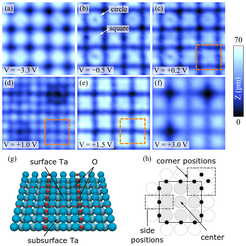
Here, we present a joint study of Ta(001)-p(33)-O by means of experimental (STM, scanning tunneling spectroscopy (STS)) and first-principles (density functional theory (DFT)) techniques. We show the interplay between two types of O positions being the reason for two distinct shapes of 33 plaquettes observed in the STM images. Charge transfer between surface sites revealed a distinct polarization texture, which, together with the electronic structure, we predict to be relevant for adsorption of other atoms and molecules.
The surface under study was prepared as described in the Supplementary Information below. To investigate local spectroscopic properties of the sample, spectra were taken using a W tip via Lock-in technique with stabilization voltage and current and , and with a modulation voltage of ( ) added to the sample bias voltage .
Fig. 1 shows STM images measured at the same location at various . From Fig. 1(b) it can be seen that oxidized Ta(001) forms a well ordered superstructure lattice where a regular network of plaquettes of square and circular shapes separated by continuous depression lines with an apparent depth of at are visible. Square-shaped plaquettes are much more frequent than circular-shaped plaquettes with a relative abundance of 4:1. The lateral distance of these plaquettes is , with the lattice constant of Ta, which reveals the 33 nature of the superstructure formation. The periodicity is consistent with the structure that has been assumed by Titov et al. Titov and Jagodzinski (1985) (see Fig. 1(g)). However, it is a priori unknown, whether the plaquettes are due to 33 Ta atoms and the depression lines are the O atoms, or vice versa, and what the reason is for the circular- and cross-shaped appearance of the plaquettes. This is further complicated by the second most important experimental result of the present study. There is a shift of the contrast by half of the distance between the plaquettes around a bias voltage of (cf. Figs. 1(c-e)).
To reveal the atomic structure in the experimentally observed 33 plaquettes, we performed DFT calculations on the (33)O superstructure on Ta(001) with the VASP package Kresse and Furthmüller (1996). For this purpose we used spin-polarized LDA+ and GGA+ functionals with enlarged cut-off energies up to , including on O atoms, that has been found relevant in oxide systems Nekrasov et al. (2000) (see Supplementary Information for details). The starting geometry was chosen as proposed by Titov et al. Titov and Jagodzinski (1985). It consists of an idealized 33 array of O atoms superimposed on the Ta(001) surface. The result of the relaxation is displayed in Fig. 2(a), and denoted as state I (Supplementary Information). The length of the 33 plaquette is estimated as = , which is consistent with the periodicity of the reconstruction observed in STM. The first interlayer spacing is compressed by in comparison to bulk values. The surface exhibits both out-of-plane and in-plane reconstruction with buckling of Ta atoms, and zigzag-ordered (along -axis) rows of O atoms.
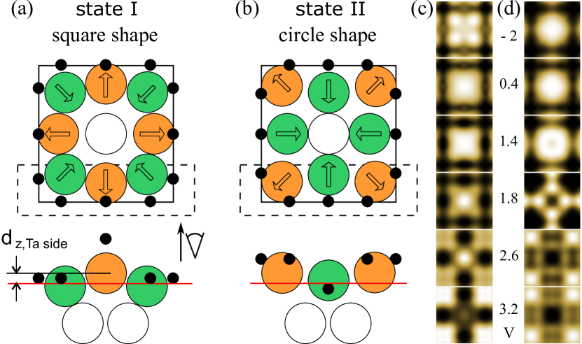
There exists a second energetic minimum for the considered superstructure, which we uncovered accidentally. To obtain this state one should add additional four O atoms around the central Ta atom (see Fig. 1(h) for the notion of the atomic sites), and then relax. Upon removal of these extra atoms and relaxation, the new state, a structural isomer to state I, appears. We denote it as state II (Fig. 2(b)). As we show in Figs. 2(c, d), and will explain later in the text, states I and II correspond exactly to the cross and circular types of 33 plaquettes, which are observed on the STM images. Structural parameters are in agreement with the ones proposed by Titov et al. from LEED and AES experiments.
The revealed zigzag-ordered positions along the O rows are due to a repulsive interaction between the O atoms. In the ideal positions, two adjacent O atoms at the corner have overlap of their Wigner-Seitz spheres, so they act repulsively, especially in state II, where they are elevated. As detailed in the Supplementary Information (Tab. 1), after relaxation, the O atoms at the side positions in state I are higher above the surface by (Fig. 2(a)), and can be viewed as hybridized in a tetrahedral surrounding. Two vacuum-oriented hybrid orbitals host approximately two lone pairs, and are very large in extent (Tab. 2 in the Supplementary Information). The two neighboring O atoms at the corner positions (state I) sidestep into the Ta surface to avoid overlap with O atoms nearby, and form the geometry of the hybridization (Supplementary Information). In the rest of the paper we use the name ‘’ to denote this geometry. In state II, the zigzag-ordered heights are reversed.
To identify the contrast seen in the experimental STM images, we explored the Tersoff-Hamann (TH) model in an analogous way as done by Klijn et al. Klijn et al. (2003) (see also Supplementary Information). In the rest of the paper we show results obtained within the LDA, as the electronic structure remains essentially unchanged by use of GGA and vdW functionals, what we have checked explicitly. All simulated STM images were evaluated at the charge density isosurface value /Å3, corresponding to a tip-to-surface distance of at if the tip is above the center of the 33 plaquette in state I. Independence of the STM contrast on the tip height was checked in experiments and in simulations.
Exploration of the TH approach on both, states I and II, leads to the simulated topographs in Figs. 2(c, d), and the corresponding differential conductances in Figs. 5(k, l) in the Supplementary information. For negative and smaller positive bias up to we observe depressions along the O rows being maximal at the corner positions, and protrusions above the Ta atoms. The latter match perfectly the square (I) and circular (II) shapes seen in STM images around the Fermi energy (Fig. 1(b, c) and Fig. 5 in Supplementary Information), and we therefore conclude that, in this bias regime, the depression lines correspond to the O rows.
Oxygen is typically seen in low-bias STM images as depression as discussed in a number of papers Sautet (1997); Diebold et al. (1996); Woolcot et al. (2012); Picone et al. (2010); Sun (2014). Similar to TiO2 Diebold et al. (1996); Woolcot et al. (2012), the - states of the transition metal atom decay much slower into the vacuum above the surface as compared to the O states. This effect overcompensates the stronger exposure of the O atoms to the STM tip expected from their position above the Ta atoms.
For larger positive bias above , both, for states I and II, the simulated STM images show a contrast reversal (Fig. 2(c,d)). The cross-shaped depression relocates to the center and side Ta atoms. This nicely reproduces the contrast reversal observed experimentally around (c.f. Figs. 1(c-e)). As we will see below, it originates from a redistribution of the electronic density, i.e., less density appears in the vacuum above these Ta atoms at the corresponding bias voltage.
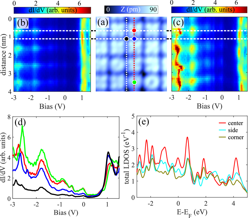
Fig. 3 shows spatially resolved STS data. Figs. 3(b, c) depict 2D colormap representations of STS data acquired along one line on top of the row of O atoms and one line across the Ta plaquettes marked by the white and red dashed lines in Fig. 3(a), respectively. At negative bias the intensity is largest above the Ta plaquettes ((b, c), top horizontal dashed line) and reduced above the O rows (bottom horizontal dashed line). This contrast is reversed at positive sample bias around , where the intensity is shifted towards the O rows and strongest on the corner O atoms (see bottom horizontal dashed line in (b)). This is further evident from the panel (d) where we plot spectra taken at the four characteristic locations marked by the correspondingly colored circles in panel (a). Here, in the negative bias regime, the intensity on the central Ta atoms is larger than that on the side and corner O atoms, while the situation is reversed for positive bias around .
These experimental STS results are compared to the calculated LDOS within empty spheres arranged along the topographic isosurface at a bias of (i.e., above the contrast reversal, see Fig. 9 in Supplementary Information). The calculated LDOS shows a dominating weight above the Ta as compared to the O atoms up to about . A shift of the vacuum LDOS from the Ta to the O atoms above is in qualitative agreement with the STS results.
In the following, we discuss the appearance of the two metastable O superstructures (I and II) and the connected features in more detail. The clean Ta(001) surface represents a sparse structure of atoms, and during annealing, the O atoms diffuse to positions providing the strongest bonds. It was shown for Ta(001) that O atoms do not penetrate into the bulk Drandarov and Kanev (1973). As shown by our calculations within LDA, during chemisorption an individual O atom would prefer the (probably off-central) pyramidal hollow position as it has lowest energy. The adsorption energy at the two-fold bridge position and in the state (elevated above the surface) is higher compared to the hollow position, and even higher in the state. However, experimentally, after the formation of the reconstruction, we see the O atoms in the bridge positions. This discrepancy is resolved by considering a second O atom nearby. The situation is similar to the CO activation, when in the hollow position the bonding orbitals of an O atom are more saturated, so that the bridge position is preferred as it remains chemically more active, and thus it can react with other O atoms Zhang and Hu (2000); Diebold et al. (1996). Indeed, within the calculations we find that two nearby O atoms at bridge positions (along [100] or [010]), both in the state, have the lowest energy, while one O atom at the bridge () and one at the closest hollow position is higher, and both at the hollow positions even higher in energy.
The adsorption energy is smaller in state I than in state II by (LDA) (Tab. 1 in Supplementary Information). Therefore, the comparatively rare experimental appearance of state II can be explained by the necessity of the specific condition to rearrange bonds inside the plaquette. One of the reasons is an obtained instability of two nearby O atoms along the [110] or [10] direction, both in the elevated state: without any supporting orbital mechanism, one of the two drops immediately into the nearest hollow position.
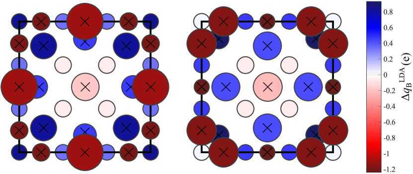
We also provide a charge transfer examination within the surface by means of the BCA Bad (Fig. 4). A pronounced charge polarization emerges as the O atoms try to reach the O-2 state within the and states, which enhances ionicity of all surface atoms. In general, BCA yields larger estimates for the charge transfer than the iterative Hirshfeld algorithm (which we have checked explicitly with vdW functionals), but still showing similar tendencies. Bučko et al. observed an agreement between the iterative Hirshfeld and Born effective charges for ionic crystals Bučko et al. (2014). Thus, the occured reconstruction and buckling of the surface Ta atoms are likely to be a polarization-driven distortion.
The BCA result also implies some important considerations for the electronic properties of the surface. We see a pronounced accumulation of negative charge (Fig. 4) at oxygen locations. As a simple approximation, this can be regarded as a local electrostatic potential (ESP) Kakekhani et al. (2018), additionally acting on the surface near the oxygen rows. Together with filled O states, which are located far below the Fermi level (see Supplementary Information), the ESP will lower the tunneling probability at these sites. Extraordinarily, the central Ta atom is also slightly negatively charged in both structural states. In state II there is less amount of available electronic states at the central Ta atom (Supplementary Information), so it frequently appears as darker spot in STM images. The enhanced ionicity is probably also responsible for the gap opening in the STS curves (Fig. 3(d)).
Large volumes of charge spheres at locations maps very well to the picture of lone pairs of oxygen (see Supplementary Information for more details). These spheres are very close to the central Ta atom and, taken as lone-pairs, are suggested to induce static dipoles at the nearest atoms Sun (2014). Indeed, we see enhanced polarized states on the central Ta atom (Fig. 3(e)). Due to the smearing of the DOS at the tip positions, and the outward and inward curvatures of protrusions and depressions, respectively, the antibonding dipoles can be observed in the STS curves above on all regions of the surface, while below the peaks are mostly due to the lone pairs Sun (2014) (see also Supplementary Information). The interplay between antibonding electronic states of O and corner Ta atoms with polarized - states of the central Ta atom is the source of the observed contrast reversal (Supplementary Information).
The pronounced bonding and antibonding peaks in the central Ta states at approximately , , , and (Fig. 3(e)) can mediate the electrostatic interaction with adsorbates possessing a dipole moment Kakekhani et al. (2018). This means also, that induced dipole excitations would lead to vdW forces acting between the central Ta atom and such polarizable atoms and molecules. In state II, we observe the intensity of polarized peaks being twice lower (Fig. 9 in Supplementary Information).
In summary, we have unravelled the complex atomic structure of the Ta(001)-p(33)-O surface. There is, at least, one extra theoretically uncovered metastable surface superstructure (state II). The way we obtained this state points to the presence of oxygen vacancy defects during formation of the surface. The enhanced oxygen vacancy diffusion was shown to be the source of the adaptive crystalline structure in amorphous and crystalline forms of Ta2O5 Jiang and Stewart (2016), an experimental prototype for the resistive random access memory. Recently Lee et al. (2017), also stable polarons were predicted to exist in charged vacancy sites that should affect the carriers mobility. The system under study is presumably a low-dimensional fellow of the tantalum pentoxide family, sharing a common feature: structural diversity driven by vacancies due to the alternation of bent () and aligned () Ta-O-Ta geometries. We also show that calculated static polarization properties of the surface alters in respect to the type of oxygen row in the metastable state. The surface dipoles induced predominantly in state I will have important implications for the adsorption geometry of transition metal adatoms towards the use as a platform for Majorana physics.
Acknowledgements.
We acknowledge financial support from the Deutsche Forschungsgemeinschaft (DFG) through Project No. SFB668-A3 and A1, and the European Union’s Horizon 2020 research and innovation program under grant agreement No. 696656 - GrapheneCore1. Work of RW and AK was funded by ERC via the Advanced Grant ASTONISH (No. 338802). We thank Carmen Herrmann, Elisaveta Kovbasa, Malte Harland, Frank Lechermann, Vladimir Antropov, Sergey Brener and Tomáš Bučko for helpful discussions.–
Supplementary Information
I Surface preparation
The Ta(001)-p(33)-O surface was prepared by first sputter cleaning of a single crystal of Ta(001) using high energy () Ar+ ions, followed by repeated cycles of annealing at ∘C in presence of O atmosphere (1) and flashing up to ∘C. The sample was then transferred into the STM, which has a base pressure of 5, where it was cooled down to the base temperature of Cornils et al. (2017).
II DFT calculations
DFT was done in the framework of the VASP package with the projector augmented-wave (PAW) basis set Kresse and Furthmüller (1996); Blöchl (1994). To avoid mirror polarizations due to the supercell repetition, the atomic arrangement was chosen mirror symmetric to the central layer within a slab of five 99 Ta layers. In this way the supercell contains 12 O and 45 Ta atoms. The Brillouin zone was covered by a 661 -centred -point mesh, and convergence with respect to the number of -points was tested. All calculations were performed magnetically, and the surface turned out to be non-magnetic everywhere and in all cases considered. For the exchange-correlation energy two different choices were made with the local-density approximation (LDA) and the generalized gradient approximation (GGA) in the variant of Perdew-Burke-Ernzerhof (PBE) Perdew et al. (1996). We included local Coulomb correlation via DFT+ from the outset by choosing and for O atoms, which was found to be relevant for oxidized transition-metal surfaces Nekrasov et al. (2000). Relaxations were performed until forces were below 5. For the calculation of the DOS the number of bands was increased from around 372 (LDA) or 210 (GGA) to around 400 bands, and the energy cutoff from to , to assure an accurate description of the states above the Fermi energy, and which smoothed the simulated STM maps (see Sec. “Differential conductances and topographs” below). These were generated with a Mathematica code available online CSW .
III Differential conductances and topographs
For the simulated STM maps, we applied the Tersoff-Hamann model in an analogous way as done by Klijn et al. Klijn et al. (2003), where at sufficiently low voltages the signal was related to the LDOS of the surface by
| (1) |
Here, the tip DOS is assumed to be constant around and between the Fermi levels of tip and substrate, and is the transmission coefficient, with the decay rate. The surface is covered by the - coordinates, is the perpendicular distance of the tip, and the applied bias voltage between tip and surface. The constant-current topography is obtained by considering the tunneling current
| (2) |
at a fixed value. The quantity on the r.h.s. is identical to the integrated LDOS of the surface at the position of the tip. Plugging the constant-current topography into Eq. (1), one obtains the signal at constant current.
IV Oxygen adsorption and tantalum reconstruction
Tab. 1 contains the relevant parameters of the (33)O superstructure on Ta(001). The termination of the Ta crystal leads to a compression of the outer surface layers: in the LDA, the first interlayer distance differs from the second interlayer distance by only , but from the bulk value by . For the clean Ta surface (not shown), the first to second interlayer distance ratio is , which is already near the ratio between the first interlayer distance and the bulk value of (for comparison, a compression of was reported in Ref. Bartynski et al. (1989); and our GGA calculations yield a first to second interlayer distance ratio of for clean Ta(001) (also not shown)). The O adsorption thus reduces the compression of the Ta surface layers considerably.
The collection of surface atoms has been decomposed into trimers (a collection of three atoms) containing one O and its adjacent two Ta atoms, or one Oside and two Ocorner, or one Taside and two Tacorner. As can be seen from the surface to subsurface interlayer distances , the GGA yields a slightly decompressed surface structure and overall greater bond lengths compared to the LDA. This is a well-known underestimation of the bond-lengths inside L(S)DA Haas et al. (2009). Accordingly, the adsorption energies in the GGA are smaller than in the LDA, but the differences in of the two metastable states are nearly the same for both functionals: in the LDA and in the GGA (likewise for the total energies : in the LDA, in the GGA). As the bonds are generally larger in the GGA, the angles in all trimers of the surface layer are sharper.
The strongest variation is the interchange of the O atom heights between state I and II (i.e. of the Ocorner-Oside-Ocorner trimer, highlighted in blue). While the adsorption height of Oside above the surface is large in state I, in state II Ocorner is elevated (both in gray). Furthermore, the Ocorner-Oside distance is considerably decreased in State II (highlighted in green), leading to a potential overlap of their Wigner-Seitz spheres with radius . The same applies to the distance between two adjacent Ocorner in state I. The distance between the Ocorner in the structure with ideal positions as shown on Figs. 1(g) and (h) of the main manuscript is rather small with . The reconstruction within the Ta surface layer is illustrated by the angles showing substantial deviations from 180∘, the vertex of which point in different directions depending on the state (Fig. 2 of the main manuscript). Furthermore, there appears Ta buckling, as can be seen from the corresponding distances , which is also indicated in Figs. 2(a) and (b) of the main manuscript.
| state I (square-shaped) | state II (circle-shaped) | ||||||
| \stackon/ (eV)functional + | trimer | (Å) | (Å) | (∘) | (Å) | (Å) | (∘) |
| LDA -617.84/7.43 (I) -622.16/7.79 (II) | Taside - Oside - Taside | 1.92 | 1.19 (1.25, 0.06) | 103.73 | 1.96 | -0.11 (-0.09, 0.02) | 186.56 |
| Tacorner - Ocorner - Tacorner | 1.97 | 0.08 (0.03, -0.05) | 171.12 | 1.95 | 0.72 (0.77, 0.05) | 106.41 | |
| Tacorner - Taside - Tacorner | 3.02 | 0.11 (0.06, -0.05) | 162.30 | 3.41 | -0.03 (0.02, 0.05) | 193.39 | |
| Ocorner - Oside - Ocorner | 3.35 | 1.22 (1.25, 0.03) | 137.28 | 2.62 | -0.86 (-0.09, 0.77) | 218.47 | |
| Tacenter - Tasurface | -0.04 | -0.26 | |||||
| Tasurface - Tasubsurface | 1.60 | 1.54 | |||||
| GGA -567.06/6.47 (I) -571.30/6.82 (II) | Taside - Oside - Taside | 1.95 | 1.23 (1.30, 0.07) | 101.61 | 2.00 | -0.15 (-0.13, 0.02) | 188.55 |
| Tacorner - Ocorner - Tacorner | 2.00 | 0.06 (0.00, -0.06) | 170.46 | 1.97 | 0.83 (0.89, 0.06) | 104.37 | |
| Tacorner - Taside - Tacorner | 3.00 | 0.12 (0.06, -0.06) | 160.78 | 3.42 | -0.04 (0.02, 0.06) | 194.73 | |
| Ocorner - Oside - Ocorner | 3.37 | 1.30 (1.30, 0.00) | 134.74 | 2.72 | -1.02 (-0.13, 0.89) | 224.31 | |
| Tacenter - Tasurface | -0.04 | -0.30 | |||||
| Tasurface - Tasubsurface | 1.67 | 1.61 | |||||
V Bader charges
The Bader charge analysis associates charge and atom in a rigid manner, separating the Bader volume by the minima in the charge density around atoms (see Ref. Bad and references therein). Tab. 2, and Fig. 4 of the main manuscript, show a pronounced charge transfer from the Ta surface to the O atoms. O atoms acquire more charge as getting closer to the surface, which is known as high electronegativity of oxygen in chemistry. Accordingly, the O atoms do not reach the complete O-2 state, as well as the Ta surface atoms do not arrive at the complete Ta+ state either. For both states (I and II) Tacorner donate more charge as they are attached to two O atoms. In respect to the functionals, the charge transfer within the system is more pronounced in the LDA than in the GGA, again, due to the increased bonding in the LDA.
More interestingly, while the Bader charge analysis considers the surface region around Tacenter in both states as negatively charged, the Ta region is already nearly charge neutral. To some extent, the subsurface Ta layers can be traced back to the almost neutral, but still slightly negative (below ) clean Ta(001) surface and its subsurface, which itself originates from undercoordination due to termination of the crystal. Within the LDA and in state I, Ta donates a considerable amount of its charge to its four adjacent Ocorner due to the smaller O height in this configuration. In general, we see that the distribution of the charge around Tacenter is very different between state I and state II, that should be of cruicial importance for the adsorption of polarizable atoms and molecules on this surface.
The Bader volumes around each atom were assigned to spheres centered at the atomic sites. The Bader radii show a rather diverse behavior. While the Bader charges are larger in the LDA than in the GGA, the Bader radii are only larger if the O atom is inside the surface. If the O atom is elevated above the surface, the Bader radius becomes smaller in the LDA than in the GGA, although it holds more charge. In contrast to that, for each functional itself Bader charges and radii behave proportionately to each other. The Bader radius is larger for the Ta atoms, of which their adjacent O atom is lying inside the Ta surface. Finally, the Ta surface atoms always have larger Bader radii than the subsurface atoms, because the surface compression is lifted by O adsorption, and surface atoms have access to the vacuum.
In connection with the adsorption of polarizable atoms and molecules, the Bader spheres of Oside and Tacenter are nearer to each other in state I than in state II. That contributes to the differences in the Tacenter DOS between the two states.
| pattern | ion | ||||
|---|---|---|---|---|---|
| State I (square) | Ocorner | 1.21 | 1.14 | 1.74 | 1.66 |
| Oside | 1.12 | 1.05 | 3.58 | 3.69 | |
| Tacorner | +0.80 | +0.70 | 2.57 | 2.49 | |
| Taside | +0.45 | +0.41 | 2.36 | 2.21 | |
| Tacenter | 0.19 | 0.24 | 2.73 | 2.68 | |
| Ta | +0.81 | +0.75 | 1.57 | 1.59 | |
| Ta | +0.32 | +0.37 | 1.57 | 1.58 | |
| Ta | 0.06 | 0.01 | 1.65 | 1.65 | |
| State II (circle) | Ocorner | 1.18 | 1.10 | 2.90 | 2.99 |
| Oside | 1.24 | 1.17 | 1.50 | 1.49 | |
| Tacorner | +0.91 | +0.88 | 2.03 | 1.92 | |
| Taside | +0.41 | +0.34 | 2.78 | 2.75 | |
| Tacenter | 0.24 | 0.26 | 2.86 | 2.73 | |
| Ta | +0.01 | +0.09 | 1.61 | 1.61 | |
| Ta | +0.44 | +0.37 | 1.56 | 1.59 | |
| Ta | 0.06 | 0.03 | 1.68 | 1.69 |
VI Differential conductance images
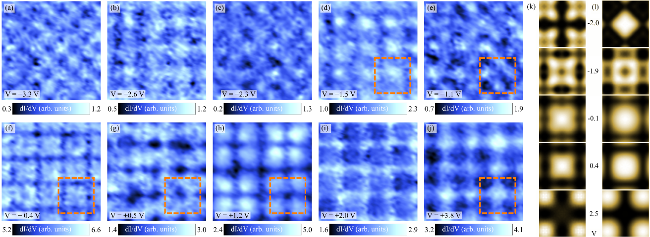
In Fig. 5, we plot experimental images representative for spatial variations of the DOS at a given bias voltage. Here, the area of measurement for the images is the same as in Fig. 1 of the main manuscript. Compared to the STM images, the images show numerous fine variations of the features as a function of bias voltage. In particular, there are at least four contrast reversals similar to the one observed in the STM images, i.e. from 5(d) to (e), from (e) to (f), from (f) to + (g) and from + (i) to + (j). DFT simulation of the conductance leads also to variations of the whole picture, catching contrast reversals in different areas and possible rotation. However, limitations of the TH approach does not allow to discuss it in details. For comparison, we display simulated images of the two states in Fig. 5(k),(l). Similar to the experimental images, they reveal multiple contrast reversals, of which we show a selection. However, a one-to-one correspondence between the different features is hampered by the limitations of the TH model.
VII The Ta2O molecule and orbital hybridization
The Ta-O-Ta trimers mentioned in Sec. “Oxygen adsorption and tantalum reconstruction” comprise (hypothetical) Ta2O molecules. To obtain information on the Ta2O molecule, simplified DFT calculations were performed after singling out the two trimers Taside-Oside-Taside and Tacorner-Ocorner-Tacorner. The DFT setup was left unchanged (see Sec. “DFT calculations”). Relaxation starting from all trimers in state I and II yields two different molecular geometries (Tab. 3), which were found to be stable upon perturbations w.r.t. their positions.
The first and second molecule listed in Tab. 3 approximately correspond to the - and -hybridized configuration, respectively: The bonding angle within the state is comparable to the one of the H2O molecule (104.45∘), while in the state the trimer with the central O has an almost linear geometry as predicted by the Valence Shell Electron Pair Repulsion (VSEPR) approach Gillespie (1972). As on the surface, according to the Bader charge analysis the O atoms do not completely reach the O-2 state. So the orbitals, which do not participate in bonding, host incomplete lone pairs.
As a molecule itself, the -hybridized Ta2O has a net magnetic moment of . Furthermore, it is higher in energy by compared to the -hybridized Ta2O molecule. As on the surface, the Bader radius of the O atom in the state is much larger than in the state.
| trimer | (Å) | (∘) | (, O) | (, Ta) | (Å, O) | (Å, Ta) | (, O) | (, Ta) | (eV) |
|---|---|---|---|---|---|---|---|---|---|
| Ta - O - Ta () | 1.91 | 111.63 | 0.99 | +0.50 | 2.34 | 2.22 | 0.00 | 0.00 | -19.77 |
| Ta - O - Ta () | 1.81 | 179.75 | 1.20 | +0.60 | 1.42 | 2.51 | -0.14 | 1.84 | -16.74 |
VIII Density of states and surface chemistry
Characterization of the LDOS in state I: Fig. 7 contains the orbital-resolved DOS projected onto the sites of the O and corresponding nearest Ta atoms within state I. We identify the O states with energies between / and / of Oside/corner as bonding states (Ref. Sun (2014)), which can be explained by the resonance peaks lying within the same energy range for corresponding peaks in Ta and orbitals.
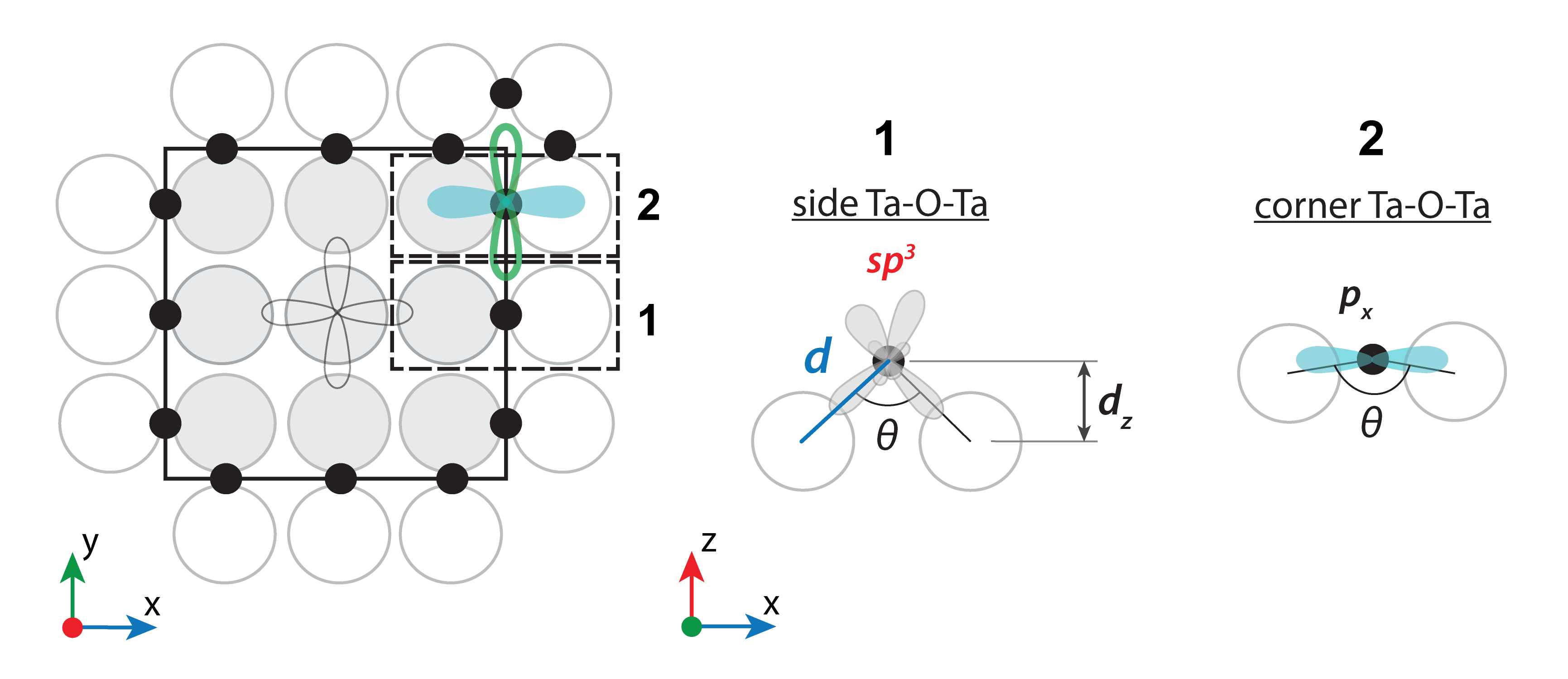
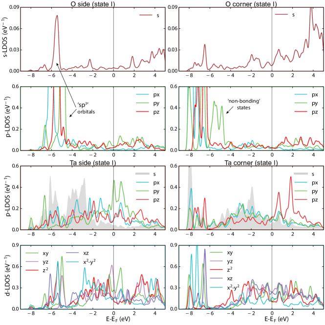
Let us have a closer look on the DOS of Oside and Ocorner which are lying on the vertical O row as shown in Fig. 7. The LDOS of Ocorner shows a set of non-bonding states between and arising from its orbital (Ref. Sun (2014) provides a classification of states seen in LDOS of O adsorbates on transition metal surfaces). This can be understood from geometry: The orbital of Ocorner points to hollows. The orbitals of all O atoms on the vertical O rows are completely filled and contribute only to bonding states with adjacent Ta atoms.
We can apply some quantum chemistry considerations here. According to the Pauling scale of electronegativity, the difference of values between Ta and O in the Ta-O bond reaches 2.0 units, which is close to the border between covalent () and ionic () type of bonding. So we expect a charge transfer towards O in this bond. Based on the surface trimer geometry, we also identify and hybridized O atoms, as in the hypothetical Ta2O molecules. One should note, that for the hybridized O atom embedded into the Ta surface, this localized bonding picture is not relevant, but we use the name, as it carries typical chemical properties. Focusing on Oside in state I, one observes and states located approximately at the same energy that constitutes the hybridization. Then, taking into account the saturation of its hybrid orbitals, two of them are directed towards the adjacent Taside, and the two remaining point towards the vacuum, along the O row and perpendicular to the other two hybrid orbitals. These host the lone pairs (or non-bonding states), and we argue that these states have important implications for all chemical properties of the system. In the DOS one can see that orbitals of and character are higher in energy, in agreement with the local arrangement. We also identify non-bonding states between and up to the Fermi energy, and anti-bonding states above .
Another type of O atom in state I, the -hybridized Ocorner, has a more complex electronic structure. First, the state is characterized by a higher electronegativity of the trimer-central atom than the state, because it has a larger -state contribution (see “Bader charge section” in Tab. 2). Second, there is the already mentioned non-bonding set of states for the orbital. It is possible, that this orbital is rotated towards the orbital of the nearest Oside, being aligned inside the O row. Third, there are clear -bonding and anti-bonding features on spectra of neighboring Ta atoms.
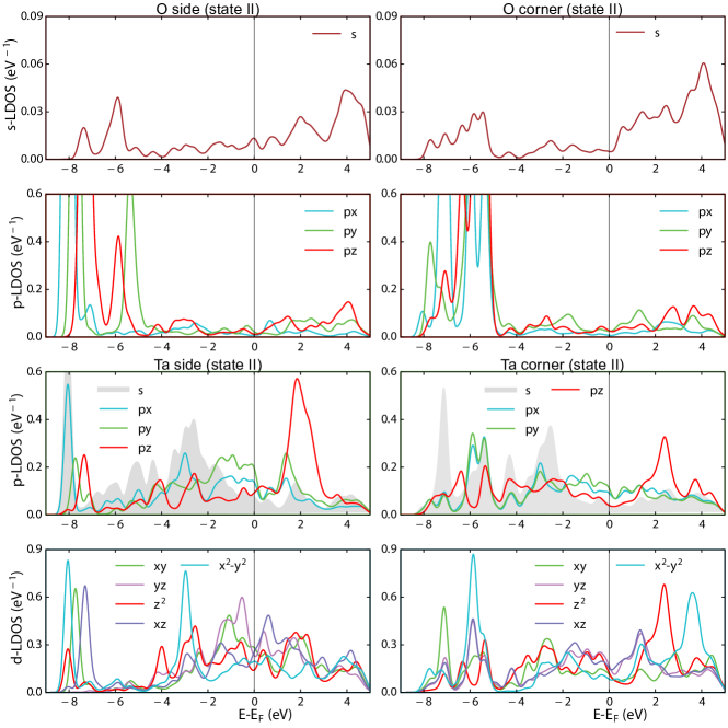
Characterization of the LDOS in state II: The O-LDOS in Fig. 8 show a reversed tendency in their behavior, which corresponds to the reversed adsorption heights within the O rows. We suggest that the Oside and orbitals form a linear combination as , with the one lobe pointing to the close-by orbitals, and the one pointing into the bulk containing the bonding states. Tacorner now shows excitations being more pronounced in the and orbitals as compared to Taside in state I (also due to polarizations induced by lone pairs; to be discussed below), because the two Ocorner are now elevated above the surface, and in the analogous state of Oside within state I. The Taside and Tacorner orbitals in state II show a reversal in excitation weights compared to state I as well.
Effects of and hybridization on adsorption geometry: One can understand the adsorption geometry with the help of the proposed and hybridizations, and the superstructure provided in Tab. 1, which is depicted in Figs. 2(a) and (b) of the main manuscript. As we mentioned, the two bonding orbitals of the hybridized Oside in state I point to the adjacent Taside, with both DFT functionals having a slightly smaller bonding angle than the H2O molecule (104.45∘; Tab. 1). The two remaining lone pairs point diagonally with their orbital lobes to the vacuum along the O row to form the tetrahedral structure.
According to the Bader charge analysis (Sec. “Bader charges” above), the orbital volumes holding the lone pairs are very large, and interact repulsively with Ocorner, which is then embedded into the Ta surface and forms the geometry of the hybridization (the in-plane orbital hybridizes with atoms nearby). The lobe of its non-bonded orbital parallel to the Ta surface occupies the free space along the (vertical) O row and below the lobes of the -hybridized orbitals of Oside pointing to the vacuum. The geometric situation reverses for State II. As there are more -hybridized O atoms than -hybridized ones in State II, it has a lower total energy compared to State I (Tab. 1). This conclusion can also be drawn from Tab. 3, which shows that the Ta2O molecule in -hybridized configuration has lower energy. To sum up, the repulsive character of the formed oxygen lone pairs in the state should play an important role during oxygen adsorption and is responsible for the observed surface pattern with zigzag-ordered O structure perpendicular to the surface. Depending on the temperature and pressure, the O coverage and repulsive interactions are balanced, and crossing O rows are admitted until the optimal 33 superstructure emerges.
Induced polarization effects: In state I, Oside has approximately two lone pairs in -hybridized orbitals with and contributions. Consequently these can induce dipoles in the Taside orbitals of the same symmetry (the anti-bonding peaks of states above ), although more pronounced in , which is parallel to the two hybrid orbitals carrying the suggested lone pairs, and being aligned along the O row. The effect of polarization by induced dipoles is more pronounced on the Ta surface and subsurface atoms (latter not shown) in the central region of the 33 plaquette and below the O row (not shown; for explanations of lone-pair bonding see Ref. Sun (2014)). Excessive peaks above are seen in the Tacenter , , orbitals (Fig. 9), the latter two pointing to Oside and Ocorner. The peaks are due to bonding with the orbital of Tacorner, that is consistent with local geometry. Pronounced and peaks reflect a non-direct hybridization effect that can be cast to the lone-pair idea: these are the lone-pair induced bonding and anti-bonding dipoles. Indeed, the -hybridized states interact with Taside - and -states Walsh et al. (2011), which in turn induce excessive peaks at and states of Tacenter.
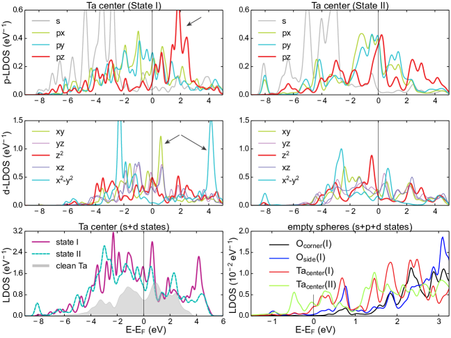
In state II, now the Taside and Tacorner orbitals participate in bonding (Fig. 8). Tacenter, however, does not show any sharp peaks around and above , and has significantly less intensity of the whole spectrum in comparison to state I (Fig. 9). This can be also attributed to the immersed position of the Tacenter in state II. While the long-range effects of the O atoms on the electron structure is less pronounced, the Ta atoms adjacent to the O row show excessive features above and below . Especially in the Tacorner orbital we observe bonding and anti-bonding peaks, which we suggest again to reflect dipoles induced by the presence of two adjacent -hybridized Ocorner atoms.
Explanation of plaquette shapes and contrast reversal: The alternation of the -hybridized O atoms in corner and side positions along the rows leads to the additional broader darkening at its locations on the maps. This effect tunes the square-shaped ( atom at side positions) and circle-shaped ( atom at corner positions) protrusions and goes well in line with the lone-pair concept. Also, in state II, the -orbital weight of Tacenter at low bias is rather small, and thus the central dark spot in low-bias STM images appears. This is because the O atom Bader spheres are farer away (cf. Fig. 4 in the main manuscript) and lone-pair induced anti-bonding dipole production is low.
Backwards, we define the following rules to identify plaquette shapes. All plaquettes have similar features at small bias: deep minima are at the Ocorner, plaquette pattern is present in the system everywhere. We distinguish cross shapes (state I) from circle shapes (state II) by additional minima/maxima:
-
1.
The -state O site (bent geometry) always shows a minimum (less tunneling probability) and it is delocalized (the minimum spot/area appears broad).
-
2.
The -state O site (aligned geometry) also always shows a minimum, but a smaller spot.
-
3.
The Ta regions correspond normally to the protrusions.
Then plaquette attributes goes for the cross shape as:
-
•
Additional broad minima are at Oside sites (),
-
•
maxima are at Tacorner and Tacenter (not strictly).
And for the circle shape as:
-
•
Additional broad minima are at Ocorner sites,
-
•
maxima are at Taside,
-
•
and an additional minimum is at Tacenter (central spot).
The contrast reversal means that there are more states above the corner positions at higher biases. There are four Tacorner in contrast to only one Tacenter. The antibonding states of Ocorner contribute additionally. For the measurement with the STM tip are the Ta and orbitals slightly more relevant, and the charge density from different sites tends to interpenetrate at higher distances above the surfaces, especially as anti-bonding states happen to be more delocalized Jensen et al. (1990). Thus, before the contrast reversal, the STM tip measures the orbitals containing anti-bonding dipole states lowering the work function around Tacenter. At higher bias the anti-bonding states within orbitals of Tacorner contribute more efficiently Sun (2014), also because the potential O-induced gap due to electron-hole production does not prevail anymore.
Summary: In conclusion, we performed a detailed investigation of the experimentally observed electronic properties of the Ta(001)-O surface by means of DFT. Thus, we were able to identify its contrast reversal as seen in the STM images and to predict the adsorption specific properties. One should mention that DFT-GGA in general has a limited access to electrostatic effects on a surface and overall plays towards its metallic character (see, for instance, the experimentally observed induced gap (Fig. 3)). The parental bulk material, especially for the local structure containing the -hybridized trimer, is tantalum pentoxide Ta2O5 Guo and Robertson (2014); Jiang and Stewart (2016). It is an oxide with a high dielectric constant, and with a reported band gap of 1 - . DFT-GW simulations improved the gap values for the crystalline form of Ta2O5, although insufficiently Lee et al. (2014). The contribution of Ta states in the conductance area for intraplanar bonds was suggested to be the reason for the small gap in -Ta2O5 and -Ta2O5 Lee et al. (2014).
Also, we found the picture of the localized molecular bonds helpful, namely the one in terms of hybrid orbitals hosting non-bonding electrons (lone pairs), that served as a complementary view. Unexpectedly, we could explain some properties of the surface with repulsive and long-range character of the lone-pairs interaction that coincide with DFT results.
The Ta protrusions seen on STM images are due to the dominance of the electronic properties over the structural ones. In particular, we propose lone-pair induced anti-bonding dipole states, and anti-bonding -bonded states should play an important role in the physics of the surface. These states above lower the work function, and thus enhance the tunnel current. At higher bias these lead to the contrast reversal.
We see that polarization properties differ in state I and II of the O-reconstructed Ta(001) surface. The arrangement of - and -hybridized O atoms along the rows induces excitations in the center of the 33 plaquette of state I by means of indirect hybridization, but much less in state II. It is Oside in state I, which has the largest Bader radius, and its Bader sphere has the highest proximity to the one of Tacenter. The inhomogeneous electrostatic texture (cf. Fig. 4 of the main manuscript) was found to be marked with an unusual formally negative charge on Tacenter. The pronounced bonding and anti-bonding peaks in the surface Ta states at approximately , , , and can mediate the electrostatic interaction with adsorbates possessing a dipole moment Kakekhani et al. (2018). This also means that the induced dipole excitations would lead to vdW forces acting between Tacenter and such polarizable atoms and molecules.
References
- Nadj-Perge et al. (2014) S. Nadj-Perge, I. K. Drozdov, J. Li, H. Chen, S. Jeon, J. Seo, A. H. MacDonald, B. A. Bernevig, and A. Yazdani, Science 346, 602 (2014).
- Ruby et al. (2015) M. Ruby, F. Pientka, Y. Peng, F. von Oppen, B. W. Heinrich, and K. J. Franke, Phys. Rev. Lett. 115, 197204 (2015).
- Ruby et al. (2017) M. Ruby, B. W. Heinrich, Y. Peng, F. von Oppen, and K. J. Franke, Nano Letters 17, 4473 (2017).
- Jeon et al. (2017) S. Jeon, Y. Xie, J. Li, Z. Wang, B. A. Bernevig, and A. Yazdani, Science 358, 772 (2017).
- Kim et al. (2018) H. Kim, A. Palacio-Morales, T. Posske, L. Rózsa, K. Palotás, L. Szunyogh, M. Thorwart, and R. Wiesendanger, Science Advances 4, eaar5251 (2018).
- Kamlapure et al. (2018) A. Kamlapure, L. Cornils, J. Wiebe, and R. Wiesendanger, Nature Communications 9, 3253 (2018).
- Eelbo et al. (2016) T. Eelbo, V. Zdravkov, and R. Wiesendanger, Surface Science 653, 113 (2016).
- Titov and Jagodzinski (1985) A. V. Titov and H. Jagodzinski, Surface Science 152, 409 (1985).
- Kuznetsov et al. (2010) M. V. Kuznetsov, A. S. Razinkin, and A. L. Ivanovskii, Physics-Uspekhi 53, 995 (2010).
- Razinkin and Kuznetsov (2010) A. S. Razinkin and M. V. Kuznetsov, The Physics of Metals and Metallography 110, 531 (2010).
- Heinrich et al. (2004) A. J. Heinrich, J. A. Gupta, C. P. Lutz, and D. M. Eigler, Science 306, 466 (2004).
- Hirjibehedin et al. (2007) C. F. Hirjibehedin, C.-Y. Lin, A. F. Otte, M. Ternes, C. P. Lutz, B. A. Jones, and A. J. Heinrich, Science 317, 1199 (2007).
- Cornils et al. (2017) L. Cornils, A. Kamlapure, L. Zhou, S. Pradhan, A. A. Khajetoorians, J. Fransson, J. Wiebe, and R. Wiesendanger, Phys. Rev. Lett. 119, 197002 (2017).
- Guo et al. (2017) Y. Guo, M. Bo, Y. Wang, Y. Liu, C. Q. Sun, and Y. Huang, Applied Surface Science 396, 177 (2017).
- Bo et al. (2018) M. Bo, L. Li, Y. Guo, C. Yao, C. Peng, and C. Q. Sun, Applied Surface Science 427, 1182 (2018).
- Sun (2014) C. Q. Sun, Relaxation of the chemical bond: skin chemisorption size matter ZTP mechanics H2O myths, Springer Series in Chemical Physics (Springer, Singapore, 2014).
- Koller et al. (2001) R. Koller, W. Bergermayer, G. Kresse, E. Hebenstreit, C. Konvicka, M. Schmid, R. Podloucky, and P. Varga, Surface Science 480, 11 (2001).
- Brambilla et al. (2013) A. Brambilla, A. Calloni, A. Picone, M. Finazzi, L. Duò, and F. Ciccacci, Applied Surface Science 267, 141 (2013).
- Zhang and Hu (2000) C. J. Zhang and P. Hu, Journal of the American Chemical Society 122, 2134 (2000).
- Kresse and Furthmüller (1996) G. Kresse and J. Furthmüller, Phys. Rev. B 54, 11169 (1996).
- Nekrasov et al. (2000) I. A. Nekrasov, M. A. Korotin, and V. I. Anisimov, eprint arXiv:cond-mat/0009107 (2000).
- (22) http://vaspnotes.blogspot.de/2013/09/simulated-stm.html.
- Klijn et al. (2003) J. Klijn, L. Sacharow, C. Meyer, S. Blügel, M. Morgenstern, and R. Wiesendanger, Phys. Rev. B 68, 205327 (2003).
- Sautet (1997) P. Sautet, Surface Science 374, 406 (1997).
- Diebold et al. (1996) U. Diebold, J. F. Anderson, K.-O. Ng, and D. Vanderbilt, Phys. Rev. Lett. 77, 1322 (1996).
- Woolcot et al. (2012) T. Woolcot, G. Teobaldi, C. L. Pang, N. S. Beglitis, A. J. Fisher, W. A. Hofer, and G. Thornton, Phys. Rev. Lett. 109, 156105 (2012).
- Picone et al. (2010) A. Picone, G. Fratesi, A. Brambilla, P. Sessi, F. Donati, S. Achilli, L. Maini, M. I. Trioni, C. S. Casari, M. Passoni, A. Li Bassi, M. Finazzi, L. Duò, and F. Ciccacci, Phys. Rev. B 81, 115450 (2010).
- Drandarov and Kanev (1973) N. Drandarov and V. Kanev, Vacuum 23, 463 (1973).
- (29) http://theory.cm.utexas.edu/henkelman/code/bader/.
- Bučko et al. (2014) T. Bučko, S. Lebègue, J. G. Ángyán, and J. Hafner, The Journal of Chemical Physics 141, 034114 (2014).
- Kakekhani et al. (2018) A. Kakekhani, L. T. Roling, A. Kulkarni, A. A. Latimer, H. Abroshan, J. Schumann, H. AlJama, S. Siahrostami, S. Ismail-Beigi, F. Abild-Pedersen, and J. K. Nørskov, Inorganic Chemistry 57, 7222 (2018).
- Jiang and Stewart (2016) H. Jiang and D. A. Stewart, Journal of Applied Physics 119 (2016).
- Lee et al. (2017) J. Lee, W. D. Lu, and E. Kioupakis, Nanoscale 9, 1120 (2017).
- Blöchl (1994) P. E. Blöchl, Phys. Rev. B 50, 17953 (1994).
- Perdew et al. (1996) J. P. Perdew, K. Burke, and M. Ernzerhof, Phys. Rev. Lett. 77, 3865 (1996).
- Bartynski et al. (1989) R. A. Bartynski, D. Heskett, K. Garrison, G. Watson, D. M. Zehner, W. N. Mei, S. Y. Tong, and X. Pan, Journal of Vacuum Science & Technology A 7, 1931 (1989).
- Haas et al. (2009) P. Haas, F. Tran, and P. Blaha, Phys. Rev. B 79, 085104 (2009).
- Gillespie (1972) R. Gillespie, Molecular Geometry (Van Nostrand Reinhold Co.,, 1972).
- Walsh et al. (2011) A. Walsh, D. J. Payne, R. G. Egdell, and G. W. Watson, Chem. Soc. Rev. 40, 4455 (2011).
- Jensen et al. (1990) F. Jensen, F. Besenbacher, E. Laegsgaard, and I. Stensgaard, Phys. Rev. B 42, 9206 (1990).
- Guo and Robertson (2014) Y. Guo and J. Robertson, Applied Physics Letters 104 (2014).
- Lee et al. (2014) J. Lee, W. Lu, and E. Kioupakis, Applied Physics Letters 105 (2014).