Hybridization of topological surface states with a flat band
Abstract
We address the problem of hybridization between topological surface states and a non-topological flat bulk band. Our model, being a mixture of three-dimensional Bernevig-Hughes-Zhang and two-dimensional pseudospin-1 Hamiltonian, allows explicit treatment of the topological surface state evolution by continuously changing the hybridization between the inverted bands and an additional ”parasitic” flat band in the bulk. We show that the hybridization with a flat band lying below the edge of conduction band converts the initial Dirac-like surface states into a branch below and one above the flat band. Our results univocally demonstrate that the upper branch of the topological surface states is formed by Dyakonov-Khaetskii surface states known for HgTe since the 1980s. Additionally we explore an evolution of the surface states and the arising of Fermi arcs in Dirac semimetals when the flat band crosses the conduction band.
pacs:
73.21.Fg, 73.43.Lp, 73.61.Ey, 75.30.Ds, 75.70.Tj, 76.60.-kI Introduction
The research on topological materials constitutes one of the most active areas in modern condensed matter physics. Initiated by Kane and Mele, who introduced topology as a new property of two-dimensional (2D) insulators Kane and Mele (2005), their idea has subsequently been generalized to three-dimensional (3D) materials Fu et al. (2007), yielding a whole family of novel topological insulators (TIs). In general, the nontrivial topology of TIs arises from the inversion between two bands with opposite parity, resulting in the appearance of gapless states at the boundaries, which are insensitive to impurities and disorder Moore and Balents (2007); Roy (2009); Hasan and Kane (2010); Qi and Zhang (2011). In 2D TIs counter-propagating one-dimensional (1D) gapless states with opposite spin arise at the edges while 3D TIs feature helical surface states consisting of a single Dirac cone, where the spin points perpendicular to the momentum.
To date multiple 2D and 3D TIs have been experimentally verified (2D TIs Bernevig et al. (2006); König et al. (2007); Liu et al. (2008); Krishtopenko and Teppe (2018a); Krishtopenko et al. (2018); Wu et al. (2018); Krishtopenko and Teppe (2018b); 3D TIs Xia et al. (2009); Zhang et al. (2009); Chen et al. (2009); Hsieh et al. (2009); Fu (2011); Hsieh et al. (2012); Dziawa et al. (2012); Okada et al. (2013)), yet many materials with inverted band structure are bulk metals with additional helical surface states. The most prominent example for this case is the HgTe-class. Here the presence of the heavy-hole band in combination with an inverted pair of the electron and light-hole bands transform HgTe into a bulk semimetal. In order to observe the topologically nontrivial surface states, as predicted by the theoretical analysis based on the topological invariant Fu and Kane (2007), it is necessary to open a gap between conduction and valence band. In the 3D case this can be achieved by applying tensile biaxial strain to the HgTe bulk film Fu and Kane (2007); Dai et al. (2008) which has been demonstrated experimentally in Ref. Brüne et al. (2011).
Theoretically the appearance of surface states in 2D and 3D TIs can be understood within the Bernevig-Hughes-Zhang (BHZ) model describing the band inversion in 2D Bernevig et al. (2006) and 3D systems Zhang et al. (2009). However, in addition to the Dirac-like surface states arising from the band inversion, gapless HgTe should also host parabolic Dyakonov-Khaetskii (DK) surface states, theoretically predicted in the 1980s Dyakonov and Khaetskii (1981). As the DK states are caused by the coupling between the light-hole and heavy-hole band, they should remain even in the presence of the strain-induced band gap Kibis et al. (2019). Thus, the complete picture of the surface states in strained HgTe should differ significantly from the predictions based on the 3D BHZ model Zhang et al. (2009). The picture of the surface states becomes even more complex in the case of compressive biaxial strain, when the and bands touch at certain points of the Brillouin zone Mahler et al. (2019), which is particularly similar to unstrained Cd3As2 crystals Bodnar ; Akrap et al. (2016); Desrat et al. (2018) known to be 3D Dirac semimetals.
In order to gain better insight into this particular query we investigate analytically the transformation of Dirac-like surface states induced by the hybridization between the inverted and bands with an additional heavy-hole band. To include an additional band, we have combined the 3D BHZ Hamiltonian Zhang et al. (2009) with the 2D pseudospin-1 Dirac-Weyl Hamiltonian (cf. Refs Malcolm and Nicol (2015); Raoux et al. (2014)) by introducing an effective hybridization strength. This allows us to explore the evolution of topological surface states at different position of the ”parasitic” band by varying the hybridization strength. At a specific value of hybridization strength, our linear model qualitatively represents the picture of the surface states in the vicinity of the point known from the tight-binding calculations for Cd3As2 Wang et al. (2013) and HgTe Chu et al. (2011). The results demonstrate that the parabolic Dyakonov-Khaetskii surface states known from HgTe Dyakonov and Khaetskii (1981) stem from the modification of the Dirac-like surface states by a hybridization with an additional band in the bulk.
The paper is structured as follows. We introduce a general analytical model based on a combination of the 3D BHZ and 2D pseudospin-1 Dirac-Weyl Hamiltonian in Section II. Subsequently we discuss the topological surface states at different strengths of the hybridization with the flat band as well as for different boundaries at different position of the flat band, including the 3D TI and Dirac semimetal cases. Finally, the main results are summarized in Section IV.
II Theoretical model
For the analytical model we first consider a ”modified” 6-band Hamiltonian including a variable hybridization with a ”parasitic” bulk band:
| (1) |
Here the asterisk stands for complex conjugation and ”” corresponds to Hermitian conjugation. The elements and in Eq. (1) are written as
| (2) |
and
| (3) |
where with , , being momentum operators. We note that corresponds to a set of zero energies, describes the position of the ”parasitic” band and as well as are the values of velocity for the massless particles. In our case, the , and axes are oriented along the (100), (010) and (001) crystallographic directions. For simplicity, we further assume , which can be found in HgCdTe crystals Orlita et al. (2014); Teppe et al. (2016). The mass parameter describes the inversion of bands with opposite parities at which correspond to the normal band ordering and to an inverted one Bernevig et al. (2006); Zhang et al. (2009).
An important quantity of is the parameter , which describes the hybridization of the topological surface states with the ”parasitic” bulk flat band. An exact value for a given system can by obtained by kp perturbation theory up to linear-in- order developed in the vicinity of critical points of the Brillouin zone considering all point group symmetries of the bulk crystal. For instance, the Hamiltonian in Eq. (1) at is essentially the 6-band Kane Hamiltonian regarding the and bands, which describes the band structure in the vicinity of the point of zinc-blende crystals (see Appendix). This means that, depending on , the Hamiltonian in Eq. (1) interpolates between 3D BHZ Hamiltonian with decoupled flat band at for Bi2Se3-class materials Zhang et al. (2009) and the Kane Hamiltonian at .
Additionally, one can see that in Eq. (1) with , and corresponds, up to a simple unitary transformation, to the 2D pseudospin-1 Dirac-Weyl Hamiltonian for massless fermions (cf. Refs Malcolm and Nicol (2015); Raoux et al. (2014)). We note that , and are all related by unitary transformation. Also there are no quadratic terms considered in and for Eqs. (2) and (3) as their form strongly depends on the crystalline symmetry and may differ for two crystals with different values of . Therefore, the universality of the model cannot be preserved beyond the linear approximation but it is in good agreement with magnetooptical experiments for real crystals with Assaf et al. (2016); Krizman et al. (2018) and Orlita et al. (2014); Teppe et al. (2016); Akrap et al. (2016); Desrat et al. (2018).
Supplementary one can see that in Eq. (1) is invariant under inversion symmetry, but a real crystal may not necessarily feature an inversion center in the unit cell, which can results in additional terms in the Hamiltonian. An explicit form of these terms also depends on the crystalline symmetry and may differ for two crystals with the same value of . For instance, breaking the inversion symmetry in compressively strained HgTe and unstrained Cd3As2, both represented by , results in a transition from Dirac- into Weyl-semimetal in HgTe Ruan et al. (2016) while for Cd3As2 it retains a fourfold degenerate Dirac node Wang et al. (2013). In both crystals, the strength of these terms extracted from experimental data is small Orlita et al. (2014); Teppe et al. (2016); Akrap et al. (2016); Desrat et al. (2018), and can be neglected. Having said that, we will retain the Hamiltonian in a general form for the reasons of universality and explicitly consider the inversion symmetrical case.
Under these assumptions the Hamiltonian in Eq. (1) has three eigenvalues, each double degenerate due to the time-reversal symmetry. The eigenvalues follow the equation:
| (4) |
where , , are the quantum numbers of the momentum operators, , and .
III Topological surface states
For the dispersion of the topological surface states, we further consider an interface between two semiconductors with conventional (, CdTe) and inverted (, HgTe) band structure. Since the position of all the bands can be different on both sides of the interface it is justified to make the parameters and , in addition to , dependent on the coordinates. For coordinates far away from the interface the values of these parameters naturally tend to the values inherent to the bulk materials. However, the concrete form of , and depends on the smoothness of the junction and the crystallographic orientation.
We will consider two different cases, corresponding to the abrupt junction oriented along different crystallographic directions. As for the other parameters, we consider and to be independent of coordinates with the same values from both side of the junction, like it is sufficient for the boundary between CdTe and HgTe Teppe et al. (2016). Under these assumptions it can be seen from Eq. (1), that the Hamiltonian remains Hermitian even in the presence of the junction, presuming the operators , and do not commute.
The initial Schrödinger equation with the Hamiltonian can be considered as a set of differential equations for the envelope functions, resulting in an 66 differential matrix. First, we note that each pair of , and represents the electron states with opposite spin orientation in the given band. Namely, for in HgTe-class materials, they correspond to the , and band, respectively (see Appendix). Second, the absence of k-dependent terms in the diagonal elements allows one to express four of the six envelope functions by the two other functions for the same band. Such procedure, which is known as Gaussian elimination, is often used for multi-band Hamiltonians Pfeffer and Zawadzki (2003); Bernardes et al. (2007); Gavrilenko et al. (2011); Krishtopenko et al. .
Considering the pair of envelope functions we can express the four functions , , , in terms of and by keeping the right order of non-commuting operators. Then, substituting the expressions for , , , into the other two equations, we obtain the energy-dependent Hamiltonian , which describes the evolution of the vector for two spin states:
| (5) |
where is the eigenvalue, and
| (6) |
| (7) |
| (8) |
Here, we kept the previous notations, and , and are the same as for Eq. (4). This changes in the following where they also become dependent on the coordinates:
We note that the eigenvalue problem in Eq. (5) is very similar to conventional Schrödinger equation with the single-band Hamiltonian including non-diagonal spin-orbit interaction Pfeffer and Zawadzki (2003); Bernardes et al. (2007); Gavrilenko et al. (2011). Moreover, the procedure described above can be also performed for the other pairs and of the envelope functions.
Although the energy-dependent Hamiltonian in Eq. (5) is non-Hermitian, its eigenvalues are real and are the same as those of in Eq. (1). Recent progress achieved over the last two decades proves that a consistent quantum mechanics can be also built on non-Hermitian Hamiltonians with symmetry Bender and Boettcher (1998); Bender et al. (2002, 2007), where and are parity and time-reversal operators, respectively. One can see that in Eq. (5) can be presented in the form:
where is a 22 unity matrix, , and are Pauli matrices, , , , are the real functions of k. The Hamiltonian always has the real eigenvalues guaranteed by symmetry (where and is the complex conjugation operator) Bender and Boettcher (1998); Bender et al. (2002). In general, non-Hermiticity arises from the presence of energy or particle exchanges with its environment Konotop et al. (2016); El-Ganainy et al. (2018). The presence of heterojunction in the crystal induces additional interaction between all the bands from the opposite sides of the boundary, which results in the non-Hermiticity of describing the pair .
III.1 Surface states for the boundary parallel to (001) crystallographic plane
Let us now consider an abrupt semi-infinite boundary parallel to the (001) crystallographic plane, placed at . In this case, , and only depend on :
| (9) |
where is a step-like function defined as at and at . As mentioned above, the region I corresponds to CdTe with , while the region II represents HgTe with . We demonstrate in the following, that the step-like interface allows us to calculate the dispersion of surface states analytically at arbitrary values of . However, the analytical solution can be found at for several smooth interfaces as well Tchoumakov et al. (2017).
The step-like form of , and in Eq. (III.1) does not only preserve translation symmetry along the and directions but also facilitates the reduction of the eigenvalue problem in Eq. (5) to a set of homogeneous differential equations for the regions and . Then the dispersion of the surface states can be found by applying the boundary conditions at , which were obtained after integrating Eq. (5) across the small region in the vicinity of . Based on the above arguments, and are the good quantum numbers and the wave-function of the surface states localized in the vicinity of has the form:
| (10) |
where and are written as:
| (11) |
Here, and . Note that Eq. (11) can be also derived from Eq. (4) by formally substituting . One can show that the following functions should be continuous across the junction:
| (12) |
Applying the boundary conditions to and , the secular equation for the non-trivial solution leads to
| (13) |
Equations (11) and (13) give the energy dispersion relations of the surface states. It is seen that the surface states at exist if and are of different sign, which requires different signs of and . Substitution of Eq. (11) into Eq. (13) results in a biquadratic equation, which can be solved analytically.
For simplicity, we set and analyze the case . The latter for instance corresponds to the Kane fermions in unstrained HgCdTe crystals Orlita et al. (2014); Teppe et al. (2016). In this case, Eq. (4) provides an energy dispersion for the bulk states, which is independent of :
| (14) |
while Eq. (13) for the surface states is reduced to
| (15) |
where
| (16) |
One can see that for , i.e in the absence of hybridization with a flat band, in addition to and , Eqs. (15) and (16) also give . The latter coincides with the results obtained within 3D BHZ model with the open boundary conditions Shan et al. (2010).
The presence of hybridization splits initial Dirac-like surface states into several branches below and above the flat bands in the materials at both sides of the boundary. Particularly, the surface states lying between the flat bands and are pushed away from the edges of the flat bands at . At large values of , their asymptotic energies are written as
| (17) |
which can be found from Eqs (15) and (16) with . We note that is independent of only in the linear approximation of in Eq. (1), used for the analytical investigation of the surface states at different values of . Including the quadratic terms, whose explicit form depend on , results in non-zero curvature for . The latter has been shown by numerical tight-binding calculations on cubic lattices for the case of , corresponding to real HgTe crystals Chu et al. (2011).
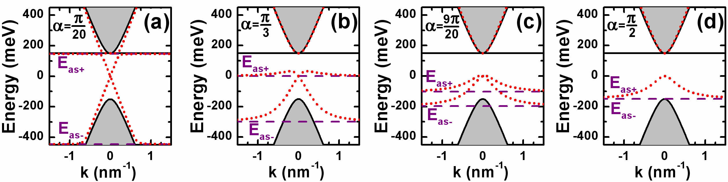
Figure 1 shows the dispersion of the bulk and surface states for different values of in the range for an unstrained film with parameters of HgTe ( meVnm Teppe et al. (2016) and meV) sandwiched between CdTe barriers ( meV). We note that the energy range corresponds to the band gap in the barriers. Although the bulk dispersion in the film remains the same for any values of (due to , see Eq. (14)), the dispersion of the surface states strongly depends on hybridization with the flat bands in both materials. At small values of (see Fig. 1(a)), it consists of four branches , and anticrossing in the vicinity of the crossing points. In this case, the values of and are very close to and , respectively, since in Eq. (17). This picture can be also treated within the conventional degenerate perturbation approach.
With increasing of , the surface states for are pushed away from the energies of the flat bulk bands in the materials at both sides of the boundary toward the regions where these bulk states are absent. This is clearly represented by the evolution of the asymptotic energies and , which are getting closer to each other when increases as shown in Fig. 1(a-c). Note that dispersion of the surface states remains linear in the vicinity of the point of the Brillouin zone. At the specific value of , the asymptotic energies coincide both being equal to , and the surface states become degenerate, see Fig. 1(d). The latter means the absence of odd-in- terms in their dispersion. We note that the surface states, similar to those provided in Fig. 1(b) for , were also obtained by more sophisticated numerical calculations based on tight-binding extension of the 6-band Kane Hamiltonian with square terms Chu et al. (2011). Although, the results of Ref. Chu et al. (2011) depend on the constant of artificial cubic lattice used in the calculations, they qualitatively reproduce the dispersion of the surface states at small quasimomentum obtained from our analytical model at .
In addition to the modification of the surface states in the range of , the hybridization with the flat bulk bands also yields new ”massive” branches in the regions above and below the flat bands. We refer to the upper ”massive” surface states above the flat band as the Dyakonov-Khaetskii (DK) branch. Dyakonov and Khaetskii Dyakonov and Khaetskii (1981) were the first, who predicted the massive states at the surface of HgTe crystal. They derived analytically this branch in 1981 by using Luttinger Hamiltonian for the bands Luttinger (1956) with an open boundary conditions. In 1985, existence of the localized states at the HgTe/CdTe interface was also predicted for the quantum wells Lin-Liu and Sham (1985) and superlattices Chang et al. (1985).
Although the Luttinger Hamiltonian, used in Refs Dyakonov and Khaetskii (1981); Lin-Liu and Sham (1985), does not formally consider the inverted band, this Hamiltonian can be obtained from the 6-band Kane Hamiltonian with the HgTe/CdTe interface by assuming and . Therefore, the upper ”massive” surface states in Fig. 1 and solution of Dyakonov and Khaetskii Dyakonov and Khaetskii (1981), obtained for particular case of , have the same origin. As seen from Fig. 1, such DK branch is caused by the band inversion in the presence of hybridization with the flat bulk band.
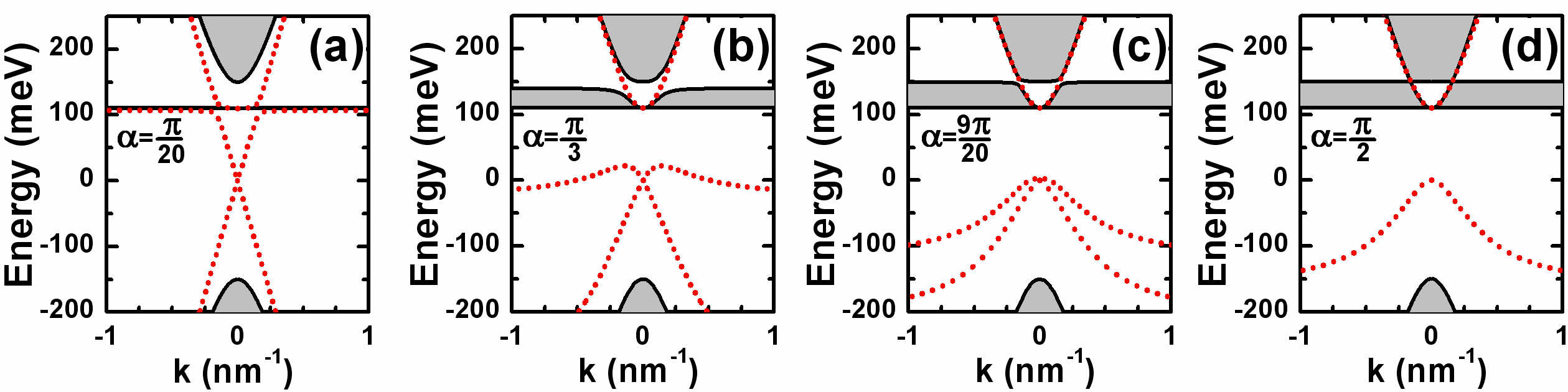
Now we consider a bulk crystal, in which the flat band does not coincide with the bottom of the conduction band, i.e. . The case of corresponds to an external tensile biaxial strain, which opens a band gap, yielding 3D TI state Fu and Kane (2007); Brüne et al. (2011). The opposite case of is realized in the compressively strained HgTe films Mahler et al. (2019) or in unstrained Cd3As2 crystals Akrap et al. (2016); Desrat et al. (2018). As in previous case, we set and assume in CdTe layer.
Fig. 2 shows a picture of the bulk and surface states at different values of in the range for tensile strained film the with parameters of HgTe ( meV) sandwiched between CdTe barriers. Note that now the energy dispersions are calculated numerically on the basis of Eq. (4) and Eqs. (11), (13) for the bulk and surface states, respectively. It is seen that energy of the bulk states and the value of a band-gap between the flat and conduction bands strongly depend on . The maximum gap is achieved in the absence of hybridization, while increasing of leads to a band-gap vanishing. The value of corresponds to a semimetal with circular nodal line at and , where .
As seen from Fig. 2, the surface states in a tensile strained film at different values remain qualitatively the same, as in Fig. 1 for the unstrained film. The main difference is seen in the DK branch, which now exists in the band-gap for the bulk states for all . This is consistent with the general topological arguments claiming that tensile strained HgTe is a 3D TI with gapless surface states Fu and Kane (2007). However, these surface states can not be represented by massless Dirac fermions, as it is stated in some experimental works on HgTe strained by a CdTe substrate (see, for instance, Refs. Kozlov et al. (2016); Thomas et al. (2017); Noel et al. (2018)). Fig. 2 clearly shows that the surface states at the HgTe/CdTe boundary of strained HgTe-based 3D TI are ”massive” due to the hybridization with heavy-hole band and represented by DK branch Dyakonov and Khaetskii (1981).
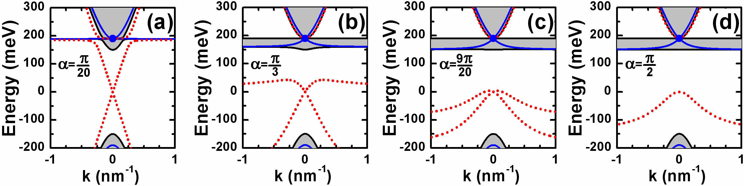
In the opposite case of , the flat band crosses the conduction band at certain points of the Brillouin zone at yielding a 3D Dirac semimetal. At these points, the conduction and flat valence bands can be considered as two highly anisotropic and tilted cones Wang et al. (2013); Akrap et al. (2016); Desrat et al. (2018), whose nodes lie at and with , see Eq. (4). Note that at , the crossing points are located at the sphere defined by , and the 3D Dirac semimetal state does not arise.
Fig. 3 presents the bulk and surface states in a film with (where meV) at different strengths of hybridization with a flat band. As in the previous case of , the bulk and surface states both depend on the values of . Interestingly, the dispersion of the surface states in Fig. 3 for all starts from projection of the bulk Dirac nodes. The bulk band dispersion as a function of at is represented by the blue curves. We note that the particular case is in a good qualitative agreement with the picture of the surface states obtained from the tight-binding calculations for Cd3As2 on a tetragonal lattice Wang et al. (2013) (see Fig. 3(a,b) therein).
III.2 Surface states for the boundary parallel to (010) plane
One of the inherent characteristics of the surface states in Dirac semimetals is the existence of a pair of surface Fermi arcs connecting bulk Dirac nodes projected on the surface boundary. The arcs meet at a sharp corner or ”kink” at the projected nodes. Such a kink is not allowed in a purely 2D metal, it is a special feature of the crystal symmetry-protected Weyl structure of the Dirac semimetals Potter et al. (2014). As the Dirac nodes are located along the (001) crystallographic direction, the surface boundary parallel to the (001) plane has no Fermi arcs.
Let us now briefly consider the surface states for the boundary containing two projections of the bulk Dirac nodes at . For the boundary plane parallel to the x-z plane and placed at , , and have a step-like dependence on :
| (18) |
Basing on the arguments similar to the case of (001) interface, the wave-function of the surface states for the (010) boundary has the form:
| (19) |
where and are written as:
| (20) |
where the index corresponds to and , respectively.
Integration of Eq. (5) across the small region of gives the continuity function across the junction:
| (21) |
where and are function of and :
| (22) |
Applying these boundary conditions to and , the secular equation for the non-trivial solution leads to
| (23) |
Substitution of and into Eq. (13) also results in a quadratic equation for and , which can be solved analytically. Such a quadratic equation gives the energy dispersion and energy contours of the surface states for the boundary parallel to the (010) crystallographic plane.
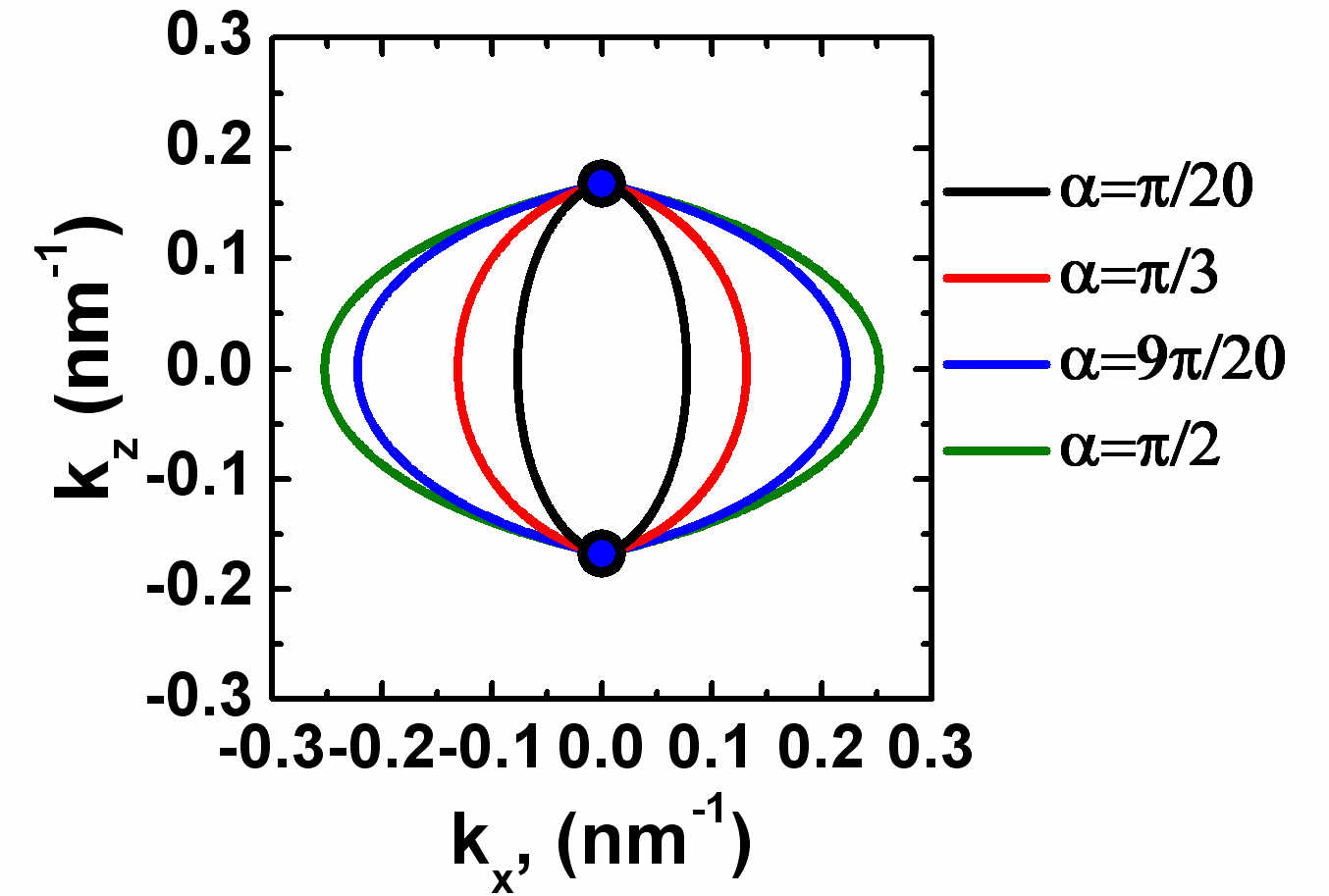
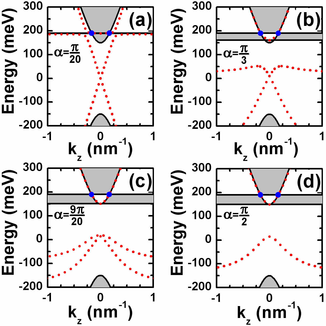
Fig. 4 shows the dispersions of the bulk and surface states as a function of for the bulk film with and (010) surface boundary. Here, we set , , meV and assume . As for the (001) boundary, the picture of surface states for all values consists of two branches above and below the bottom of the conduction band at . As it is seen, the upper DK branch for all crosses the bulk dispersion precisely at the Dirac nodes. This stems from the fact that two separated Dirac nodes are connected by the topological surface states Potter et al. (2014). A current picture of the surface states for is also consistent with the tight-binding calculations for Cd3As2 Wang et al. (2013).
Fig. 5 provides energy contours for the surface states at at different strengths of hybridization with the flat band. In contrast to the (001) boundary, for which the energy contour of the surface states at the Dirac nodes reduces to a point, the nontrivial surface states at the (010) boundary are clearly visible. Its Fermi surface at is composed of two Fermi arcs with the kinks at the projected bulk Dirac nodes. As seen from Fig. 5, the length of Fermi arcs depends on the values of . This means that the period of quantum oscillations originated from cyclotron orbits weaving together Fermi arcs and chiral bulk states Potter et al. (2014), should also depend on the hybridization strength.
IV Summary
In conclusion, we have performed an analytical study of the hybridization between topological surface states and the non-topological flat band in the bulk. It was shown that the hybridization with the flat band divides the initially Dirac-like surface states, derived from the 3D BHZ model, into two branches, one below the flat band and another one above the edge of conduction band. The upper branch at is formed by Dyakonov-Khaetskii surface states Dyakonov and Khaetskii (1981) known for HgTe since the 1980s. Adjusting the hybridization strength, we have explored the evolution of topological surface states in 3D TIs and 3D Dirac semimetals arising at different positions of the flat band. Our results show that the surface states lying inside the band gap of 3D TIs, as well as the Fermi arcs of 3D Dirac semimetals in HgTe and Cd3As2 are represented by the DK branch of the surface states. Although, we have applied the linear approximation for the bulk Hamiltonian, our model qualitatively represents the picture of surface states at small values of k, known for from numerical tight-binding calculations on tetragonal Wang et al. (2013) and cubic lattices Chu et al. (2011). This work paves the way for further analytical investigations of different characteristics of the surface states hybridized with non-topological bands.
Acknowledgements.
The authors gratefully thank S. Gebert (Institut d’Electronique et des Systemes, Montpellier) for the helpful discussions and critical comments. This work was supported by MIPS department of Montpellier University through the ”Occitanie Terahertz Platform”, by the CNRS through LIA ”TeraMIR” and the French Agence Nationale pour la Recherche (Dirac3D project).Appendix: 6-band Kane Hamiltonian
In order to demonstrate that the Hamiltonian in Eq. (1) for corresponds to the 6-band Kane Hamiltonian, we consider the 8-band Kane Hamiltonian Bodnar , whose form is dependent on the choice of the basis set of the Bloch amplitudes for the , and bands. In the given basis set
the 8-band Kane Hamiltonian in the presence of only the linear terms takes the form
| (24) |
Here, is the Kane momentum matrix element, is the spin orbit energy and as well as are the conduction and valence band edges, respectively. We note that the values of , and differ if there is biaxial strain in the (001) crystallographic plane Krishtopenko et al. (2016).
In the limit of large , the Hamiltonian can be easily projected on the subspace, orthogonal to the the split-off band. As we are not interested in terms quadratic in ,the projection is done by simply eliminating the fourth and the eight row and column of the matrix in Eq. (24):
| (25) |
References
- Kane and Mele (2005) C. L. Kane and E. J. Mele, Phys. Rev. Lett. 95, 226801 (2005).
- Fu et al. (2007) L. Fu, C. L. Kane, and E. J. Mele, Phys. Rev. Lett. 98, 106803 (2007).
- Moore and Balents (2007) J. E. Moore and L. Balents, Phys. Rev. B 75, 121306 (2007).
- Roy (2009) R. Roy, Phys. Rev. B 79, 195322 (2009).
- Hasan and Kane (2010) M. Z. Hasan and C. L. Kane, Rev. Mod. Phys. 82, 3045 (2010).
- Qi and Zhang (2011) X.-L. Qi and S.-C. Zhang, Rev. Mod. Phys. 83, 1057 (2011).
- Bernevig et al. (2006) B. A. Bernevig, T. L. Hughes, and S.-C. Zhang, Science 314, 1757 (2006).
- König et al. (2007) M. König, S. Wiedmann, C. Brüne, A. Roth, H. Buhmann, L. W. Molenkamp, X.-L. Qi, and S.-C. Zhang, Science 318, 766 (2007).
- Liu et al. (2008) C. Liu, T. L. Hughes, X.-L. Qi, K. Wang, and S.-C. Zhang, Phys. Rev. Lett. 100, 236601 (2008).
- Krishtopenko and Teppe (2018a) S. S. Krishtopenko and F. Teppe, Sci. Adv. 4, eaap7529 (2018a).
- Krishtopenko et al. (2018) S. S. Krishtopenko, S. Ruffenach, F. Gonzalez-Posada, G. Boissier, M. Marcinkiewicz, M. A. Fadeev, A. M. Kadykov, V. V. Rumyantsev, S. V. Morozov, V. I. Gavrilenko, C. Consejo, W. Desrat, B. Jouault, W. Knap, E. Tournié, and F. Teppe, Phys. Rev. B 97, 245419 (2018).
- Wu et al. (2018) S. Wu, V. Fatemi, Q. D. Gibson, K. Watanabe, T. Taniguchi, R. J. Cava, and P. Jarillo-Herrero, Science 359, 76 (2018).
- Krishtopenko and Teppe (2018b) S. S. Krishtopenko and F. Teppe, Phys. Rev. B 97, 165408 (2018b).
- Xia et al. (2009) Y. Xia, D. Qian, D. Hsieh, L. Wray, A. Pal, H. Lin, A. Bansil, D. Grauer, Y. S. Hor, R. J. Cava, and M. Z. Hasan, Nature Phys. 5, 398 (2009).
- Zhang et al. (2009) H. Zhang, C.-X. Liu, X.-L. Qi, X. Dai, Z. Fang, and S.-C. Zhang, Nature Phys. 5, 438 (2009).
- Chen et al. (2009) Y. L. Chen, J. G. Analytis, J.-H. Chu, Z. K. Liu, S.-K. Mo, X. L. Qi, H. J. Zhang, D. H. Lu, X. Dai, Z. Fang, S. C. Zhang, I. R. Fisher, Z. Hussain, and Z.-X. Shen, Science 325, 178 (2009).
- Hsieh et al. (2009) D. Hsieh, Y. Xia, L. Wray, D. Qian, A. Pal, J. H. Dil, J. Osterwalder, F. Meier, G. Bihlmayer, C. L. Kane, Y. S. Hor, R. J. Cava, and M. Z. Hasan, Science 323, 919 (2009).
- Fu (2011) L. Fu, Phys. Rev. Lett. 106, 106802 (2011).
- Hsieh et al. (2012) T. H. Hsieh, H. Lin, J. Liu, W. Duan, A. Bansil, and L. Fu, Nat. Commun. 3, 982 (2012).
- Dziawa et al. (2012) P. Dziawa, B. J. Kowalski, K. Dybko, R. Buczko, A. Szczerbakow, M. Szot, E. Lusakowska, T. Balasubramanian, B. M. Wojek, M. H. Berntsen, O. Tjernberg, and T. Story, Nat. Mater. 11, 1023 (2012).
- Okada et al. (2013) Y. Okada, M. Serbyn, H. Lin, D. Walkup, W. Zhou, C. Dhital, M. Neupane, S. Xu, Y. J. Wang, R. Sankar, F. Chou, A. Bansil, M. Z. Hasan, S. D. Wilson, L. Fu, and V. Madhavan, Science 341, 1496 (2013).
- Fu and Kane (2007) L. Fu and C. L. Kane, Phys. Rev. B 76, 045302 (2007).
- Dai et al. (2008) X. Dai, T. L. Hughes, X.-L. Qi, Z. Fang, and S.-C. Zhang, Phys. Rev. B 77, 125319 (2008).
- Brüne et al. (2011) C. Brüne, C. X. Liu, E. G. Novik, E. M. Hankiewicz, H. Buhmann, Y. L. Chen, X. L. Qi, Z. X. Shen, S. C. Zhang, and L. W. Molenkamp, Phys. Rev. Lett. 106, 126803 (2011).
- Dyakonov and Khaetskii (1981) M. I. Dyakonov and A. V. Khaetskii, JETP Lett. 33, 110 (1981).
- Kibis et al. (2019) O. V. Kibis, O. Kyriienko, and I. A. Shelykh, New J. Phys. 21, 043016 (2019).
- Mahler et al. (2019) D. M. Mahler, J.-B. Mayer, P. Leubner, L. Lunczer, D. Di Sante, G. Sangiovanni, R. Thomale, E. M. Hankiewicz, H. Buhmann, C. Gould, and L. W. Molenkamp, Phys. Rev. X 9, 031034 (2019).
- (28) J. Bodnar, Proc. III Conf. Narrow-Gap Semiconductors, Warsaw, edited by J. Rauluszkiewicz, M. Górska, and E. Kaczmarek (Elsevier, 1977) pp. 311, see also arXiv:1709.05845 .
- Akrap et al. (2016) A. Akrap, M. Hakl, S. Tchoumakov, I. Crassee, J. Kuba, M. O. Goerbig, C. C. Homes, O. Caha, J. Novák, F. Teppe, W. Desrat, S. Koohpayeh, L. Wu, N. P. Armitage, A. Nateprov, E. Arushanov, Q. D. Gibson, R. J. Cava, D. van der Marel, B. A. Piot, C. Faugeras, G. Martinez, M. Potemski, and M. Orlita, Phys. Rev. Lett. 117, 136401 (2016).
- Desrat et al. (2018) W. Desrat, S. S. Krishtopenko, B. A. Piot, M. Orlita, C. Consejo, S. Ruffenach, W. Knap, A. Nateprov, E. Arushanov, and F. Teppe, Phys. Rev. B 97, 245203 (2018).
- Malcolm and Nicol (2015) J. D. Malcolm and E. J. Nicol, Phys. Rev. B 92, 035118 (2015).
- Raoux et al. (2014) A. Raoux, M. Morigi, J.-N. Fuchs, F. Piéchon, and G. Montambaux, Phys. Rev. Lett. 112, 026402 (2014).
- Wang et al. (2013) Z. Wang, H. Weng, Q. Wu, X. Dai, and Z. Fang, Phys. Rev. B 88, 125427 (2013).
- Chu et al. (2011) R.-L. Chu, W.-Y. Shan, J. Lu, and S.-Q. Shen, Phys. Rev. B 83, 075110 (2011).
- Orlita et al. (2014) M. Orlita, D. M. Basko, M. S. Zholudev, F. Teppe, W. Knap, V. I. Gavrilenko, N. N. Mikhailov, S. A. Dvoretskii, P. Neugebauer, C. Faugeras, A.-L. Barra, G. Martinez, and M. Potemski, Nature Phys. 10, 233 (2014).
- Teppe et al. (2016) F. Teppe, M. Marcinkiewicz, S. S. Krishtopenko, S. Ruffenach, C. Consejo, A. M. Kadykov, W. Desrat, D. But, W. Knap, J. Ludwig, S. Moon, D. Smirnov, M. Orlita, Z. Jiang, S. V. Morozov, V. Gavrilenko, N. N. Mikhailov, and S. A. Dvoretskii, Nat. Commun. 7, 12576 (2016).
- Assaf et al. (2016) B. Assaf, T. Phuphachong, V. Volobuev, A. Inhofer, G. Bauer, G. Springholz, L. de Vaulchier, and Y. Guldner, Sci. Rep. 6, 20323 (2016).
- Krizman et al. (2018) G. Krizman, B. A. Assaf, T. Phuphachong, G. Bauer, G. Springholz, L. A. de Vaulchier, and Y. Guldner, Phys. Rev. B 98, 245202 (2018).
- Ruan et al. (2016) J. Ruan, S.-K. Jian, H. Yao, H. Zhang, S.-C. Zhang, and D. Xing, Nat. Commun. 7, 11136 (2016).
- Pfeffer and Zawadzki (2003) P. Pfeffer and W. Zawadzki, Phys. Rev. B 68, 035315 (2003).
- Bernardes et al. (2007) E. Bernardes, J. Schliemann, M. Lee, J. C. Egues, and D. Loss, Phys. Rev. Lett. 99, 076603 (2007).
- Gavrilenko et al. (2011) V. I. Gavrilenko, S. S. Krishtopenko, and M. Goiran, Semiconductors 45, 110 (2011).
- (43) S. S. Krishtopenko, V. I. Gavrilenko, and M. Goiran, Solid State Phenomena 190, 554.
- Bender and Boettcher (1998) C. M. Bender and S. Boettcher, Phys. Rev. Lett. 80, 5243 (1998).
- Bender et al. (2002) C. M. Bender, D. C. Brody, and H. F. Jones, Phys. Rev. Lett. 89, 270401 (2002).
- Bender et al. (2007) C. M. Bender, D. C. Brody, H. F. Jones, and B. K. Meister, Phys. Rev. Lett. 98, 040403 (2007).
- Konotop et al. (2016) V. V. Konotop, J. Yang, and D. A. Zezyulin, Rev. Mod. Phys. 88, 035002 (2016).
- El-Ganainy et al. (2018) R. El-Ganainy, K. G. Makris, M. Khajavikhan, Z. H. Musslimani, S. Rotter, and D. N. Christodoulides, Nature Phys. 14, 11 (2018).
- Tchoumakov et al. (2017) S. Tchoumakov, V. Jouffrey, A. Inhofer, E. Bocquillon, B. Plaçais, D. Carpentier, and M. O. Goerbig, Phys. Rev. B 96, 201302 (2017).
- Shan et al. (2010) W.-Y. Shan, H.-Z. Lu, and S.-Q. Shen, New J. Phys. 12, 043048 (2010).
- Luttinger (1956) J. M. Luttinger, Phys. Rev. 102, 1030 (1956).
- Lin-Liu and Sham (1985) Y. R. Lin-Liu and L. J. Sham, Phys. Rev. B 32, 5561 (1985).
- Chang et al. (1985) Y.-C. Chang, J. N. Schulman, G. Bastard, Y. Guldner, and M. Voos, Phys. Rev. B 31, 2557 (1985).
- Kozlov et al. (2016) D. A. Kozlov, D. Bauer, J. Ziegler, R. Fischer, M. L. Savchenko, Z. D. Kvon, N. N. Mikhailov, S. A. Dvoretsky, and D. Weiss, Phys. Rev. Lett. 116, 166802 (2016).
- Thomas et al. (2017) C. Thomas, O. Crauste, B. Haas, P.-H. Jouneau, C. Bäuerle, L. P. Lévy, E. Orignac, D. Carpentier, P. Ballet, and T. Meunier, Phys. Rev. B 96, 245420 (2017).
- Noel et al. (2018) P. Noel, C. Thomas, Y. Fu, L. Vila, B. Haas, P.-H. Jouneau, S. Gambarelli, T. Meunier, P. Ballet, and J. P. Attané, Phys. Rev. Lett. 120, 167201 (2018).
- Potter et al. (2014) A. C. Potter, I. Kimchi, and A. Vishwanath, Nat. Commun. 5, 5161 (2014).
- Krishtopenko et al. (2016) S. S. Krishtopenko, I. Yahniuk, D. B. But, V. I. Gavrilenko, W. Knap, and F. Teppe, Phys. Rev. B 94, 245402 (2016).