On-Chip Integration of Single Solid-State Quantum Emitters with a SiO2 Photonic Platform
Abstract
One important building block for future integrated nanophotonic devices is the scalable on-chip interfacing of single photon emitters and quantum memories with single optical modes. Here we present the deterministic integration of a single solid-state qubit, the nitrogen-vacancy (NV) center, with a photonic platform consisting exclusively of SiO2 grown thermally on a Si substrate. The platform stands out by its ultra-low fluorescence and the ability to produce various passive structures such as high-Q microresonators and mode-size converters. By numerical analysis an optimal structure for the efficient coupling of a dipole emitter to the guided mode could be determined. Experimentally, the integration of a preselected NV emitter was performed with an atomic force microscope and the on-chip excitation of the quantum emitter as well as the coupling of single photons to the guided mode of the integrated structure could be demonstrated. Our approach shows the potential of this platform as a robust nanoscale interface of on-chip photonic structures with solid-state qubits.
I Introduction
Single solid-state quantum emitters such as color centers in diamond are promising potential building blocks for future quantum information processing architectures and integrated nanophotonic devices Aharonovich and Neu (2014). The most prominent representative is the nitrogen-vacancy (NV) color center which exhibits coherent optical transitions and long-lived nuclear and electron spins, making it a promising solid-state qubit Gruber et al. (1997); Togan et al. (2010); Maurer et al. (2012) and single photon source Kurtsiefer et al. (2000), but the ongoing search for new solid-state quantum emitters recently revealed a variety of new emitters, e.g. new optical vacancy-impurity defects in diamond Thiering and Gali (2018); Lühmann et al. (2018) and hexagonal boron nitride Tran et al. (2016).
The most fundamental way of interaction with single emitters is free-space optics, but in order to build scalable quantum architectures, deterministic and efficient on-chip integration of one or more quantum emitters in combination with passive optical structures such as cavities and couplers is required Kimble (2008); Benson (2011). One fundamental requirement is the efficient collection and routing of single photons. The commonly used platform silicon cannot be used in most cases since its opaque up to about and a large part of the interesting solid-state emitters emit at visible wavelengths Therefore, in recent years great efforts have been made to develop new platforms for integration of quantum emitters and to demonstrate the assembly of hybrid nanophotonic systems, for example, based on tapered optical fibers Schröder et al. (2012); Liebermeister et al. (2014); Fujiwara et al. (2016); Patel et al. (2016); Schell et al. (2017), in-situ direct laser written Shi et al. (2016) or electron beam lithographed Schnauber et al. (2018), diamond Faraon et al. (2011); Burek et al. (2017); Bhaskar et al. (2017), other dielectric Gschrey et al. (2013); Zadeh et al. (2016); Gould et al. (2016); Kim et al. (2017); Tonndorf et al. (2017); Mouradian et al. (2015); Davanco et al. (2017) or plasmonic structures Kewes et al. (2016); Siampour et al. (2017, 2018).
Each of these platforms poses its own challenges and depending on the selected emitter and specific application, some are better suited than others. One common problem is unwanted background fluorescence from the passive optical structure, as some emitters need to be pumped strongly with green or even blue light. Another crucial aspect is low absorption in the material to minimize losses and enable the fabrication of high-Q resonators. A very well-suited material platform is silica (SiO2) which is thermally grown on silicon (Si), as it offers a broad transparency window from the UV to mid-IR and therefore low fluorescence and losses. However, the index of refraction of SiO2 is rather low (), so in order to allow for a propagating mode within the SiO2, the underlying silicon must to be removed.
In this work we use a free-standing, monolithic SiO2 photonics platform, where rib-waveguides allow efficient guiding of visible light in thermally grown and undoped SiO2 similar to the system introduced by Chen et al. Chen et al. (2012). So far, we have been able to show that this system has a very low background fluorescence, which is well suited for the integration of single photon emitters, and in addition high-Q micro-resonators can be realized Pyrlik et al. (2019). By the numerical analysis of the waveguide structures we present a design that allows an optimal coupling of the guided mode in the waveguide to an external quantum emitter. We also present a 2D tapered section of the waveguide as a mode-size converter to improve the mode overlap with lensed single-mode fibers. After characterizing the fabricated device, we show the functionalization of this nanophotonic platform with a preselected single NV color center hosted within a nanometer-sized diamond Schell et al. (2011), and by detecting the single-photon emission from the integrated waveguide, we were able to demonstrate the coupling between the guided fundamental mode of the SiO2 waveguide and the single quantum emitter.
The integrated platform presented here has the advantage of the ultra-low intrinsic fluorescence when compared to other material such as Si3N4 or doped optical fibers. Its wide transparency window ( - ) is ideal to integrate other solid-state or condensed-phase emitters, e.g. in a hybrid integrated platform. Finally, fabrication is simple and other passive structures such as high-Q microring resonators Pyrlik et al. (2019) or detectors Ferrari et al. (2018) can be integrated.
II System and methods
II.1 Waveguide design and functionalization
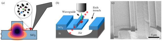
To minimize background fluorescence, the integrated photonic platform was designed to guide the optical mode exclusively within undoped, thermally grown SiO2 which exhibits ultra-low intrinsic fluorescence, even when strongly pumped with a laser Pyrlik et al. (2019). Single NV centers on fabricated devices typically show signal-to-noise ratios of (with subtracted dark count rates). To enable this air-clad waveguide, a supporting membrane is required, resulting in the rib-waveguide structure schematically shown in Fig. 1(a). These waveguides usually support at least two fundamental modes with orthogonal electric fields, one almost purely transversal electric (quasi-TE, hereafter referred to as TE) and one mostly transversal magnetic (quasi-TM, hereafter referred to as TM). The cross section shows the field profile () of the guided TM fundamental optical mode, which visualizes the evanescent tail of the mode within the inner edge of the rib waveguide. Here we also sketch the positioning of a nanodiamond of some ten nanometers in size hosting a single NV center to the designated position within the inner edge of the rib waveguide. As it is evident from the field profile, this is the best accessible spot to place an optical emitter in the evanescent field of the guided mode. In order to have a significant part of the evanescent field accessible the dimensions of the waveguide should be in the range or smaller than the wavelength of the guided light ().
A nanoparticle hosting a single NV center can be pre-characterized and transferred to the integrated structure by pick-and-place manipulation using a commercial atomic force microscope (AFM; JPK Instruments) as elucidated in Schell et al. (2011). Since the Silicon substrate is opaque to visible light, the positioning and verification of placement of the NV center could not be done in-situ, but rather the diamond was placed some micrometers next to the waveguide. After optically verifying the successful placement of the nanodiamond hosting a single NV center by performing a confocal scan, the nanoparticle is pushed to the inner edge of the rib waveguide in a subsequent step, using a specially shaped tip (AdvancedTEC™NC, NANOSENSORS™). Similarly to Ref. Schell et al. (2011), the yield of a successful pick-and-place process with subsequent manipulation towards the desired position was about .
In Fig. 1(b) the assembled device is illustrated in more detail, also showing the silicon substrate that is removed underneath the waveguide during the fabrication process, which will be presented elsewhere in detail Thies (2018). In the figure we also present a possible experimental configuration in which the deposited nanodiamond emitter is excited by free-space pumping through a microscope objective and the emitted single photons are evanescently coupled to the guided modes of the waveguide, which will be discussed in more detail in the next section.
Fig. 1(c) shows a scanning electron microscope image of the integrated free-standing rib waveguide structure. The waveguide is slightly recessed to prevent damage to the facet during the fabrication process and also proves to be advantageous during the experiments, as it provides some protection for the waveguide’s facet.
II.2 Guided modes and coupling efficiency
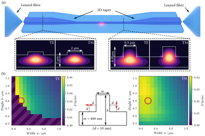
To conveniently couple the light in and out of the waveguide chip, we chose silica core single mode lensed fibers (S630-HP) with a spot diameter of (OZ Optics). Due to the mismatch between the fiber’s spot size and the dimensions of the mode in the emitter coupling region of the waveguide (sub-micron) we designed a mode-size converter. The inverse tapers usually employed in strip waveguides for mode conversion Almeida et al. (2003) are not feasible for our rib waveguide structure due to the requirement of the supporting membrane, therefore a two-dimensional (2D) section of the waveguide is tapered both laterally and vertically, as illustrated in Fig. 2(a). This tapered section acts as an adiabatic mode size converter and increases the on- and off-chip coupling efficiency with the single mode fibers. The fundamental TE and TM eigenmode profiles at a wavelength of before and after the 2D tapered section are shown in the lower part of Fig. 2(a). The eigenmode solutions are obtained from a frequency-domain guided-mode solver (JCMwave). When calculating the overlap of the guided mode in the waveguide and the spot diameter of the lensed fiber, we can find a power coupling of and without the tapered waveguide section for TE and TM polarization respectively. When the waveguide size is increased by a 2D taper, the power coupling to the fundamental mode is increased to and for TE and TM, respectively.
To experimentally estimate the on-chip coupling efficiency, we used a laser with an emission wavelength of , which was coupled into the waveguide from one side with the lensed fiber and collected the guided light on the other side of the waveguide chip with an objective lens. The lensed fiber was mounted with a V-groove fiber holder, coarse and fine positioning was performed with a XYZ linear translation stage (Thorlabs) and a XYZ piezo positioning stage (PiezoJena) respectively. After careful optimization of the fibers position with respect to the waveguide, the transmitted light is recorded on a photodetector and its power is compared with the laser power measured directly behind the lensed fiber. A fiber beam splitter is used to generate a power reference signal in order to take into account fluctuations in laser power within the fiber. In addition, transmitted light polarization can be adjusted with an inline fiber polarization controller to be mainly TE or TM polarized. The ratio of transmitted light to incident light can then be used as lower bound for on-chip coupling efficiency, assuming zero losses within the waveguide and tapered sections.
Each waveguide chip was fabricated containing a variety of waveguides with different dimensions. A total of 14 waveguides with 2D tapers and dimensions comparable to those in Fig. 2(a) were tested, and apart from some outliers likely due to defects in these waveguides, the average total measured transmission was for both incident polarization angles. The deviation of the calculated power coupling value from the experimentally obtained values for transmission is most likely due to a combination of losses, the imperfect orientation of the fiber with respect to the waveguide and propagation losses within the waveguide. We would like to emphasize that we did not observe significant differences comparing transmission measurements done with tapered and untapered waveguides, hence we assume that tapering of the waveguides does not lead to notable additional losses.
The interaction efficiency of the emitter with the guided modes in the waveguide can be described by the factor, defined by the fraction of the total emitted energy which is coupled to the guided mode , where denotes the emitters decay rate into the guided modes of the waveguide and the emitter’s total decay rate. The factor can be obtained from performing a full 3D simulation of the waveguide structure with a radiating dipole emitter where the output into the guided mode is monitored. To facilitate the problem, we exploit the possibility of calculating the coupling Purcell factor for a point-like dipolar emitter from a simple 2D simulation of the guided modes as described by Barthez et al. Barthes et al. (2011):
| (1) |
where denotes the undisturbed decay rate of the emitter (in vacuum), is a normalized vector pointing in direction of propagation along the waveguide which is normal to the surface , is the absolute value of the photon momentum in air and denotes the electric field components parallel to the dipole orientation of an emitter. The layout for the simulation can be found in the center of Fig. 2(b) where the dipole emitter was placed either vertical or horizontal in respect to the waveguide structure from each side of the inner edge.
In order to calculate from a 3D calculation of the same structure is carried out, from which the total emitted power of the radiating dipolar point source sitting next to the waveguide is obtained as well as the total emitted power in vacuum. By combining the results of the 2D simulation which gives us and the 3D simulation from which we obtain we can then calculate as:
| (2) |
The dimensions where is optimal are found by a parameter scan of the height and width of the waveguide. In the scan the thickness of the membrane was set constant to a value of where a robust fabrication and handling of the integrated structures was still ensured and the wavelength was set to as this is approximately the peak of the NV centers emission. The nanometer-sized diamonds chosen for integration typically have a diameter of and the NV center was assumed to be located at the center of the nanocrystal. The factor for the fundamental TE (TM) guided mode coupling to a horizontal (vertical) dipole emitter from the inner edges can be found in Fig. 2(b) left (right). As TE modes become no longer strongly guided and therefore very lossy for smaller dimensions of the waveguide was set to zero here and the area is marked shaded.
The final device was designed to support both the fundamental TE and TM mode due to the random orientation of the NV centers dipole axis, so we chose a width , height and membrane thicknesses , marked with red circles in Fig. 2(b). The simulated factor for a device with these dimensions is for a horizontally oriented dipole coupling to the TE mode and for a vertical oriented dipole coupling to the TM mode in the waveguide, with corresponding values of and for the coupling Purcell factor.
As shown in Fig. 2(b), a device with a higher aspect ratio could only marginally improve coupling efficiency, so the fabrication of such a device was not pursued. On the other hand, it is possible to significantly increase the coupling efficiency by reducing the membrane height, which improves access to the guided mode but decreases mechanical stability. A detailed discussion on increasing coupling efficiency can be found in Section IV.
III Results of the assembled device

For functionalization, samples with multiple straight waveguides and dimensions as derived in the last section ( in the coupling area) were fabricated and characterized. A waveguide was then selected and functionalized with a preselected single NV center hosted in a nanometer sized diamond, as described in subsection II.1 . After AFM manipulation, the presence of the NV center is verified in an all-confocal configuration where the the continuous wave pump laser is focused onto the sample using a objective lens (Olympus, MPLAPON60X). The reflected light is spectrally filtered by two longpass filters (Omega optics) and spatially by a pinhole. The remaining fluorescence is directed either onto two avalanche photo diodes (APDs; Perkin-Elmer) in a Hanbury Brown and Twiss (HBT) configuration to verify the single photon generation, a CCD camera or a spectrometer. In the confocal scan, the NV center can be identified as a bright fluorescent spot near the waveguide (see upper part of Fig. 3(a)). The lower part of Fig. 3(a) shows the resulting second order correlation, measured with the HBT setup. Fitting the autocorrelation data to a three-level model:
| (3) |
where denotes the bunching amplitude, the antibunching time and the bunching time, we obtained a value of for this confocal excitation and detection scheme, which was limited by the APDs dark counts, its timing resolutions, and possible fluorescent background caused by residual graphite on the nanocrystal’s surface.
The bright spot approximately left of the NV center does not originate from NV fluorescence as determined from the photon statistics, it most likely is some broken off part of the AFM tip used to position the NV center. Fortunately, this scatterer does not have a negative influence on the performance of the device.
To verify the coupling of the waveguide mode to the NV center, we couple the green pump laser to one input port of the waveguide via a lensed fiber and use the confocal microscope only to detect the resulting fluorescence. By scanning the confocal detection over the sample, the fluorescence map in Fig. 3(b) is recorded, which shows that no background fluorescence of the waveguide can be detected even with strong pumping ( after the lensed fiber). The autocorrelation data originating from the bright spot reveals a , which is comparable to the obtained during confocal excitation of the NV center, verifying that the NV center can also efficiently be excited via the waveguide without increasing background fluorescence, thanks to the excellent optical properties of the SiO2.
In a third configuration, the NV center is optically pumped via the microscope objective and the NV fluorescence directly coupled to the waveguide is detected by off-chip coupling the light from both waveguide ends to single-mode fibers. The remaining pump light is filtered out by a single longpass filter at the end of each fiber before being detected by two APDs. Fig. 3(c) shows the fluorescence map detected from one output arm of the waveguide when scanning the laser over the waveguide and NV. In this configuration the waveguide itself acts as an intrinsic beamsplitter. Here the autocorrelation function recorded between the two output arms shows an anti-bunching with clearly indicating the mainly single-photon characteristics of the guided light in the waveguide.
Next, we assess the experimentally achieved dipole-waveguide coupling efficiency through the comparison of the fluorescence counts detected in the confocal and waveguide configurations, each corrected for its respective coupling efficiency and transmission efficiency :
| (4) |
Our confocal setup has an overall collection efficiency of (fraction of dipole emission collected by the objective lens , transmittance of optical elements ) and provides typical count rates of from single NV centers Pyrlik et al. (2019). The integrated waveguide system has a transmission of and provides total count rates of per output arm. Given that the total counts emitted by the NV stays the same in both situations, rearranging Eq. 4 results in a NV-waveguide coupling efficiency of
| (5) |
This derived coupling efficiency fits very well to the simulated values of () for a horizontally (vertically) oriented dipole emitter coupling to the TE (TM) mode in the waveguide.
IV Increasing coupling efficiency
For demanding applications, e.g. the experimental realization of a single photon non-linear device Kewes et al. (2016), an increased coupling efficiency between emitter and guided mode would be desirable. In the following we will comment on some prospects for increasing the coupling efficiency far beyond the theoretical value of of our fabricated device, but at the same time have higher manufacturing and/or assembly requirements.
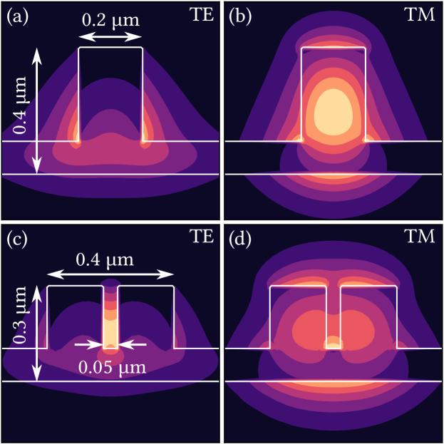
In principle, it is crucial to obtain better access to the guided mode in the waveguide, i.e. smaller waveguide dimensions, in order to make the evanescent field more accessible. In subsection II.2 we have already optimized the dimensions of the waveguide, but with a very conservative thickness of the supporting membrane () to ensure a very robust device. If, for example, the membrane thickness is reduced to , parameter scans yield the optimal dimensions of the waveguide ( and , see Fig. 4(a,b)) which allows an increased factor of () for a vertical (horizontal) dipole emitter coupling to the guided TE (TM) mode.
In order to improve the coupling efficiency even further, a slot-waveguide could be implemented. Here, the supported mode channels most of the electromagnetic field within the slot, allowing optimal access to the guided mode when the emitter is placed in the slot. In Fig. 4(c,d) we show an optimized design for a slot-waveguide with a slot width of and a membrane thickness of . This design is more difficult to fabricate and functionalize, but would also result in an greatly increased factor of () for a vertical (horizontal) dipole emitter located in the center of the slot and coupling to the TE (TM) guided mode.
A further increase of the coupling efficiency could be achieved e.g. by using an even thinner membrane or an even smaller slot width. It should be noted, that this requires even higher fabrication, assembly and handling demands, as the device becomes more fragile. Another prospect for increasing the coupling efficiency could be more complex systems, e.g. overgrowing the emitter with SiO2 after positioning it or an adiabatic coupling of the dipole emitter to the waveguide Patel et al. (2016); Davanco et al. (2017).
V Conclusion and outlook
In summary, we present on-chip SiO2 photonic structures with ultra-low fluorescence at visible wavelengths which are very well suited for the integration of solid state single-photon emitters that require relatively high excitation powers, such as the NV center. The integrated structure allows effective routing of excitation laser sources and single photons via a freestanding rib-waveguide configuration. The on- and off-chip power coupling efficiency to single mode fibers can be increased by introducing 2D tapered sections of the waveguide to adiabatically transform the size of the guided mode. By deterministically positioning a nanodiamond with a single NV center in close proximity to the waveguide, we were able to demonstrate single photon generation by either pumping the NV center over the waveguide and detection in free-space, or by pumping over the microscope objective and detection of the photons coupled to the single guided mode of the waveguide. We could also experimentally verify the theoretically predicted NV-waveguide coupling efficiency. Furthermore we presented and commented on possible ways to enhance the theoretical coupling efficiency between the guided mode and the quantum emitter by over one order of magnitude.
The device and functionalization presented here is not limited to NV centers in diamond, but can also be transferred to other solid-state quantum emitters in the visible, such as other defect centers in diamond or defects in 2D materials. Furthermore, the integrated device can be extended with other on-chip photonic structures such as high-Q ring resonators Pyrlik et al. (2019), directional couplers, on-chip detectors Ferrari et al. (2018), and microwave antennas which allows for the monolithic realization of complex devices consisting of various functionalities, e.g. the optical microintegration of those chips with high functional density together with light sources, detectors, and electronics.
In this way, the presented photonic platform and integration technique opens up the possibility of building up complex structures with several integrated functionalities. Even the packaging of the chip and pump laser diodes within an optical module can be envisioned. This would be highly attractive for compact modules for integrated quantum technologies.
VI Acknowledgments
We thank Günter Kewes and Bernd Sontheimer for fruitful discussions. We acknowledge financial support by the European Fund for Regional Development of the European Union in the framework of project iMiLQ, administrated by the Investitionsbank Berlin within the Program to Promote Research, Innovation, and Technologies (ProFIT) under grant 10159465 and the Federal Ministry of Education and Research of Germany in the framework of Q.Link.X (project number 16KIS0876).
References
- Aharonovich and Neu (2014) I. Aharonovich and E. Neu, Advanced Optical Materials 2, 911 (2014).
- Gruber et al. (1997) A. Gruber, A. Dräbenstedt, C. Tietz, L. Fleury, J. Wrachtrup, and C. Von Borczyskowski, Science 276, 2012 (1997).
- Togan et al. (2010) E. Togan, Y. Chu, A. S. Trifonov, L. Jiang, J. Maze, L. Childress, M. V. G. Dutt, A. S. Sørensen, P. R. Hemmer, A. S. Zibrov, and M. D. Lukin, Nature 466, 730 (2010).
- Maurer et al. (2012) P. C. Maurer, G. Kucsko, C. Latta, L. Jiang, N. Y. Yao, S. D. Bennett, F. Pastawski, D. Hunger, N. Chisholm, M. Markham, D. J. Twitchen, J. I. Cirac, and M. D. Lukin, Science 336, 1283 (2012).
- Kurtsiefer et al. (2000) C. Kurtsiefer, S. Mayer, P. Zarda, and H. Weinfurter, Physical Review Letters 85, 290 (2000).
- Thiering and Gali (2018) G. Thiering and A. Gali, Physical Review X 8, 021063 (2018).
- Lühmann et al. (2018) T. Lühmann, N. Raatz, R. John, M. Lesik, J. Rödiger, M. Portail, D. Wildanger, F. Kleißler, K. Nordlund, A. Zaitsev, J.-F. Roch, A. Tallaire, J. Meijer, and S. Pezzagna, Journal of Physics D: Applied Physics 51, 483002 (2018).
- Tran et al. (2016) T. T. Tran, K. Bray, M. J. Ford, M. Toth, and I. Aharonovich, Nature Nanotechnology 11, 37 (2016).
- Kimble (2008) H. J. Kimble, Nature 453, 1023 (2008).
- Benson (2011) O. Benson, Nature 480, 193 (2011).
- Schröder et al. (2012) T. Schröder, M. Fujiwara, T. Noda, H.-Q. Zhao, O. Benson, and S. Takeuchi, Optics Express 20, 10490 (2012).
- Liebermeister et al. (2014) L. Liebermeister, F. Petersen, A. v. Münchow, D. Burchardt, J. Hermelbracht, T. Tashima, A. W. Schell, O. Benson, T. Meinhardt, A. Krueger, A. Stiebeiner, A. Rauschenbeutel, H. Weinfurter, and M. Weber, Applied Physics Letters 104, 031101 (2014).
- Fujiwara et al. (2016) M. Fujiwara, K. Yoshida, T. Noda, H. Takashima, A. W. Schell, N. Mizuochi, and S. Takeuchi, Nanotechnology 27, 455202 (2016).
- Patel et al. (2016) R. N. Patel, T. Schröder, N. Wan, L. Li, S. L. Mouradian, E. H. Chen, and D. R. Englund, Light: Science & Applications 5, e16032 (2016).
- Schell et al. (2017) A. W. Schell, H. Takashima, T. T. Tran, I. Aharonovich, and S. Takeuchi, ACS Photonics 4, 761 (2017).
- Shi et al. (2016) Q. Shi, B. Sontheimer, N. Nikolay, A. W. Schell, J. Fischer, A. Naber, O. Benson, and M. Wegener, Scientific Reports 6, 31135 (2016).
- Schnauber et al. (2018) P. Schnauber, J. Schall, S. Bounouar, T. Höhne, S.-I. Park, G.-H. Ryu, T. Heindel, S. Burger, J.-D. Song, S. Rodt, and S. Reitzenstein, Nano Letters 18, 2336 (2018).
- Faraon et al. (2011) A. Faraon, P. E. Barclay, C. Santori, K.-M. C. Fu, and R. G. Beausoleil, Nature Photonics 5, 301 (2011).
- Burek et al. (2017) M. J. Burek, C. Meuwly, R. E. Evans, M. K. Bhaskar, A. Sipahigil, S. Meesala, B. Machielse, D. D. Sukachev, C. T. Nguyen, J. L. Pacheco, E. Bielejec, M. D. Lukin, and M. Lončar, Physical Review Applied 8, 024026 (2017).
- Bhaskar et al. (2017) M. K. Bhaskar, D. D. Sukachev, A. Sipahigil, R. E. Evans, M. J. Burek, C. T. Nguyen, L. J. Rogers, P. Siyushev, M. H. Metsch, H. Park, F. Jelezko, M. Lončar, and M. D. Lukin, Physical Review Letters 118, 223603 (2017).
- Gschrey et al. (2013) M. Gschrey, F. Gericke, A. Schüßler, R. Schmidt, J.-H. Schulze, T. Heindel, S. Rodt, A. Strittmatter, and S. Reitzenstein, Applied Physics Letters 102, 251113 (2013).
- Zadeh et al. (2016) I. E. Zadeh, A. W. Elshaari, K. D. Jöns, A. Fognini, D. Dalacu, P. J. Poole, M. E. Reimer, and V. Zwiller, Nano Letters 16, 2289 (2016).
- Gould et al. (2016) M. Gould, E. R. Schmidgall, S. Dadgostar, F. Hatami, and K.-M. C. Fu, Physical Review Applied 6, 011001 (2016).
- Kim et al. (2017) J. H. Kim, S. Aghaeimeibodi, C. J. Richardson, R. P. Leavitt, D. Englund, and E. Waks, Nano Letters 17, 7394 (2017).
- Tonndorf et al. (2017) P. Tonndorf, O. Del Pozo-Zamudio, N. Gruhler, J. Kern, R. Schmidt, A. I. Dmitriev, A. P. Bakhtinov, A. I. Tartakovskii, W. Pernice, S. Michaelis de Vasconcellos, and R. Bratschitsch, Nano Letters 17, 5446 (2017).
- Mouradian et al. (2015) S. L. Mouradian, T. Schröder, C. B. Poitras, L. Li, J. Goldstein, E. H. Chen, M. Walsh, J. Cardenas, M. L. Markham, D. J. Twitchen, M. Lipson, and D. Englund, Physical Review X 5, 031009 (2015).
- Davanco et al. (2017) M. Davanco, J. Liu, L. Sapienza, C.-Z. Zhang, J. V. De Miranda Cardoso, V. Verma, R. Mirin, S. W. Nam, L. Liu, and K. Srinivasan, Nature Communications 8, 889 (2017).
- Kewes et al. (2016) G. Kewes, M. Schoengen, O. Neitzke, P. Lombardi, R.-S. Schönfeld, G. Mazzamuto, A. W. Schell, J. Probst, J. Wolters, B. Löchel, C. Toninelli, and O. Benson, Scientific Reports 6, 28877 (2016).
- Siampour et al. (2017) H. Siampour, S. Kumar, and S. I. Bozhevolnyi, ACS Photonics 4, 1879 (2017).
- Siampour et al. (2018) H. Siampour, S. Kumar, V. A. Davydov, L. F. Kulikova, V. N. Agafonov, and S. I. Bozhevolnyi, Light: Science & Applications 7, 61 (2018).
- Chen et al. (2012) P. Chen, Y. Zhu, Y. Shi, D. Dai, and S. He, Optics express 20, 22531 (2012).
- Pyrlik et al. (2019) C. Pyrlik, J. Schlegel, F. Böhm, A. Thies, O. Krüger, O. Benson, A. Wicht, and G. Tränkle, IEEE Photonics Technology Letters 31, 479 (2019).
- Schell et al. (2011) A. W. Schell, G. Kewes, T. Schröder, J. Wolters, T. Aichele, and O. Benson, Review of Scientific Instruments 82, 073709 (2011).
- Ferrari et al. (2018) S. Ferrari, C. Schuck, and W. Pernice, Nanophotonics 7, 1725 (2018).
- Thies (2018) A. Thies, unpublished (2018).
- Almeida et al. (2003) V. R. Almeida, R. R. Panepucci, and M. Lipson, Optics Letters 28, 1302 (2003).
- Barthes et al. (2011) J. Barthes, G. Colas Des Francs, A. Bouhelier, J. C. Weeber, and A. Dereux, Physical Review B - Condensed Matter and Materials Physics 84, 1 (2011).