Towards Surface Diffusion Potential Mapping on Atomic Length Scale
Abstract
The surface diffusion potential landscape plays an essential role in a number of physical and chemical processes such as self-assembly and catalysis. Diffusion energy barriers can be calculated theoretically for simple systems, but there is currently no experimental technique to systematically measure them on the relevant atomic length scale. Here, we introduce an atomic force microscopy based method to semi-quantitatively map the surface diffusion potential on an atomic length scale. In this proof of concept experiment, we show that the atomic force microscope damping signal at constant frequency-shift can be linked to non-conservative processes associated with the lowering of energy barriers and compared with calculated single-atom diffusion energy barriers.
I Introduction
The behaviour of adspecies deposited on a surface is crucial for physico-chemical surface processes such as catalysis Over et al. (2000); Somorjai et al. (2006); Chen and Rodionov (2016); Jones et al. (2016), surface decoration Dvořák et al. (2016) and self-assembly Barth, Costantini, and Kern (2005) to name a few. For example, the emerging field of single-atom catalysts is currently facing two grand challenges: the proper surface decoration with single-atom adsorbates Zhu et al. (2017) and the anchoring stability (low diffusion) of the single-atom catalysts at the atomic level Liu (2016); Chen et al. (2017). Therefore, a good understanding of the surface diffusion potential is desirable for the adequate tuning of such processes.
As adspecies diffuse on a surface, they ultimately relax at local minima known as the adsorption sites. For a given stabilized adspecies, the minimum energy differences between these sites, preventing any further diffusion, are known as the potential energy barriers (or activation energies). Such barriers can be overcome globally, by increasing the adspecies energy with temperature Roder et al. (1993), or locally by lowering the confining barrier with, for instance, a scanning probe tip (stimulated diffusion) Sugimoto et al. (2005).
Here, we focus on scanning probe microscopy techniques which have been used to characterize the surface diffusion of atoms and molecules on metals, Ehrlich and Hudda (1966); Ehrlich (1980); Gomer (1990); Gravil et al. (1996); Barth (2000); Ternes et al. (2008); Hedgeland et al. (2016) insulators Gravil et al. (1996); Repp et al. (2004); Sonnleitner et al. (2011); Repp et al. (2016) and semiconductors Suliga and Henzler (1983); Song et al. (2016). Two main approaches have been adopted for determining associated energy barriers. In the first method, the adspecies thermally diffuse and their positions are tracked in time sequenced topographic images Gomer (1990) or with an atom-tracking technique Swartzentruber (1996). These images allow to calculate the hopping rates at different temperatures via an Arrhenius analysis. However, this method is very time consuming, and the diffusion of specific individual adsorbates can be hard to track. The second approach is known as the onset method, where the energy barriers are obtained from an assumed growth model and experimentally observed island coverage Bott et al. (1996); Loske et al. (2010). More recently, several alternative methods have been proposed: non thermal diffusion stimulated by a tip probe (e.g. by inelastic excitations) Sonnleitner et al. (2011), mapping the diffusion potential by means of the local electric field of a scanning tunneling microscope (STM) Shi-Chao et al. (2012), and determining the kinetic pathways of adatoms and vacancies by aberration-corrected transmission electron microscopy Hong et al. (2017).
Scanning probes are routinely used to characterize structural, electronic and mechanical surface properties via imaging, spectroscopy and indentation. Significant progress has been made identifying and moving individual atoms along the surface with atomic force microscopy (AFM) and STM Custance, Perez, and Morita (2009); Hla (2014). However, there is no experimental work mapping the surface diffusion potential by shifting a known single atom along the surface. This is because of the lack of an obvious direct way to extract the diffusion energy barriers from a scanning probe observable. In AFM, dissipative interactions due to internal losses in the force sensor or due to the tip-sample interaction, are accessible through recording the cantilever damping signal Pishkenari (2015). In the absence of structural changes on the tip, contrast in the damping channel can be associated with atomic dynamic processes on the surface which lead to energy dissipation. For example, it has been shown recently that diffusion energy barriers can be estimated from the force sensor’s dissipated energy when reshaping C60 nanostructures Freund et al. (2016). The relation between tip stimulated diffusion and the energy dissipation has also been discussed in the case of Si adatoms on Si(111) Arai et al. (2018). Using a conducting AFM setup allows to compensate the contact potential, thus preventing electrostatic forces which could trigger undesirable charge related effects.
It is known that on metal and semiconductor surfaces, adatom diffusion can be stimulated by the AFM tip through a lowering of the energy barriers Kürpick and Rahman (1999); Custance, Perez, and Morita (2009) due to the chemical reactivity of the tip with the adatom Sugimoto et al. (2008, 2013, 2014); Yurtsever et al. (2017). Theoretical calculations have demonstrated that the presence of the tip does indeed lower the diffusion barriers and can promote directed diffusion by trapping the adatom, also known as atom gating Enkhtaivan and Oshiyama (2017). In the case of the reconstructed Si(001) surface, flipping of the buckled Si dimers driven by a tip induced lowering of the energy barrier is a well-known dissipation channel in AFM imaging Perez et al. (1999); Kantorovich and Hobbs (2006); Sweetman et al. (2011); Bamidele et al. (2012). Naturally, such structural surface modifications are accompanied by atomic scale modifications of the diffusion barriers.
Here, we discuss two schemes to access element specific surface diffusion energy barriers by mapping the energy dissipated in the sensor of an AFM. We start by showing how we can probe the diffusion barriers in constant frequency shift () AFM images of self-assembled Mn chains on reconstructed Si(001) by using the Si dimer flipping as a reference. We then focus on the characteristic features in the damping channel during stimulated diffusion of a single Mn atom on reconstructed Si(001). All experiments discussed here were performed at 78 K, thus the condition (: activation energy) preventing spontaneous adatom diffusion is valid and we assume (: dissipated energy) for tip stimulated single-atom diffusion. We analyze the damping signal by using the well-known Si dimer flip as a reference to compare with other dissipative processes, thus avoiding any assumption regarding the tip other than a stable apex. Using the Si dimer flip as a reference enables the semi-quantitative analysis proposed here. Without such a reference, a very large data set would be required to average out the dependence of the damping signal on the atomistic structure of the tip apex, which is usually not known in details.
II Experimental Methods
Manganese atoms were deposited in-situ on clean p-type (boron doped, 0.1 cm) reconstructed Si(001) surfaces. The deposition was performed in UHV (base pressure 10-11 mbar) at room temperature prior to the STM/AFM investigations. All STM/AFM micrographs reported here were obtained in UHV at 78 K using an Omicron LT-STM. We used qPlus sensors with electrochemically etched W tips and a resonance frequency of kHz. The sensor is equipped with a separate wire for tunneling current to avoid cross-talk. The tip oxide is first removed by scanning the Au(111) surface, followed by controlled tip crashes on Si(001) which very likely lead to a Si tip apex. All STM topographies were acquired in constant , while all AFM topographies were taken in constant , with a constant oscillation amplitude 560 pm and with zero bias.
III Results and Discussion
Fig. 1(a) is an AFM topographic image of the Si(001) surface with a single Mn chain running diagonally through the frame. The image was acquired at a constant = -9.7 Hz. The Mn atoms in the chain appear blurred, seemingly occupying two sites in the chain structure. This behaviour is unexpected and indicative of atom manipulation Trevethan et al. (2007). Indeed, high resolution STM imaging of stable Mn chains is routinely obtained at 78 K Villarreal et al. (2015) and Mn chains are thermodynamically stable below room temperature (break up has been reported in chains heated to 115∘C Nolph et al. (2010)). High resolution imaging of the Mn chains is also possible by AFM at an approriate feedback loop setting Villarreal et al. (2015). The motion of each Mn atom composing the chain in Fig. 1(a) is driven by the AFM tip as a result of an increased tip-surface interaction. The latter is known to trigger flipping of the Si dimers on the Si(001) surface at 78 K, in particular when sitting over the down Si of the buckled Si dimers Kantorovich and Hobbs (2006). The energy driving this flipping is supplied by the AFM tip and manifests itself as an increased dissipation when the tip is passing over the down Si atom. Similarly, the increased dissipation signal observed in Fig. 1(b) when the tip is passing over the Mn chain is a consequence of the AFM tip induced switching of the Mn atom positions between the H’A and H’B sites (Fig. 1(c)). Hence, the contrast in Fig. 1(b) can be considered as a measure of the energy required to move Mn atoms within the chain structure. Note that the movement is determined by the local atomic structure and not the scan direction, suggesting the possibility to extract information about the surface diffusion potential.
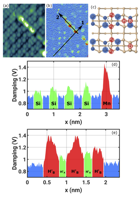
The damping signal can be analyzed more quantitatively by comparison to theoretical calculations of the energy required to induce switching of buckled Si dimers. The latter is estimated by density functional theory (DFT) to be in the range of 100-255 meV for hole doped Si(001) Ren et al. (2016). Fig. 1(b) and the profiles in Figs. 1(d) and 1(e) show that the AFM damping amplitude is similar at the Mn H’A sites and over the Si-down sites. In agreement with this observation, theoretical calculations find an energy barrier of the order of 160 meV Wang et al. (2010); Villarreal et al. (2015) to move a Mn atom from its stable H’A site in the chain to the H’B site. This correspondence provides justification to use the AFM damping signal as a measure of the surface diffusion potential. When positioned over the unstable H’B site of this particular Mn chain, the AFM tip is subject to a significant larger damping. Although better statistics are needed for a robust quantitative analysis, our experiment suggests an increase of the order of 30 of the dissipation over the H’B site in comparison to the H’A site, a number to be compared with future theoretical simulations.
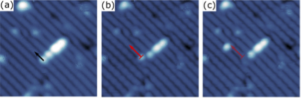
So far, we have demonstrated that the AFM damping signal contributes to understanding the stability of a self-assembled atomic structure. However, we still gain no insight on the chain formation dynamics. To this end, we propose to explore the stimulated diffusion of an isolated Mn atom combining AFM manipulation and STM imaging. The idea is to measure the local AFM dissipation while dragging a single Mn atom along the bare Si(001) surface. To be sure we are indeed moving a Mn atom, we start by extracting one from an existing Mn chain following the sequence illustrated in Fig. 2. First, we identify a short Mn chain in a STM micrograph (Fig. 2(a)). Next, we proceed with an AFM manipulation in the direction of the black arrow at constant f = -28.6 Hz to isolate one apex Mn atom (Fig. 2(b)). This individual Mn atom is then moved further away (Fig. 2c) along the red arrow in Fig. 2(b) at f = -28 Hz. The latter AFM manipulation path away from any chain provides valuable insight on the diffusion potential of Mn single atoms along the clean Si(001) surface (Fig. 3).
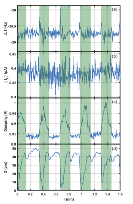
During the AFM tip stimulated diffusion, the Mn atom moves along the center of the Si dimer row to a location different from its stable H’ edge position in the Mn chain. Three sites are compatible with the STM contrast of the isolated Mn atom in Fig. 2(c), where the dark grooves correspond to the center of the Si(001) dimer rows: Sena and Bowler (2011) the H site between two Si dimers, the dimer vacancy filling D site, or the short bridge B site above a Si dimer (see Fig. 1(c)). The best agreement with DFT simulated STM images is found for the B site, although energetically it is 500 meV less favorable than the H’ site Wang et al. (2010). Further details about the diffusion process can be inferred from the AFM response during the Mn atom motion (Fig. 3). The atom manipulation is done at constant frequency shift (Fig. 3(a)) and the tunneling current, monitored simultaneously with a low bias voltage applied to the conducting AFM tip to compensate the local contact potential, is featureless (Fig. 3(b)). Meanwhile, the AFM dissipation (Fig. 3(c)) and amplitude (Fig. 3(d)) reveal strong periodic variations, whose periodicities correspond to the Si dimer spacing (3.8 Å).
The AFM traces in Fig. 3 provide compelling evidence that the stimulated diffusion process is driven by force interactions between the tip and the Mn atom. The increased dissipation highlighted in green in Fig. 3(c) is unambiguously linked to the local reduction of the energy barrier to move the Mn atom past each Si dimer, as described in ref Sugimoto et al. (2014). It is indeed only observed when moving a Mn atom along the surface, never while scanning the bare Si(001) surface using the same settings. These dissipation peaks are not compatible with Si dimer flipping, which should only occur every second Si dimer, when the AFM tip is passing over a down Si atom along the red arrow in Fig. 2(c). Although we cannot image the Mn atom during the tip induced diffusion, the shape and relative phases of the AFM traces in Fig. 3 provide some information on the diffusion process itself. The dissipation signal in Fig. 3(c) peaks just before the tip drops by about 50 pm towards the surface in Fig. 3(d). Because we observe the same Z deflection amplitude of the AFM tip when imaging a stable Mn adatom on the Si(001) surface, the tip extension most likely corresponds to the Mn atom jumping away from under the tip. The measured dissipation is similar to the Mn atom on the H’ site in the chain and to the Si dimer, providing the basis for future quantitative theoretical modeling.
The multichannel signature in Fig. 3 shows that the Mn atom is being dragged by the AFM tip from H’ to B via non-equivalent sites. This is in agreement with theoretical predictions of the lowest energy path for a Mn atom diffusing along the Si dimer row Wang et al. (2010); Hortamani et al. (2006). Attempting to move the Mn atom perpendicular to the Si-dimer rows was very erratic and mostly failed. The above observations suggest Mn atoms are primarily diffusing along the Si dimer rows during the self-assembly process, with a vanishing probability of diffusing perpendicular to them. Such a unidirectional surface diffusion potential landscape can explain the limited length of self-assembled Mn chains, as observed in experiments.
IV Conclusion
In summary, we describe a proof of principle to map the surface diffusion potential of Mn on the clean Si(001) reconstructed surface by measuring the position dependent dissipation of an AFM cantilever during the tip stimulated diffusion of Mn atoms. While theoretical input is required to describe the exact atomistic mechanisms involved in this stimulated diffusion process, some quantitative insight is possible by comparing with the dissipation associated with the well-documented tip induced Si dimer flipping. The experiment shows that Mn is preferably diffusing along the center of the Si(001) dimer rows, with a potential barrier preventing diffusion perpendicular to the dimer rows. This strong anistropy can explain the limited length of self-assembled Mn chains on the Si(001) surface, since additional Mn atoms can only be supplied along a single Si dimer row closest to the Mn chain apex. The generic scheme introduced here can be extended to other adsorbate/surface systems, allowing an original and potentially quantitative insight on adsorption and self-assembly processes.
Acknowledgements.
We thank G. Manfrini and A. Guipet for their technical assistance. C. R., R. V. and A. S. acknowledge support from the Swiss National Science Foundation through division 2 and C. J. K. acknowledges financial support from a UCL Impact Studentship.References
- Over et al. (2000) H. Over, Y. D. Kim, A. Seitsonen, S. Wendt, E. Lundgren, M. Schmid, P. Varga, A. Morgante, and G. Ertl, “Atomic-scale structure and catalytic reactivity of the ruo2 (110) surface,” Science 287, 1474–1476 (2000).
- Somorjai et al. (2006) G. A. Somorjai, K. M. Bratlie, M. O. Montano, and J. Y. Park, “Dynamics of surface catalyzed reactions; the roles of surface defects, surface diffusion, and hot electrons,” J. Phys. Chem. B 110, 20014–20022 (2006).
- Chen and Rodionov (2016) T. Chen and V. O. Rodionov, “Controllable catalysis with nanoparticles: Bimetallic alloy systems and surface adsorbates,” ACS Catalysis 6, 4025–4033 (2016).
- Jones et al. (2016) J. Jones, H. Xiong, A. T. DeLaRiva, E. J. Peterson, H. Pham, S. R. Challa, G. Qi, S. Oh, M. H. Wiebenga, X. I. Pereira Hernández, Y. Wang, and A. K. Datye, “Thermally stable single-atom platinum-on-ceria catalysts via atom trapping,” Science 353, 150–154 (2016).
- Dvořák et al. (2016) F. Dvořák, M. F. Camellone, A. Tovt, N.-D. Tran, F. R. Negreiros, M. Vorokhta, T. Skála, I. Matolínová, J. Mysliveček, V. Matolín, and S. Fabris, “Creating single-atom pt-ceria catalysts by surface step decoration,” Nat. Commun. 7, 10801 (2016).
- Barth, Costantini, and Kern (2005) J. V. Barth, G. Costantini, and K. Kern, “Engineering atomic and molecular nanostructures at surfaces,” Nature 437, 671 (2005).
- Zhu et al. (2017) C. Zhu, S. Fu, Q. Shi, D. Du, and Y. Lin, “Single-atom electrocatalysts,” Angew. Chem., Int. Ed. (2017).
- Liu (2016) J. Liu, “Catalysis by supported single metal atoms,” ACS Catalysis 7, 34–59 (2016).
- Chen et al. (2017) Y. Chen, Z. Huang, Z. Ma, J. Chen, and X. Tang, “Fabrication, characterization, and stability of supported single-atom catalysts,” Catal. Sci. Technol. 7, 4250–4258 (2017).
- Roder et al. (1993) H. Roder, E. Hahn, H. Brune, J.-P. Bucher, and K. Kern, “Building one-dimensional and 2-dimensional nanostructures by diffusion-controlled aggregation at surfaces,” Nature 366, 141–143 (1993).
- Sugimoto et al. (2005) Y. Sugimoto, M. Abe, S. Hirayama, N. Oyabu, O. Custance, and S. Morita, “Atom inlays performed at room temperature using atomic force microscopy,” Nat. Mater. 4, 156–159 (2005).
- Ehrlich and Hudda (1966) G. Ehrlich and F. Hudda, “Atomic view of surface self-diffusion: Tungsten on tungsten,” J. Chem. Phys. 44, 1039–1049 (1966).
- Ehrlich (1980) G. Ehrlich, “Quantitative examination of individual atomic events on solids,” J. Vac. Sci. Technol. 17, 9–14 (1980).
- Gomer (1990) R. Gomer, “Diffusion of adsorbates on metal surfaces,” Rep. Prog. Phys. 53, 917 (1990).
- Gravil et al. (1996) P. Gravil, M. Devel, P. Lambin, X. Bouju, C. Girard, and A. Lucas, “Adsorption of c60 molecules,” Phys. Rev. B 53, 1622 (1996).
- Barth (2000) J. V. Barth, “Transport of adsorbates at metal surfaces: from thermal migration to hot precursors,” Surf. Sci. Rep. 40, 75–149 (2000).
- Ternes et al. (2008) M. Ternes, C. P. Lutz, C. F. Hirjibehedin, F. J. Giessibl, and A. J. Heinrich, “The force needed to move an atom on a surface,” Science 319, 1066–1069 (2008).
- Hedgeland et al. (2016) H. Hedgeland, M. Sacchi, P. Singh, A. J. McIntosh, A. P. Jardine, G. Alexandrowicz, D. J. Ward, S. J. Jenkins, W. Allison, and J. Ellis, “Mass transport in surface diffusion of van der waals bonded systems: Boosted by rotations?” J. Phys. Chem. Lett. 7, 4819–4824 (2016).
- Repp et al. (2004) J. Repp, G. Meyer, F. E. Olsson, and M. Persson, “Controlling the charge state of individual gold adatoms,” Science 305, 493–495 (2004).
- Sonnleitner et al. (2011) T. Sonnleitner, I. Swart, N. Pavliček, A. Pöllmann, and J. Repp, “Molecular symmetry governs surface diffusion,” Phys. Rev. Lett. 107, 186103 (2011).
- Repp et al. (2016) J. Repp, W. Steurer, I. Scivetti, M. Persson, L. Gross, and G. Meyer, “Charge-state-dependent diffusion of individual gold adatoms on ionic thin nacl films,” Phys. Rev. Lett. 117, 146102 (2016).
- Suliga and Henzler (1983) E. Suliga and M. Henzler, “Diffusion of ag on clean ge (111) with different step densities,” Journal of Physics C: Solid State Physics 16, 1543 (1983).
- Song et al. (2016) X. Song, Z. Wang, X. Liu, M. Dong, and L. Wang, “Controlling the intracell diffusion behaviour of ag monomers on si (111)-(7 7) by voltage pulse manipulation,” Appl. Phys. Lett. 109, 103105 (2016).
- Swartzentruber (1996) B. Swartzentruber, “Direct measurement of surface diffusion using atom-tracking scanning tunneling microscopy,” Physical review letters 76, 459 (1996).
- Bott et al. (1996) M. Bott, M. Hohage, M. Morgenstern, T. Michely, and G. Comsa, “New approach for determination of diffusion parameters of adatoms,” Phys. Rev. Lett. 76, 1304 (1996).
- Loske et al. (2010) F. Loske, J. Lübbe, J. Schütte, M. Reichling, and A. Kühnle, “Quantitative description of c60 diffusion on an insulating surface,” Phys. Rev. B 82, 155428 (2010).
- Shi-Chao et al. (2012) Y. Shi-Chao, X. Nan, G. Hui-Qi, S. Qian, G. Yang, S. Xin-Yan, and L. Xing-Hua, “Mapping the diffusion potential of a reconstructed au (111) surface at nanometer scale with 2d molecular gas,” Chin. Phys. Lett. 29, 046803 (2012).
- Hong et al. (2017) J. Hong, Y. Pan, Z. Hu, D. Lv, C. Jin, W. Ji, J. Yuan, and Z. Zhang, “Direct imaging of kinetic pathways of atomic diffusion in monolayer molybdenum disulfide,” Nano Lett. 17, 3383–3390 (2017).
- Custance, Perez, and Morita (2009) O. Custance, R. Perez, and S. Morita, “Atomic force microscopy as a tool for atom manipulation,” Nat. Nanotechnol. 4, 803–810 (2009).
- Hla (2014) S. W. Hla, “Atom-by-atom assembly,” Reports on Progress in Physics 77, 056502 (2014).
- Pishkenari (2015) H. N. Pishkenari, “Atomic interactions between metallic tips and surfaces in nc-afm,” J. Phys. D: Appl. Phys. 48, 125301 (2015).
- Freund et al. (2016) S. Freund, A. Hinaut, R. Pawlak, S.-X. Liu, S. Decurtins, E. Meyer, and T. Glatzel, “Morphology change of c60 islands on organic crystals observed by atomic force microscopy,” ACS Nano 10, 5782–5788 (2016).
- Arai et al. (2018) T. Arai, R. Inamura, D. Kura, and M. Tomitori, “Energy dissipation unveils atomic displacement in the noncontact atomic force microscopy imaging of si (111)-(7 7),” Phys. Rev. B 97, 115428 (2018).
- Kürpick and Rahman (1999) U. Kürpick and T. S. Rahman, “Tip induced motion of adatoms on metal surfaces,” Phys. Rev. Lett. 83, 2765–2768 (1999).
- Sugimoto et al. (2008) Y. Sugimoto, P. Pou, O. Custance, P. Jelínek, M. Abe, R. Peréz, and S. Morita, “Complex patterning by vertical interchange atom manipulation using atomic force microscopy,” Science 322, 413–417 (2008).
- Sugimoto et al. (2013) Y. Sugimoto, A. Yurtsever, M. Abe, S. Morita, M. Ondrácek, P. Pou, R. Pérez, and P. Jelínek, “Role of tip chemical reactivity on atom manipulation process in dynamic force microscopy,” ACS Nano 7, 7370–7376 (2013).
- Sugimoto et al. (2014) Y. Sugimoto, A. Yurtsever, N. Hirayama, M. Abe, and S. Morita, “Mechanical gate control for atom-by-atom cluster assembly with scanning probe microscopy,” Nat. Commun. 5, 4360 (2014).
- Yurtsever et al. (2017) A. Yurtsever, M. Abe, S. Morita, and Y. Sugimoto, “Role of lateral forces on atom manipulation process on si (111)-(7 7) surface in dynamic force microscopy,” Phys. Rev. B 96, 155412 (2017).
- Enkhtaivan and Oshiyama (2017) B. Enkhtaivan and A. Oshiyama, “Atomic force microscope manipulation of ag atom on the si (111) surface,” Phys. Rev. B 95, 035309 (2017).
- Perez et al. (1999) R. Perez, I. Štich, M. C. Payne, and K. Terakura, “Chemical interactions in noncontact afm on semiconductor surfaces: Si (111), si (100) and gaas (110),” Appl. Surf. Sci. 140, 320–326 (1999).
- Kantorovich and Hobbs (2006) L. Kantorovich and C. Hobbs, “Probing the si (001) surface with a si tip: An ab initio study,” Phys. Rev. B 73, 245420 (2006).
- Sweetman et al. (2011) A. Sweetman, S. Jarvis, R. Danza, J. Bamidele, L. Kantorovich, and P. Moriarty, Phys. Rev. B 84, 1–10 (2011).
- Bamidele et al. (2012) J. Bamidele, Y. J. Li, S. Jarvis, Y. Naitoh, Y. Sugawara, and L. Kantorovich, “Complex design of dissipation signals in non-contact atomic force microscopy,” Phys. Chem. Chem. Phys. 14, 16250–16257 (2012).
- Trevethan et al. (2007) T. Trevethan, L. Kantorovich, J. Polesel-Maris, S. Gauthier, and A. Shluger, “Multiscale model of the manipulation of single atoms on insulating surfaces using an atomic force microscope tip,” Physical Review B 76, 085414 (2007).
- Villarreal et al. (2015) R. Villarreal, M. Longobardi, S. A. Koester, C. J. Kirkham, D. Bowler, and C. Renner, “Structure of self-assembled mn atom chains on si (001),” Phys. Rev. Lett. 115, 256104 (2015).
- Nolph et al. (2010) C. Nolph, K. Simov, H. Liu, and P. Reinke, “Manganese nanostructures on si (100)(2 1) surfaces: Temperature-driven transition from wires to silicides,” The Journal of Physical Chemistry C 114, 19727–19733 (2010).
- Ren et al. (2016) X.-Y. Ren, H.-J. Kim, C.-Y. Niu, Y. Jia, and J.-H. Cho, “Origin of symmetric dimer images of si (001) observed by low-temperature scanning tunneling microscopy,” Sci. Rep. 6 (2016).
- Wang et al. (2010) J.-T. Wang, C. Chen, E. Wang, and Y. Kawazoe, “Magic monatomic linear chains for mn nanowire self-assembly on si(001),” Phys. Rev. Lett. 105, 116102 (2010).
- Sena and Bowler (2011) A. M. P. Sena and D. R. Bowler, “A density functional theory study of mn nanowires on the si(001) surface,” J. Phys.: Condens. Matter 23, 305003 (2011).
- Hortamani et al. (2006) M. Hortamani, H. Wu, P. Kratzer, and M. Scheffler, “Epitaxy of mn on si (001): Adsorption, surface diffusion, and magnetic properties studied by density-functional theory,” Phys. Rev. B 74, 205305 (2006).