Massless Dirac fermions in III-V semiconductor quantum wells
Abstract
We report on the clear evidence of massless Dirac fermions in two-dimensional system based on III-V semiconductors. Using a gated Hall bar made on a three-layer InAs/GaSb/InAs quantum well, we restore the Landau levels fan chart by magnetotransport and unequivocally demonstrate a gapless state in our sample. Measurements of cyclotron resonance at different electron concentrations directly indicate a linear band crossing at the point of Brillouin zone. Analysis of experimental data within analytical Dirac-like Hamiltonian allows us not only determing velocity m/s of massless Dirac fermions but also demonstrating significant non-linear dispersion at high energies.
pacs:
73.21.Fg, 73.43.Lp, 73.61.Ey, 75.30.Ds, 75.70.Tj, 76.60.-kSince relativistic Dirac-like character of charge carriers was demonstrated in monolayer graphene Novoselov et al. (2005), two-dimensional (2D) massless Dirac fermions (DFs) are intensively studied in condensed matter physics. There are several systems Wehling et al. (2014) from graphene-like 2D materials (silicene, germanene, etc.) or high-temperature -wave superconductors to the surfaces of three-dimensional (3D) topological insulators, in which the presence of 2D massless DFs was revealed. Their universal features, such as suppressed backscattering Castro Neto et al. (2009), Klein tunneling Beenakker (2008), giant magnetoresistance Liang et al. (2015), or their specific response to impurities and magnetic field Novoselov et al. (2004) hold great promises for new nano-scale electronic devices.
Among quantum well (QW) systems, a single-valley spin-degenerate Dirac cone at the point of Brillouin zone was theoretically predicted Gerchikov and Subashiev (1990); Bernevig et al. (2006) and experimentally observed Büttner et al. (2011); Zholudev et al. (2012); Ludwig et al. (2014); Ikonnikov et al. (2016) in HgTe/CdTe QWs. At a critical width, the band gap in these QWs vanishes and the band structure changes from trivial to inverted. The key advantage of QWs over other systems is based on the ability to adjust DFs velocity by adjusting the strain and thickness of the layers. It allows varying the ratio between kinetic energy and Coulomb interaction, which results in a rich variety of phenomena involving massless DFs Kotov et al. (2012). However, the massless DFs in HgTe QWs appear only at a fixed temperature, since the temperature changes open a band gap resulting in a non-zero rest-mass of the particles Wiedmann et al. (2015); Krishtopenko et al. (2016a); Marcinkiewicz et al. (2017); Kadykov et al. (2018); Teppe et al. (2016).
Searching for 2D massless DFs in other QWs, some authors considered theoretically very thin (few atomic layers) conventional III-V semiconductor heterostructures, like GaN/InN/GaN Miao et al. (2012) and GaAs/Ge/GaAs QWs Zhang et al. (2013). Depending on the number of atomic layers in these QWs, the band structure can be trivial, inverted, or gapless, just like in HgTe QWs Gerchikov and Subashiev (1990); Bernevig et al. (2006). Although considerable progress in the fabrication of GaN/InN/GaN and GaAs/Ge/GaAs structures was obtained, there are still no experimental results confirming the presence of massless DFs in these structures.
Alternative III-V semiconductor QWs, in which massless DFs have been theoretically predicted, are symmetric three-layer InAs/GaxIn1-xSb/InAs QWs confined between wide-gap AlSb barriers Krishtopenko and Teppe (2018a). Depending on their layer thicknesses, these QWs host trivial, quantum spin Hall insulator and gapless states. However, in contrast to the HgTe QWs, the three-layer QWs have a temperature-insensitive band-gap, as it has been recently shown by terahertz spectroscopy Krishtopenko et al. (2018). Another difference of massless DFs in InAs/GaxIn1-xSb/InAs QWs is recently predicted Krishtopenko and Teppe (2018a) large tunability of quasiparticle’s velocity, which can be varied from m/s to m/s depending on and the layer thicknesses. The latter offers the possibility not only to tune the electronic properties Castro Neto et al. (2009); Novoselov et al. (2004); Beenakker (2008) of the DFs but also to achieve specific non-trivial states induced by electron-electron interaction Pikulin and Hyart (2014); Budich et al. (2014); Du et al. (2017); Xue and MacDonald (2018).
In this work, we report striking evidence of the presence of massless Dirac fermions in InAs/GaSb/InAs QWs embedded between AlSb barriers. Measuring magnetoresistance of a gated Hall bar, we restore the Landau level (LL) fan chart in our sample, as firstly performed by Büttner et al. Büttner et al. (2011) in HgTe QWs. Our experimental data clearly evidence a gapless state. We also measure cyclotron resonance (CR) at different electron concentrations varied by bipolar persistent photoconductivity (PPC) inherent to InAs-based QWs Gauer et al. (1993); Sadofyev et al. (2005); Aleshkin et al. (2005a); Gavrilenko et al. (2010); Spirin et al. (2012); Tong et al. (2017); Ruffenach et al. (2017); Knebl et al. (2018). The latter acts as an optical gating and allows changing the electron concentration in the QW by several times. By analyzing the dependence of the cyclotron mass as a function of the concentration, the massless DF velocity is deduced. To analyze these data, we use both realistic band structure calculations based on an eight-band Kane model Krishtopenko and Teppe (2018a) and analytical approach involving a simplified Dirac-like Hamiltonian Bernevig et al. (2006).
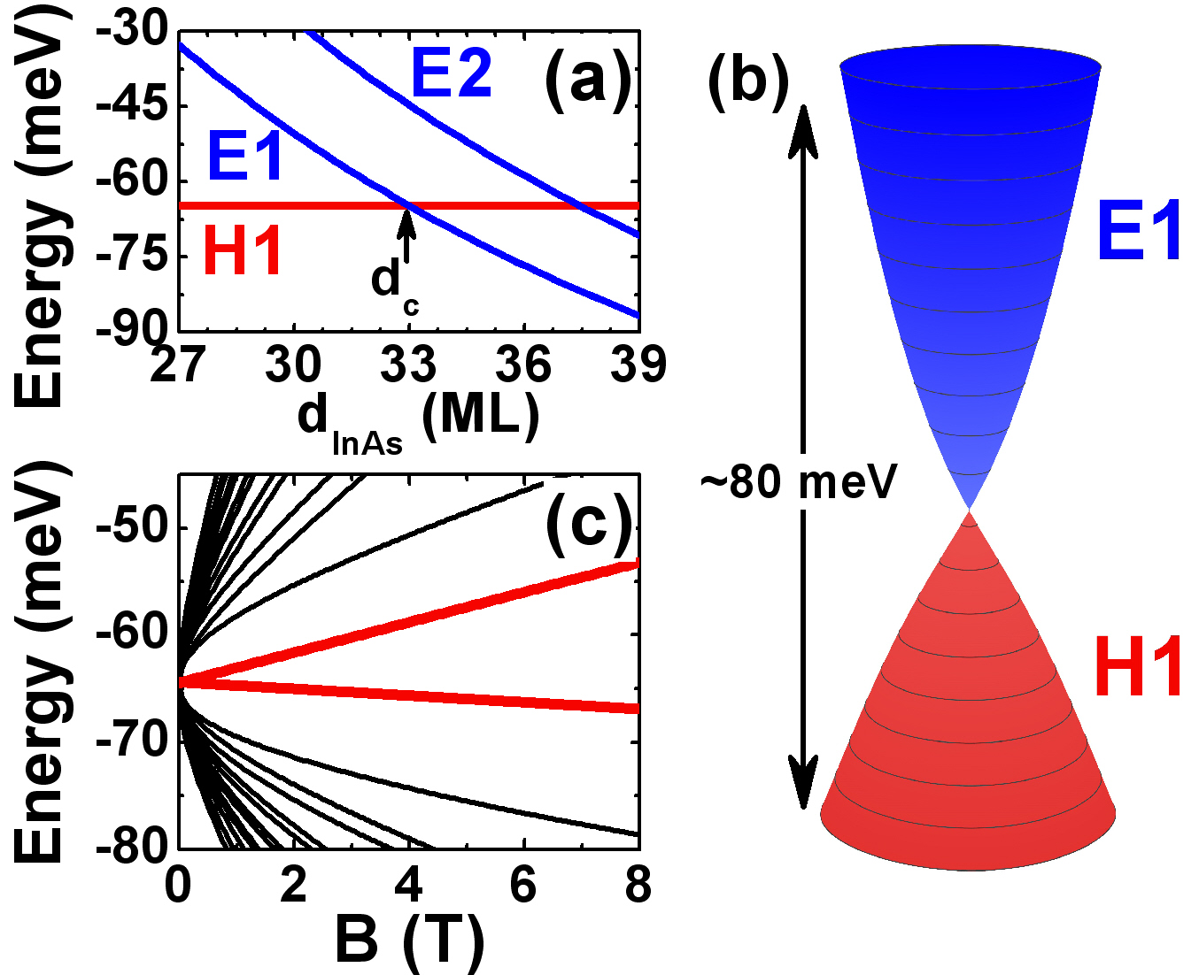
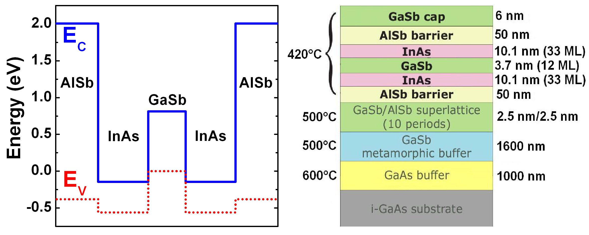
As mentioned above, the band structure of three-layer InAs/GaSb/InAs QWs, related to the mutual position of electron-like and hole-like subbands, strongly depends on the layer thicknesses Krishtopenko and Teppe (2018a). When the InAs and GaSb layers are both thin, the first electron-like (E1) and hole-like (H1) subbands correspond to the conduction and valence bands respectively and the QW has a trivial band ordering. For thicker layers, the E1 subband drops below the H1 subband, as shown in Fig. 1a, and the system has an inverted band ordering. In this case, the conduction and valence bands are represented by the hole-like and electron-like levels, respectively.
One can use a simplified Dirac-like Hamiltonian Bernevig et al. (2006) to describe the electronic states when the energy difference between E1 and H1 subbands is small. Within the representation defined by the basis E1,+, H1,+, E1,-, H1,-, it has the form:
where asterisk stands for complex conjugation, is the momentum in the QW plane, are the Pauli matrices, , , , and . The structure parameters , , , , depend on the layer thicknesses. The mass parameter is positive for trivial band ordering and negative for inverted band structure. If we only keep the terms up to linear order in for each spin, then and at correspond to massless Dirac Hamiltonians. We note that the latter is valid if the InAs/GaSb/InAs QW has an inversion symmetry in the growth direction Murakami et al. (2007). In this case, the E1 and H1 subbands cross at the point, and their energy dispersion calculated from an eight-band Kane model is found to linearly depend on the quasimomentum at small , as shown in Fig. 1b.
Besides the linear terms, also contains quadratic terms, which cannot be neglected even at the energies close to the band crossing point. Moreover, they result in relevant difference between conventional massless DFs in graphene Novoselov et al. (2005); Castro Neto et al. (2009); Novoselov et al. (2004); Beenakker (2008) and the ones in symmetric InAs/GaSb/InAs QWs (and in HgTe QWs Büttner et al. (2011); Zholudev et al. (2012); Ludwig et al. (2014) as well). LLs in graphene are characterized by both a square-root dependence of their energies on the magnetic field and presence of so-called zero-energy LLs independent of the field. Note that all LLs in graphene have a spin-degeneracy (for simplicity, we consider the electrons in one valley and neglect the small Zeeman effect). This case is described by the linear terms in and at SM .
The parabolic terms remove the spin degeneracy of all LLs SM and, particularly, transform the spin-degenerate zero-energy LL into a pair of spin-polarized zero-mode LLs König et al. (2007), as shown in Fig. 1c. The electron-like zero-mode LL splits from the edge of the E1 subband and tends toward high energy with increasing magnetic field. In contrast, the second level, which decreases with magnetic field, has a hole-like character and arises from the H1 subband. Therefore, the crossing of the zero-mode LLs at finite value of magnetic field occurs in the inverted region, and is absent for Kadykov et al. (2018). A crossing of the zero-mode LLs at zero magnetic field gives a direct indication for the massless DFs in the QW.
The sample studied in this work was grown by molecular beam epitaxy (MBE) on a semi-insulating (001) GaAs substrate with a relaxed GaSb buffer. In order to get the gapless state, the thicknesses of InAs and GaSb layers were 33 ML and 14 ML, respectively (see Fig. 1). After the growth, a 50 m wide gated Hall bar was fabricated by using a single-mesa process. All details are provided in the Supplemental Materials SM .
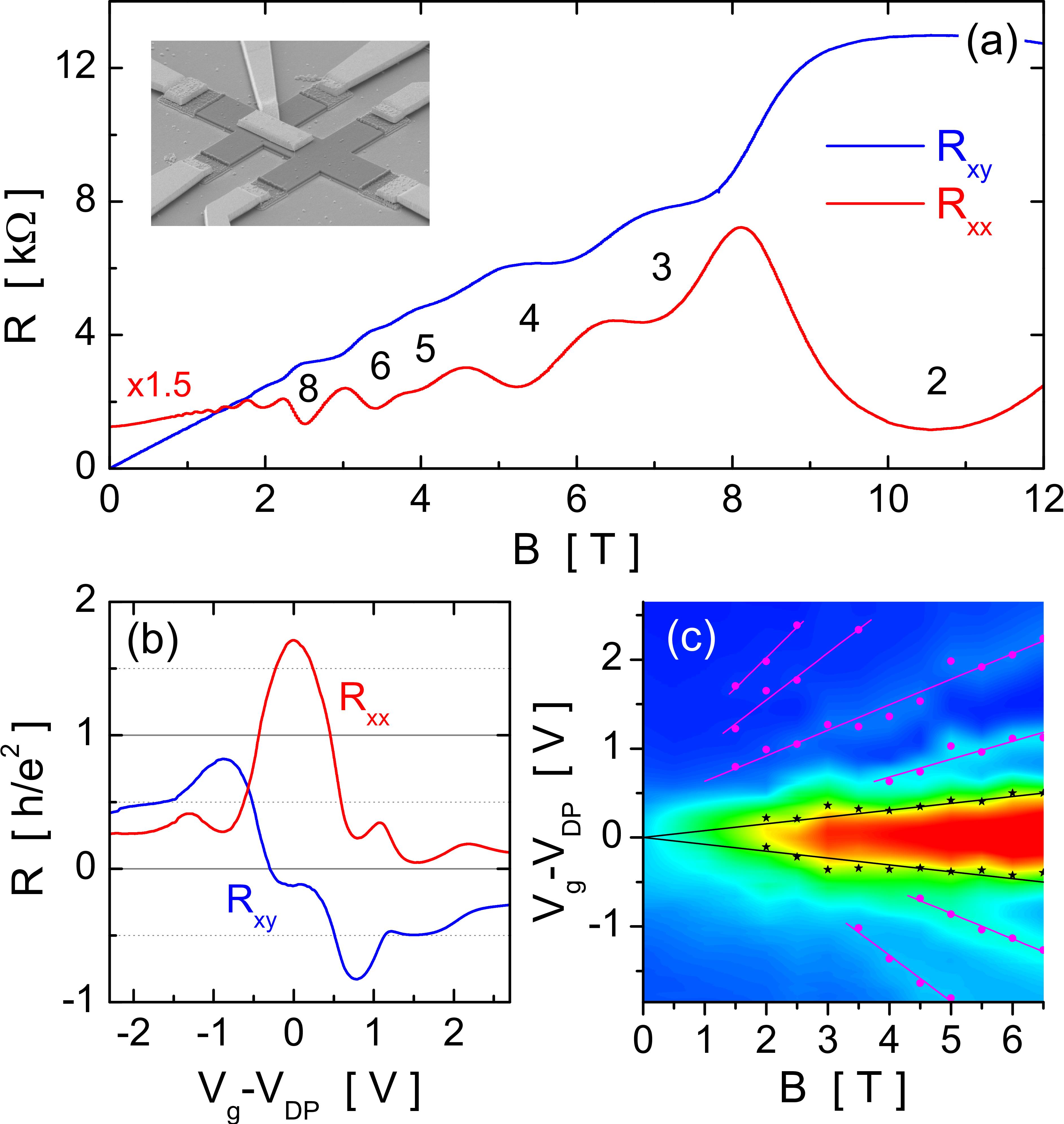
First, we investigate magnetotransport in our sample. Figure 2a presents the magnetic field dependence of the longitudinal and Hall resistances at K. The Hall density extracted from the measurements is equal to cm-2 with electron carriers at zero gate voltage and a mobility of cm2V-1s-1. The Hall resistance shows well-defined plateaus as a function of magnetic field at both even and odd multiples of associated to minima in the Shubnikov-de Haas (ShdH) oscillations, proving a 2D character of charge carriers in our structure. To vary the carrier density in the QW, we apply a gate voltage to the top gate. Typical gate voltage dependencies of and at T are shown in Fig. 2b (the low-field data are provided in the Supplemental Materials SM ).
The longitudinal resistance shows clear oscillations on each side as a function of of the central peak occurring at V when the Hall resistance presents plateaus and a sign reversal. These features demonstrate a changing of carrier concentration at different and the inversion of the type of carriers from electrons to holes at large negative gate voltage. Furthermore, an insulating behavior is observed at around with and small values of . The evolution of this insulating state is plotted in a 2D color map of as a function of and (Fig. 2c). It is evident that the size of the insulating region (red area) increases with . The linear extrapolation down to zero field of the points (black stars), corresponding to the position of the zero-mode LLs Büttner et al. (2011); Kadykov et al. (2018) and delimiting the high resistance region for T, demonstrates that the insulating state vanishes at T. This is also confirmed by the analysis of provided in the Supplemental Materials SM . Thus, the crossing of the zero-mode LLs at T indeed confirms the gapless state in our sample. The traces of higher LLs of electrons and holes are also seen for higher than V and lower than V, respectively.
The hallmark of 2D massless DFs is a specific sequence of quantum Hall plateaux observed at odd multiples of , where is valley degeneracy factor Castro Neto et al. (2009). In HgTe QWs (), the odd-integer quantum Hall sequence is much less pronounced Büttner et al. (2011) than in graphene Novoselov et al. (2005) () and observed at small (less than 1 T) magnetic fields only. The latter is caused by prominent contribution of the parabolic terms in , which remove the spin degeneracy of all LLs already at moderate fields as discussed above. In our sample, both odd and even plateaux are observed (see Fig. 2), and the quantum Hall effect looks like the one in conventional 2D electron gas Klitzing et al. (1980). This may be interpreted in two different ways.
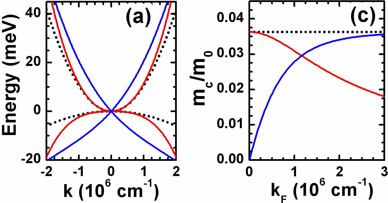
First, large contribution of terms proportional to and in results in significant spin splitting of LLs making impossible observation of the odd-integer sequence. Second, our sample may host the gapless state with parabolic band touching. As it is shown in the Supplemental Materials SM , band dispersion in for the latter case up to the third order has the form:
| (1) |
where ”” and ”” represent to the conduction and valence bands, respectively. Here, corresponds to the opposite parity of conduction and valence band, while for the same parity, one should set SM . Note that the linear dispersion is described by . The band dispersions at specific parameters are shown in Fig. 3a.
An efficient way to discriminate these two gapless states is the measurement of quasiclassical CR at different Fermi level positions. Applying a quasiclassical quantization rule to and , the cyclotron mass in the conduction band as a function of Fermi momentum has the forms
| (2) |
and
| (3) |
for the linear and parabolic case, respectively. As it is seen from Fig. 3b, the linear and parabolic gapless states have different behavior of cyclotron mass as a function of .
Figures 4a and 4b show CR spectra measured at K with both backward wave oscillator (BWO) at 845 GHz Aleshkin et al. (2005b); Kalinin et al. (2013) and quantum cascade laser (QCL) at 3 THz Ikonnikov et al. (2010) (pulse duration of 3 s; repetition period of 100–200 s) at different electron concentrations varied by using PPC effect SM . The measurements were performed on the unprocessed sample with a changing of the electron concentration by varying the time illumination from red and blue light emitting diodes placed close to the sample. The GHz/THz radiation passing through the sample was detected either by a silicon bolometer (for BWO) or Ge:Ga photoresistor (for QCL). The electron concentration was determined along with the CR measurements via magnetotransport measurements in the van der Pauw or two-terminal geometry.
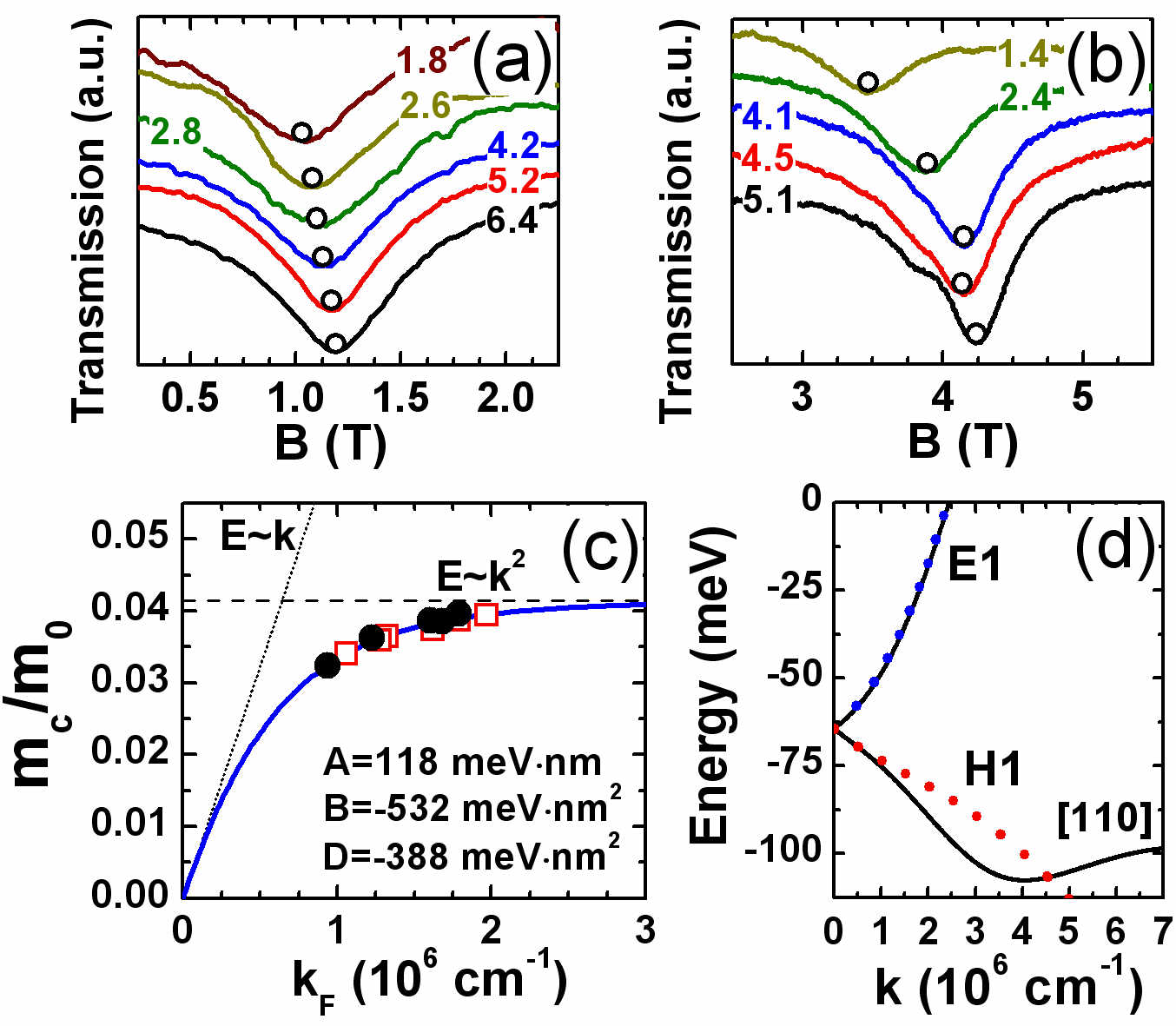
All the spectra contain a single CR line, defining the cyclotron mass at the Fermi level. As it is seen from Fig. 4a and 4b, CR lines shift toward high magnetic field with increasing of electron concentration. This indicates that cyclotron mass is strictly increasing function of , This fact excludes the gapless state with parabolic band touching in our sample. As it is discussed above, this mass dependence corresponds to the gapless state with the linear band crossing. In order to extract parameters of massless DFs, we have fitted our experimental data by Eq. (2). A good agreement with experimental values is achieved for meVnm, meVnm2 and meVnm2. Additionally, we plot the dependencies for (dotted curve) and (dashed curve) for pure linear and quadratic band dispersion, respectively.
Figure 4c shows that although there are indeed massless DFs with velocity m/s, they only exist in the immediate vicinity of the point at cm-2, while the terms proportional to and are relevant at higher concentrations. Note that additional measurements of temperature dependence of the conductivity at the charge neutrality point also evidences the massless DFs (see the Supplemental Materials SM ). Existence of pure massless DFs at small electron concentration is consistent with the absence of odd-sequence of quantum Hall plateaux in magnetotransport of our sample. For instance, for an odd Hall plateau with corresponding to LLs filling factor in linear dispersion regime, one should have well-resolved peaks of at magnetic field of 0.08 T. The latter cannot be achieved at the electron mobility of our sample.
Figure 4d compares band structure of the sample numerically calculated within the eight-band Kane model with the analytical expression for with the parameters extracted from the fitting . There is indeed a good agreement for the conduction band, while the valence band is well described at small quasimomentum only. This is also typical for HgTe/CdTe QWs Marcinkiewicz et al. (2017); Kadykov et al. (2018), in which the discrepancy for the valence band is explained by the effect of the remote subbands beyond the simplified Dirac-like Hamiltonian Krishtopenko and Teppe (2018b).
In conclusion, we have clearly observed massless DFs in III-V semiconductor QW. Magnetotransport experiments on a gated Hall bar allow us to demonstrate the absence of a band gap in our structure. The measurements of CR at different concentrations allow us not only determing the velocity m/s of the massless DFs, but also demonstrating significant effect of non-linear dispersion at high energies. Experimental dispersion of the massless DFs is in good agreement with realistic band structure calculations based on the eight-band Kane Hamiltonian.
Acknowledgements.
This work was supported by MIPS department of Montpellier University through the ”Occitanie Terahertz Platform”, by the Languedoc-Roussillon region via the ”Gepeto Terahertz platform” and the ARPE project ”Terasens” and by the CNRS through ”Emergence project 2016” and LIA ”TeraMIR”. MBE growth of the samples were performed within the French program ”Investments for the Future” (ANR-11-EQPX-0016). CR measurements were performed in the framework of Project 17-72-10158 provided by the Russian Science Foundation. S. S. Krishtopenko also acknowledges the Ministry of Education and Science of the Russian Federation (MK-1136.2017.2).References
- Novoselov et al. (2005) K. S. Novoselov, A. K. Geim, S. V. Morozov, D. Jiang, M. I. Katsnelson, I. V. Grigorieva, S. V. Dubonos, and A. A. Firsov, Nature 438, 197 (2005).
- Wehling et al. (2014) T. O. Wehling, A. M. Black-Schaffer, and A. V. Balatsky, Adv. Phys. 63, 1 (2014).
- Castro Neto et al. (2009) A. H. Castro Neto, F. Guinea, N. M. R. Peres, K. S. Novoselov, and A. K. Geim, Rev. Mod. Phys. 81, 109 (2009).
- Beenakker (2008) C. W. J. Beenakker, Rev. Mod. Phys. 80, 1337 (2008).
- Liang et al. (2015) T. Liang, Q. Gibson, M. N. Ali, M. Liu, R. J. Cava, and N. P. Ong, Nat. Mater. 14, 280 284 (2015).
- Novoselov et al. (2004) K. S. Novoselov, A. K. Geim, S. V. Morozov, D. Jiang, Y. Zhang, S. V. Dubonos, I. V. Grigorieva, and A. A. Firsov, Science 306, 666 (2004).
- Gerchikov and Subashiev (1990) L. G. Gerchikov and A. V. Subashiev, Phys. Status Solidi B 160, 443 (1990).
- Bernevig et al. (2006) B. A. Bernevig, T. L. Hughes, and S.-C. Zhang, Science 314, 1757 (2006).
- Büttner et al. (2011) B. Büttner, C. Liu, G. Tkachov, E. Novik, C. Brüne, H. Buhmann, E. Hankiewicz, P. Recher, B. Trauzettel, S. Zhang, and L. Molenkamp, Nat. Phys. 7, 418 (2011).
- Zholudev et al. (2012) M. Zholudev, F. Teppe, M. Orlita, C. Consejo, J. Torres, N. Dyakonova, M. Czapkiewicz, J. Wróbel, G. Grabecki, N. Mikhailov, S. Dvoretskii, A. Ikonnikov, K. Spirin, V. Aleshkin, V. Gavrilenko, and W. Knap, Phys. Rev. B 86, 205420 (2012).
- Ludwig et al. (2014) J. Ludwig, Y. B. Vasilyev, N. N. Mikhailov, J. M. Poumirol, Z. Jiang, O. Vafek, and D. Smirnov, Phys. Rev. B 89, 241406 (2014).
- Ikonnikov et al. (2016) A. V. Ikonnikov, S. S. Krishtopenko, O. Drachenko, M. Goiran, M. S. Zholudev, V. V. Platonov, Y. B. Kudasov, A. S. Korshunov, D. A. Maslov, I. V. Makarov, O. M. Surdin, A. V. Philippov, M. Marcinkiewicz, S. Ruffenach, F. Teppe, W. Knap, N. N. Mikhailov, S. A. Dvoretsky, and V. I. Gavrilenko, Phys. Rev. B 94, 155421 (2016).
- Kotov et al. (2012) V. N. Kotov, B. Uchoa, V. M. Pereira, F. Guinea, and A. H. Castro Neto, Rev. Mod. Phys. 84, 1067 (2012).
- Wiedmann et al. (2015) S. Wiedmann, A. Jost, C. Thienel, C. Brüne, P. Leubner, H. Buhmann, L. W. Molenkamp, J. C. Maan, and U. Zeitler, Phys. Rev. B 91, 205311 (2015).
- Krishtopenko et al. (2016a) S. S. Krishtopenko, I. Yahniuk, D. B. But, V. I. Gavrilenko, W. Knap, and F. Teppe, Phys. Rev. B 94, 245402 (2016a).
- Marcinkiewicz et al. (2017) M. Marcinkiewicz, S. Ruffenach, S. S. Krishtopenko, A. M. Kadykov, C. Consejo, D. B. But, W. Desrat, W. Knap, J. Torres, A. V. Ikonnikov, K. E. Spirin, S. V. Morozov, V. I. Gavrilenko, N. N. Mikhailov, S. A. Dvoretskii, and F. Teppe, Phys. Rev. B 96, 035405 (2017).
- Kadykov et al. (2018) A. M. Kadykov, S. S. Krishtopenko, B. Jouault, W. Desrat, W. Knap, S. Ruffenach, C. Consejo, J. Torres, S. V. Morozov, N. N. Mikhailov, S. A. Dvoretskii, and F. Teppe, Phys. Rev. Lett. 120, 086401 (2018).
- Teppe et al. (2016) F. Teppe, M. Marcinkiewicz, S. S. Krishtopenko, S. Ruffenach, C. Consejo, A. M. Kadykov, W. Desrat, D. But, W. Knap, J. Ludwig, S. Moon, D. Smirnov, M. Orlita, Z. Jiang, S. V. Morozov, V. Gavrilenko, N. N. Mikhailov, and S. A. Dvoretskii, Nat. Commun. 7, 12576 (2016).
- Miao et al. (2012) M. S. Miao, Q. Yan, C. G. Van de Walle, W. K. Lou, L. L. Li, and K. Chang, Phys. Rev. Lett. 109, 186803 (2012).
- Zhang et al. (2013) D. Zhang, W. Lou, M. Miao, S.-C. Zhang, and K. Chang, Phys. Rev. Lett. 111, 156402 (2013).
- Krishtopenko and Teppe (2018a) S. S. Krishtopenko and F. Teppe, Sci. Adv. 4, eaap7529 (2018a).
- Krishtopenko et al. (2018) S. S. Krishtopenko, S. Ruffenach, F. Gonzalez-Posada, G. Boissier, M. Marcinkiewicz, M. A. Fadeev, A. M. Kadykov, V. V. Rumyantsev, S. V. Morozov, V. I. Gavrilenko, C. Consejo, W. Desrat, B. Jouault, W. Knap, E. Tournié, and F. Teppe, Phys. Rev. B 97, 245419 (2018).
- Pikulin and Hyart (2014) D. I. Pikulin and T. Hyart, Phys. Rev. Lett. 112, 176403 (2014).
- Budich et al. (2014) J. C. Budich, B. Trauzettel, and P. Michetti, Phys. Rev. Lett. 112, 146405 (2014).
- Du et al. (2017) L. Du, X. Li, W. Lou, G. Sullivan, K. Chang, J. Kono, and R.-R. Du, Nat. Commun. 8, 1971 (2017).
- Xue and MacDonald (2018) F. Xue and A. H. MacDonald, Phys. Rev. Lett. 120, 186802 (2018).
- Gauer et al. (1993) C. Gauer, J. Scriba, A. Wixforth, J. P. Kotthaus, C. Nguyen, G. Tuttle, J. H. English, and H. Kroemer, Semicond. Sci. Technol. 8, S137 (1993).
- Sadofyev et al. (2005) Y. G. Sadofyev, A. Ramamoorthy, J. P. Bird, S. R. Johnson, and Y.-H. Zhang, Appl. Phys. Lett. 86, 192109 (2005).
- Aleshkin et al. (2005a) V. Y. Aleshkin, V. I. Gavrilenko, D. M. Gaponova, A. V. Ikonnikov, K. V. Maremyanin, S. V. Morozov, Y. G. Sadofyev, S. R. Johnson, and Y. H. Zhang, Semiconductors 39, 22 (2005a).
- Gavrilenko et al. (2010) V. I. Gavrilenko, A. V. Ikonnikov, S. S. Krishtopenko, A. A. Lastovkin, K. V. Maremyanin, Y. G. Sadofyev, and K. E. Spirin, Semiconductors 44, 616 (2010).
- Spirin et al. (2012) K. E. Spirin, K. P. Kalinin, S. S. Krishtopenko, K. V. Maremyanin, V. I. Gavrilenko, and Y. G. Sadofyev, Semiconductors 46, 1396 (2012).
- Tong et al. (2017) B. Tong, Z. Han, T. Li, C. Zhang, G. Sullivan, and R.-R. Du, AIP Advances 7, 075211 (2017).
- Ruffenach et al. (2017) S. Ruffenach, S. S. Krishtopenko, L. S. Bovkun, A. V. Ikonnikov, M. Marcinkiewicz, C. Consejo, M. Potemski, B. Piot, M. Orlita, B. R. Semyagin, M. A. Putyato, E. A. Emelyanov, V. V. Preobrazhenskii, W. Knap, F. Gonzalez-Posada, G. Boissier, E. Tournié, F. Teppe, and V. I. Gavrilenko, JETP Lett. 106, 727 (2017).
- Knebl et al. (2018) G. Knebl, P. Pfeffer, S. Schmid, M. Kamp, G. Bastard, E. Batke, L. Worschech, F. Hartmann, and S. Höfling, Phys. Rev. B 98, 041301 (2018).
- Murakami et al. (2007) S. Murakami, S. Iso, Y. Avishai, M. Onoda, and N. Nagaosa, Phys. Rev. B 76, 205304 (2007).
- (36) See Supplemental Materials, which also contain Refs. [43–51], for a brief discussion of simplified Dirac-like model in magnetic fields and details of magnetotransport measurements. The spectral studies of persistent photoconductivity of our sample are also provided therein .
- König et al. (2007) M. König, S. Wiedmann, C. Brüne, A. Roth, H. Buhmann, L. W. Molenkamp, X.-L. Qi, and S.-C. Zhang, Science 318, 766 (2007).
- Klitzing et al. (1980) K. v. Klitzing, G. Dorda, and M. Pepper, Phys. Rev. Lett. 45, 494 (1980).
- Aleshkin et al. (2005b) V. Y. Aleshkin, V. I. Gavrilenko, A. V. Ikonnikov, Y. G. Sadofyev, J. P. Bird, S. R. Johnson, and Y. H. Zhang, Semiconductors 39, 62 (2005b).
- Kalinin et al. (2013) K. P. Kalinin, S. S. Krishtopenko, K. V. Maremyanin, K. E. Spirin, V. I. Gavrilenko, A. A. Biryukov, N. V. Baidus, and B. N. Zvonkov, Semiconductors 47, 1485 (2013).
- Ikonnikov et al. (2010) A. V. Ikonnikov, A. V. Antonov, A. A. Lastovkin, V. I. Gavrilenko, Y. G. Sadof’ev, and N. Samal, Semiconductors 44, 1467 (2010).
- Krishtopenko and Teppe (2018b) S. S. Krishtopenko and F. Teppe, Phys. Rev. B 97, 165408 (2018b).
- Semenikhin et al. (2007) I. Semenikhin, A. Zakharova, K. Nilsson, and K. A. Chao, Phys. Rev. B 76, 035335 (2007).
- Semenikhin et al. (2008) I. Semenikhin, A. Zakharova, and K. A. Chao, Phys. Rev. B 77, 113307 (2008).
- Charpentier et al. (2013) C. Charpentier, S. Fält, C. Reichl, F. Nichele, A. N. Pal, P. Pietsch, T. Ihn, K. Ensslin, and W. Wegscheider, Appl. Phys. Lett. 103, 112102 (2013).
- Bolotin et al. (2008) K. Bolotin, K. Sikes, Z. Jiang, M. Klima, G. Fudenberg, J. Hone, P. Kim, and H. Stormer, Solid State Commun. 146, 351 (2008).
- Gusev et al. (2017) G. M. Gusev, D. A. Kozlov, A. D. Levin, Z. D. Kvon, N. N. Mikhailov, and S. A. Dvoretsky, Phys. Rev. B 96, 045304 (2017).
- Krishtopenko et al. (2016b) S. S. Krishtopenko, W. Knap, and F. Teppe, Sci. Rep. 6, 30755 (2016b).
- Rothe et al. (2010) D. G. Rothe, R. W. Reinthaler, C.-X. Liu, L. W. Molenkamp, S.-C. Zhang, and E. M. Hankiewicz, New J. Phys. 12, 065012 (2010).
- Tuttle et al. (1989) G. Tuttle, H. Kroemer, and J. H. English, J. Appl. Phys. 65, 5239 (1989).
- Tuttle et al. (1990) G. Tuttle, H. Kroemer, and J. H. English, J. Appl. Phys. 67, 3032 (1990).
Supplemental Materials
.1 A. Simplified Dirac-like 2D Hamiltonian
To describe qualitatively electronic states in QWs with inversion symmetry, one can use a simplified Dirac-like Hamiltonian Bernevig et al. (2006), proposed for the electronic states in E1 and H1 subbands in the vicinity of the point of the Brillouin zone. We note that the given subband is called as an electron-like E1 subband, if its electronic states at the point of the Brillouin zone are formed by a linear combination of the , and bulk bands, while the states in the hole-like H1 subband at have only contribution from the heavy-hole band Krishtopenko et al. (2016a, 2018). Using the basis states , , , , the Hamiltonian for the E1 and H1 subbands is written as
| (1) |
where
| (2) |
and
Here, are the momentum components in the QW plane, and , , and are specific QW constants, being defined by the QW geometry and material parameters. The two components of the Pauli matrices denote the E1 and H1 subbands, whereas the two diagonal blocks and represent spin-up and spin-down states, which are linked together by time-reversal symmetry. Here, as in the main text, we have neglected the terms, arising due to the bulk inversion asymmetry (BIA) of the unit cell Semenikhin et al. (2007) and the interface inversion asymmetry (IIA) Semenikhin et al. (2008). The most important quantity in is the mass parameter , which describes the ordering of E1 and H1 subbands. At the critical temperature , the mass parameter is equal to zero. If we then only keep the linear terms in k for each spin, and correspond to Hamiltonians, describing massless Dirac fermions. As it has no valley degeneracy, the QW with offers realization of single-valley massless Dirac fermions with the velocity defined by the parameter .
To calculate Landau levels (LLs) in the presence of an external magnetic field oriented perpendicular to the QW plane, one should make the Peierls substitution, , where in the Landau gauge . Additionally, we add the Zeeman term in the Hamiltonian
| (3) |
where is the Bohr magneton, and are the effective (out-of-plane) g-factors of the E1 and H1 subbands, respectively.
Solving the eigenvalue problem for the upper block of , the LL energies are found analytically König et al. (2007):
| (4) |
For the lower block of , the LL energies are written as
| (5) |
Here is the magnetic length given by . The LLs with energies and are called the zero-mode LLs König et al. (2007). They split from the edge of E1 and H1 subbands and tend toward conduction and valence band as a function of , respectively.
If we put to zero and omit quadratic terms in the Hamiltonian , Eqs. (4,5) are rewritten as
| (6) |
Omitting the Zeeman terms proportional to and , we arrive at the spin-degenerate spectrum for LLs in graphene Castro Neto et al. (2009) with a square-root dependence of their energies on .
.2 B. The sample fabrication
Figure S1 schematically shows the band-edge diagram and the growth scheme for three-layer InAs/GaSb/InAs QWs sandwiched between AlSb barriers. The QW studied in this work was grown by solid-source molecular beam epitaxy on a semi-insulating (001) GaAs substrate. After deoxidation at around 600 ∘C a thick undoped GaAs buffer layer was grown. The large lattice-mismatch between GaAs, GaSb and AlSb (8%) was accommodated through a thick GaSb buffer layer of 1.6 m followed by a ten-period 2.5 nm GaSb/2.5 nm AlSb superlattice (SLS), all grown at 500 ∘C. Subsequently, the substrate temperature was decreased down to 420 ∘C to grow the three-layer InAs/GaSb/InAs QW confined by 50-nm thick AlSb barrier layers. A 6-nm GaSb cap layer was used to prevent oxidation of the AlSb barrier layers (see Fig. S1b). The shutter sequences at all InAs/GaSb interfaces were organized in order to promote the formation of InSb-like interfaces, which gives higher electron mobilities (in contrast to AlAs-like interfaces) Tuttle et al. (1990). The barriers on both sides of the QW were nominally undoped. To have a gapless state in the QW, the thicknesses of the InAs and GaSb layers were adjusted to 33 ML and 14 ML, respectively (see Fig. 1 in the main text), where 1 ML corresponds to half of the lattice constant of the bulk material.
The gated Hall bars were fabricated by using a single-mesa process. The fabrication process was defined by standard electron-beam lithography allowing a large scale of size defined between 400 nm and 50 m. The process started by the ohmic contact lithography level definition followed by a Pd-based metallization performed by e-beam evaporation. The ohmic contact metallization is then annealed at 300∘C using a rapid thermal annealing (RTA). Then, 200 nm of SiO2 was deposited by plasma enhanced chemical vapour deposition at 200∘C. This layer is used as dielectric and allows the fabrication of a gated MOS structure for controlling the carrier density in the QW. The gate lithography was then defined followed by a Ti-based metal gate evaporation. The next step consists in the etching of the SiO2 layer using the gate as a mask. The SiO2 layer is only removed around the Hall bar, the remaining SiO2 being used to isolate the pads from the conductive substrate. To complete the Hall bar, the mesa isolation is done by dry etching using the ohmic contact, gate metal and the SiO2 as a hard mask. Finally, the ohmic contacts and the gate are connected to the pads using air bridges.
.3 C. Details of magnetotransport measurements
Magnetotransport measurements have been performed on 50 m wide Hall bars with a low frequency 100 nA ac current. Samples are placed in a variable temperature insert equipped with a T superconducting coil. Cooling the Hall bars from room temperature down to K reveals a weak insulating behavior as the resistivity doubles. At low temperature the quantum lifetime of the carriers is evaluated from the Shubnikov-de Haas oscillations at low magnetic field and is found equal to ps. The transport scattering time obtained from the mobility is ps, i.e. only 2 times larger than . An estimate of the LL broadening gives meV at zero gate voltage.
Figure S2 plots , i.e. the electron and hole concentration in a one-carrier approximation at T, as a function of gate voltage . The carrier density decreases linearly with changing of from positive to negative values. At the Dirac point V, the data shows an unequivocal inversion of the carrier type versus gate voltage in the QW.
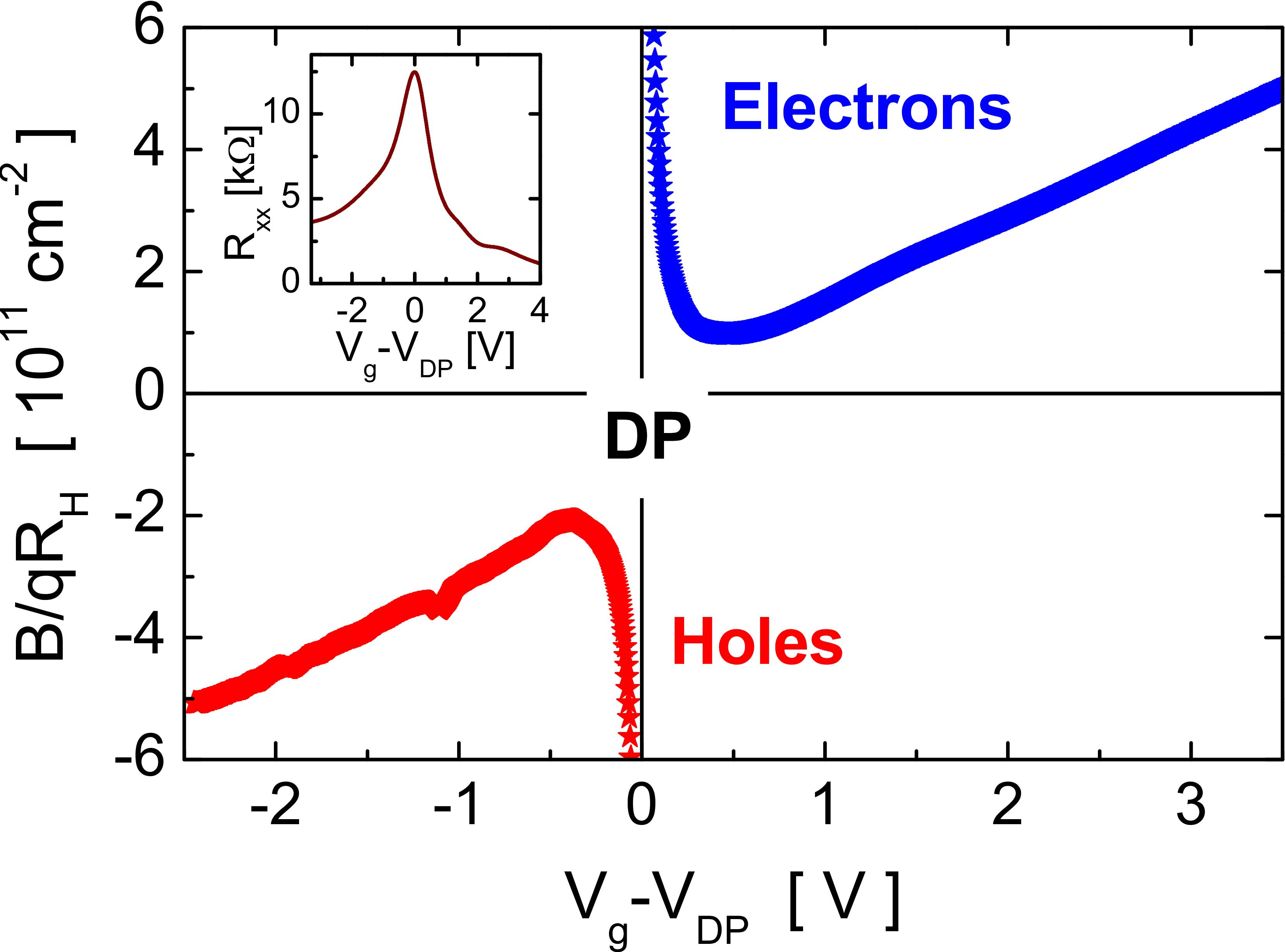
The continuous transition from electrons to holes evidences a gapless state of the QW. At the same time, the longitudinal resistance becomes maximum, when the Fermi level crosses the Dirac point (see the inset in Fig. S2). The carrier density variation with gate voltage is similar for electrons and holes with cm-2/V and cm-2/V. It means that the conduction and valence band dispersions are almost symmetric in the vicinity of the point of the Brillouin zone.
Next, we assume that the carrier density dependence on the gate voltage is controlled mainly by the geometric capacitance of the structure, i.e. . By considering a parallel plate capacitor composed of the silicon oxide layer ( nm), the GaSb cap layer ( nm) and the AlSb barrier ( nm), the equivalent capacitance equals F/cm2. It leads to a filling rate of cm-2/V which is in agreement with the experimental one. The discrepancy can be explained by the presence of additional charges in the oxide. Indeed a slow drift of the carrier density occurs as the gate is maintained at a fixed negative bias. This effect is minimized during the measurement by scanning the gate voltage back and forth.
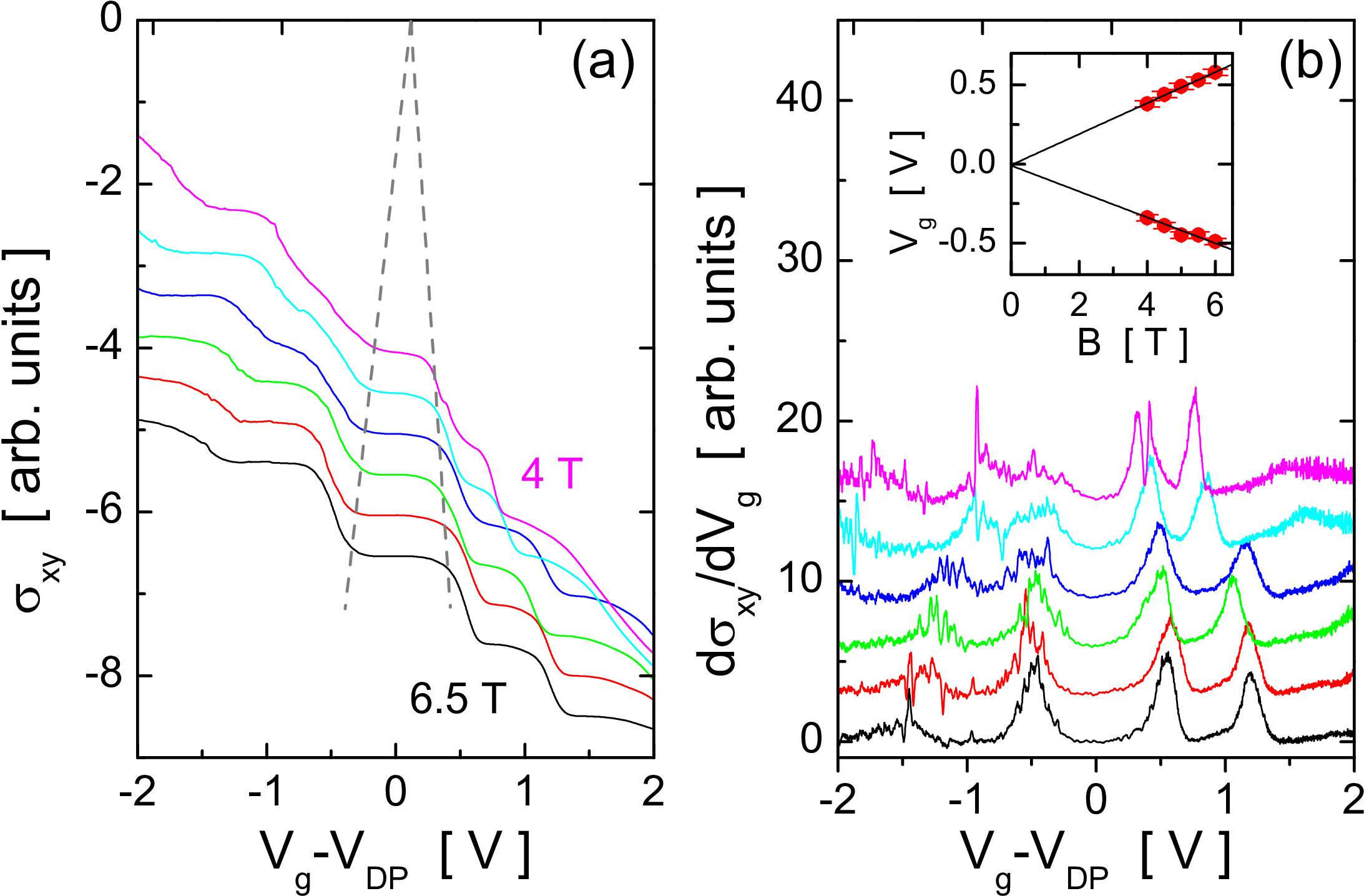
Figure S3a shows the transverse conductivity as a function of gate voltage for different magnetic fields. The width of the plateau at zero bias shrinks clearly when diminishes and tends to zero when T. We underline that only conductivity traces obtained at sufficiently high magnetic fields are plotted for clarity. The plateau is strongly smoothed at lower fields. A reliable method for extracting the critical field correctly is to plot the maxima in the curves as a function of (see Fig. S3b and its inset). The linear extrapolation indicates that the gap cancels out at T, which confirms the critical field value measured from the criterion reported in the main text.
.4 D. Temperature dependence of conductivity at charge neutrality point
Figure S4a plots the resistance versus swing voltage at different temperatures measured on a second Hall bar. The graph clearly shows the peaked resistivity behavior expected for Dirac-like 2D systems Büttner et al. (2011); Bolotin et al. (2008); Gusev et al. (2017). As can be seen, the maximum of decreases with . Figure S4b shows the conductivity at the Dirac point as a function of temperature. Qualitatively, the temperature dependence of is written as Büttner et al. (2011):
| (7) |
| (8) |
where is the spectral broadening induced by spin-independent potential disorder and is the variance of the gap due to spatial deviations of the layer thicknesses from their critical values.
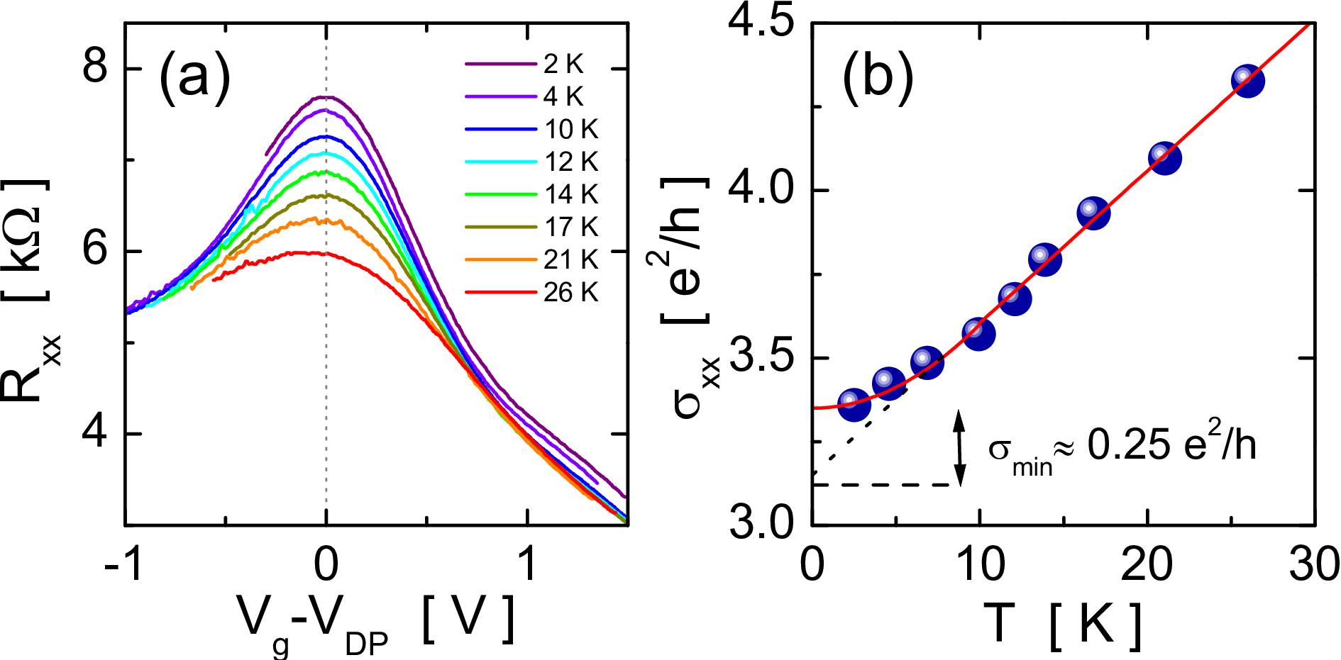
As seen from Fig. S4b, the conductivity shows a quadratic dependence on at low temperature with the minimal value . This large value is caused by partial conduction via the sample bulk, which is typical for the InAs/GaSb QWs Charpentier et al. (2013). In order to estimate the residual conductivity, the linear dependence of at high temperature is extrapolated down to K. By subtracting the obtained value to we find . As clear from Eq. (8), the conductivity slope at high is inversely proportional to the broadening parameter induced by the disorder. By fitting the high-temperature values, we obtain meV, which is in a good agreement with the LL broadening of meV extracted from magnetotransport (see Fig. 2 in the main text and Sec. C). From the values of and , we also evaluate the gap fluctuation in our sample meV. We note that the linear temperature dependence of at high resulting from the linear density of states is another manifestation of the DFs in the QW Büttner et al. (2011).
.5 E. Quadratic band touching in zinc-blende QWs
Let us now consider various cases of quadratic band touching at the point of Brillouin zone, which may exist in symmetric zinc-blende QWs grown in the [001] direction. The form of effective Hamiltonian for quadratic band touching can be obtained from the symmetry considerations. For simplicity, we neglect the terms, arising due to the bulk inversion asymmetry (BIA) of the unit cell Semenikhin et al. (2007) and the interface inversion asymmetry (IIA) Semenikhin et al. (2008).
In this case, for electronic QW states at the point with in-plane momentum , we have three types of symmetries: the time reversal symmetry, the inversion symmetry and the in-plane full rotation symmetry Krishtopenko et al. (2016b); Krishtopenko and Teppe (2018); Rothe et al. (2010). Time reversal symmetry relates states with opposite spin to each other; hence when the effective Hamiltonian for one spin is constructed, the Hamiltonian for the opposite spin can be easily obtained through the time-reversal operation. The inversion operation defines the parity of each subband, while in-plane rotation symmetry allows for conservation of the total angular momentum along the growth QW direction. Both inversion and in-plane full rotation symmetries define the form of matrix elements in the effective Hamiltonian. From the symmetry considerations mentioned above, the general form of the effective Hamiltonian describing quadratic band touching is
| (9) |
where has the form similar to in Eq. (2):
| (10) |
As we intend to keep in only the terms up to the third order in , and can be written as
| (11) |
where
First, we consider the case of different parity of the conduction and valence band. Away from the point, these states can mix. However, the coupling matrix element between these two states must be an odd function of the in-plane momentum and obey full rotation symmetry. Thus, we deduce two forms of in :
| (12) |
The former can be realized in 2D system, described by in the absence of linear term Rothe et al. (2010), while the latter takes place in double HgTe QWs Krishtopenko et al. (2016b) or GaSb/InAs/GaSb QWs Krishtopenko and Teppe (2018). The energy dispersion for these two cases has the same form:
| (13) |
where ”” and ”” correspond to the conduction and valence bands, respectively.
In the opposite case of the same parity of conduction and valence band, the coupling matrix element must be an even function of . Taking into account the full rotation symmetry, the non-zero is written as:
| (14) |
resulting to the following band dispersion:
| (15) |
As it is seen that in terms of band dispersion, the interband mixing formally results in renormalization of , which is now written as .
.6 F. Persistent photoconductivity effect
Persistent photoconductivity (PPC) is the phenomenon of long-term modification of the material conductivity after the action of light at low temperatures. If the sample conductivity increases after illumination, the effect is called positive PPC. In the case of conductivity decreasing after the action of light, PPC is named as negative. The inherent property of the InAs-based QWs is the bipolarity of PPC, arising under illumination of the sample at different wavelengths Tuttle et al. (1989); Gauer et al. (1993); Aleshkin et al. (2005); Gavrilenko et al. (2010); Tong et al. (2017); Knebl et al. (2018). The negative PPC was first observed in Tuttle et al. (1989) under the illumination by green light emitting diode (LED), while the positive PPC was measured in Gauer et al. (1993) under the influence of infrared (IR) light. By using bipolar PPC, the electron concentration can be reversibly changed by several times, which offers tuning the Fermi level in the sample without a gate.
As we are interested in the states close in energy to the band crossing point (see the main text), we first determine the wavelength of the LED, providing the most efficient way to decrease the electron concentration in our sample. For such purpose, we perform a spectral study of PPC effect. The scheme of experimental setup is based on MDR-23 grating monochromator Aleshkin et al. (2005). A quartz incandescent lamp was used as the radiation source, and the higher-order diffraction peaks were cut off by standard filters. At the monochromator output, radiation with photon energy from 0.6 to 4 eV was coupled to an optical fiber and delivered to the sample holder in helium cryostat. In the PPC study, we used the rectangular samples of the Hall geometry with two strip indium ohmic contacts deposited at the edges. A dc current of 1 A was passed through the sample placed at the center of a superconducting solenoid. All the measurements were performed at K.
The photoconductivity spectra were recorded in two different modes. In the first mode the measurements were performed step by step starting from the long-wavelength part of the spectrum. The sample was illuminated with monochromatic radiation then after switching off the illumination, to restore the ”equilibrium” value of the resistance, the exposure was performed (typically a few tens of seconds) and magnetotransport measurements were carried out. Then the monochromator was re-tuned to a shorter wavelength and the procedure repeated. To determine the electron concentration, we also measured resistances as a function of magnetic field in a two-stripe geometry. In the second mode, the measurements were performed under continuous illumination of monochromatic radiation with the wavelength slowly scanned starting from the short-wavelength part of the spectrum. The scanning pitch on the wavelength was 2 nm in the short-wavelength part and 20 nm in the long-wavelength part of the spectrum. After each step the signal was averaged during time which in our measurements was typically 20 seconds. The typical time of a spectral recording was several hours.
Figure S5a represents the PPC spectrum for our sample. For comparison, the inset also provides PPC spectra for the single InAs/AlSb QW of 15 nm width (B824) Aleshkin et al. (2005) and a 15 nm wide double InAs/AlSb QW with the middle AlSb barrier of 5 nm thickness (D003) Gavrilenko et al. (2010), both without GaSb layer in the QW. In the long-wavelength part of the spectrum at nm, the positive PPC is observed (the resistance is lower than the dark one). In the range between 300 and 1000 nm, a pronounced negative PPC is clearly seen. The measurements of maximum electron concentration achieved at the given wavelength (when the sample resistance saturates) show a clear correlation between spectral dependencies of the resistance and electron concentration (see Fig. S5b). In the spectral range of positive PPC an increase of electron concentration (compared to the dark value) is seen, while in the range of negative PPC the concentration decreases. Thus, PPC effect can be indeed used as an optical gating for the sample.
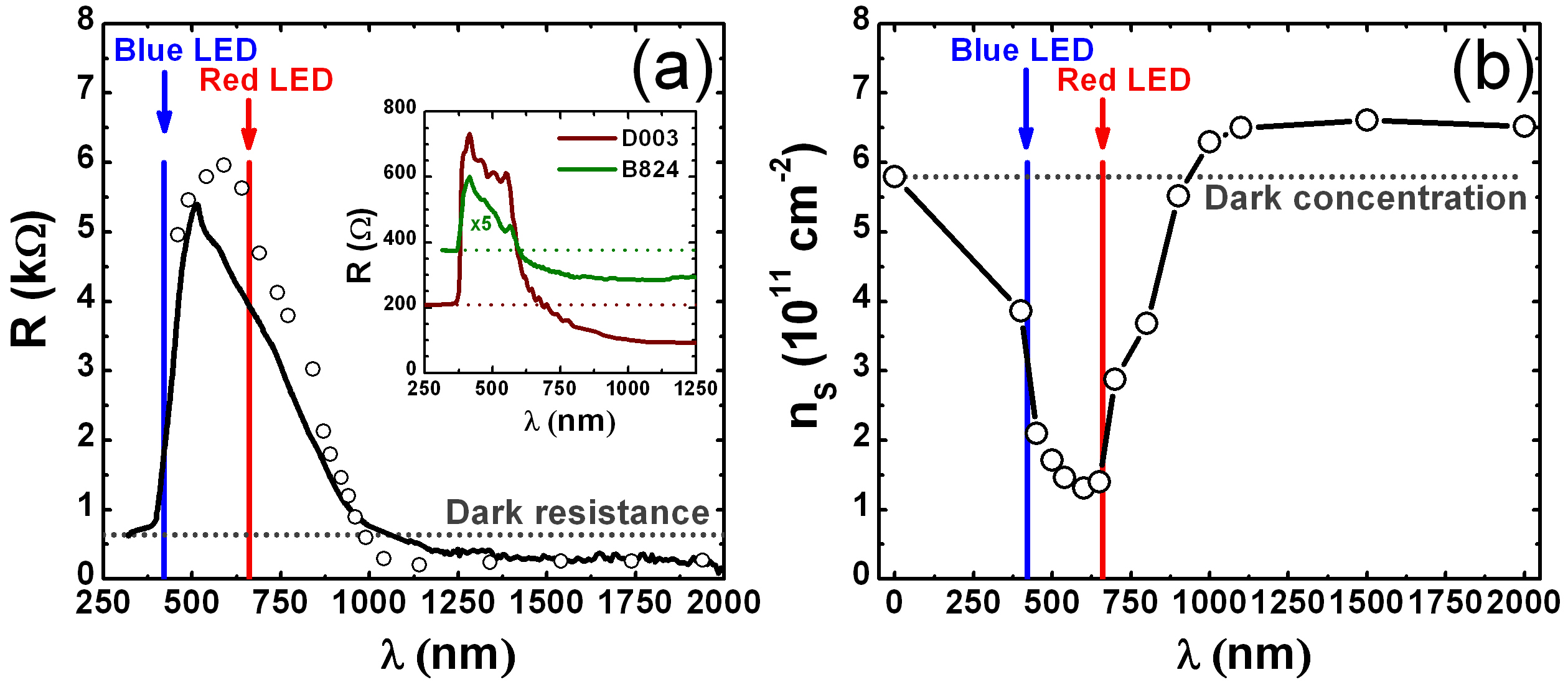
By comparing the PPC spectrum of our sample with the spectra of single and double InAs/AlSb QWs shown in the inset, we conclude that the main spectral features of PPC in all the cases coincide. It means that the origin of PPC in our sample and in InAs/AlSb QWs should be the same. The differences in the width of the negative PPC range are caused by the presence of the GaSb layer in the QWs. As it is recently shown for the InAs/Ga(In)Sb QW bilayers Tong et al. (2017), it affects a lot the QW response to the IR illumination.
Both positive and negative PPC are caused by recharge of the deep donors in the GaSb cap layer Gauer et al. (1993); Aleshkin et al. (2005); Gavrilenko et al. (2010). As it was shown in Gauer et al. (1993); Aleshkin et al. (2005), the negative PPC is mainly associated with the charge transfer from the InAs QW to the charged surface donors in the cap GaSb layer. The negative PPC is related with band gap excitation of electron-hole pairs firstly in the GaSb cap layer and then (at shorter wavelengths) in the AlSb barriers. Photoexcited electrons are captured by ionized deep donors, while the holes drift in the AlSb barriers in the ”built-in” electric field to the interface AlSb/InAs, where they recombine with electrons in InAs QW, thus, decreasing 2D electron concentration.
Since the positive and negative PPC are reversible (i.e. by sequentially illuminating the sample by visible and IR radiation we can reversibly vary the 2D electron concentration in the structure), then, both positive and negative PPC should be finally associated with recharge of the same deep centers. As shown in Gavrilenko et al. (2010), the transfer of the electric charge from the GaSb cap layer under the IR illumination has a ”diffusive” character and is apparently performed via the impurity states in the AlSb barrier. Since the electron effective mass is smaller than the hole effective mass, electrons ”diffuse” more rapidly. The holes providing an excess of positive charges in the cap layer under the band-to-band illumination in GaSb will be captured by neutral surface donors in this case Gavrilenko et al. (2010). Note that the infrared photon energy is high enough to ionize the deep donors in the AlSb barriers, which also contributes into positive PPC effect.
In the cyclotron resonance measurements, we used both blue and red LEDs. However, illumination by the red LED resulted in a wider range of concentration than with the blue LED.
References
- Bernevig et al. (2006) B. A. Bernevig, T. L. Hughes, and S.-C. Zhang, Science 314, 1757 (2006).
- Krishtopenko et al. (2016a) S. S. Krishtopenko, I. Yahniuk, D. B. But, V. I. Gavrilenko, W. Knap, and F. Teppe, Phys. Rev. B 94, 245402 (2016a).
- Krishtopenko et al. (2018) S. S. Krishtopenko, S. Ruffenach, F. Gonzalez-Posada, G. Boissier, M. Marcinkiewicz, M. A. Fadeev, A. M. Kadykov, V. V. Rumyantsev, S. V. Morozov, V. I. Gavrilenko, C. Consejo, W. Desrat, B. Jouault, W. Knap, E. Tournié, and F. Teppe, Phys. Rev. B 97, 245419 (2018).
- Semenikhin et al. (2007) I. Semenikhin, A. Zakharova, K. Nilsson, and K. A. Chao, Phys. Rev. B 76, 035335 (2007).
- Semenikhin et al. (2008) I. Semenikhin, A. Zakharova, and K. A. Chao, Phys. Rev. B 77, 113307 (2008).
- König et al. (2007) M. König, S. Wiedmann, C. Brüne, A. Roth, H. Buhmann, L. W. Molenkamp, X.-L. Qi, and S.-C. Zhang, Science 318, 766 (2007).
- Castro Neto et al. (2009) A. H. Castro Neto, F. Guinea, N. M. R. Peres, K. S. Novoselov, and A. K. Geim, Rev. Mod. Phys. 81, 109 (2009).
- Tuttle et al. (1990) G. Tuttle, H. Kroemer, and J. H. English, J. Appl. Phys. 67, 3032 (1990).
- Büttner et al. (2011) B. Büttner, C. Liu, G. Tkachov, E. Novik, C. Brüne, H. Buhmann, E. Hankiewicz, P. Recher, B. Trauzettel, S. Zhang, and L. Molenkamp, Nat. Phys. 7, 418 (2011).
- Bolotin et al. (2008) K. Bolotin, K. Sikes, Z. Jiang, M. Klima, G. Fudenberg, J. Hone, P. Kim, and H. Stormer, Solid State Commun. 146, 351 (2008).
- Gusev et al. (2017) G. M. Gusev, D. A. Kozlov, A. D. Levin, Z. D. Kvon, N. N. Mikhailov, and S. A. Dvoretsky, Phys. Rev. B 96, 045304 (2017).
- Charpentier et al. (2013) C. Charpentier, S. Fält, C. Reichl, F. Nichele, A. N. Pal, P. Pietsch, T. Ihn, K. Ensslin, and W. Wegscheider, Appl. Phys. Lett. 103, 112102 (2013).
- Krishtopenko et al. (2016b) S. S. Krishtopenko, W. Knap, and F. Teppe, Sci. Rep. 6, 30755 (2016b).
- Krishtopenko and Teppe (2018) S. S. Krishtopenko and F. Teppe, Sci. Adv. 4, eaap7529 (2018).
- Rothe et al. (2010) D. G. Rothe, R. W. Reinthaler, C.-X. Liu, L. W. Molenkamp, S.-C. Zhang, and E. M. Hankiewicz, New J. Phys. 12, 065012 (2010).
- Tuttle et al. (1989) G. Tuttle, H. Kroemer, and J. H. English, J. Appl. Phys. 65, 5239 (1989).
- Gauer et al. (1993) C. Gauer, J. Scriba, A. Wixforth, J. P. Kotthaus, C. Nguyen, G. Tuttle, J. H. English, and H. Kroemer, Semicond. Sci. Technol. 8, S137 (1993).
- Aleshkin et al. (2005) V. Y. Aleshkin, V. I. Gavrilenko, D. M. Gaponova, A. V. Ikonnikov, K. V. Maremyanin, S. V. Morozov, Y. G. Sadofyev, S. R. Johnson, and Y. H. Zhang, Semiconductors 39, 22 (2005).
- Gavrilenko et al. (2010) V. I. Gavrilenko, A. V. Ikonnikov, S. S. Krishtopenko, A. A. Lastovkin, K. V. Maremyanin, Y. G. Sadofyev, and K. E. Spirin, Semiconductors 44, 616 (2010).
- Tong et al. (2017) B. Tong, Z. Han, T. Li, C. Zhang, G. Sullivan, and R.-R. Du, AIP Advances 7, 075211 (2017).
- Knebl et al. (2018) G. Knebl, P. Pfeffer, S. Schmid, M. Kamp, G. Bastard, E. Batke, L. Worschech, F. Hartmann, and S. Höfling, Phys. Rev. B 98, 041301 (2018).