Multilayer ion trap with three-dimensional microwave circuitry for scalable quantum logic applications
Abstract
We present a multilayer surface-electrode ion trap with embedded 3D microwave circuitry for implementing entangling quantum logic gates. We discuss the electromagnetic full-wave simulation procedure that has led to the trap design and the characterization of the resulting microwave field-pattern using a single ion as a local field probe. The results agree with simulations within the uncertainty; compared to previous traps, this design reduces detrimental AC Zeeman shifts by three orders of magnitude. The design presented here can be viewed as an entangling gate component in a library for surface-electrode ion traps intended for quantum logic operations.
1 Introduction
Trapped ions are a promising platform to explore applications in quantum simulation and quantum computation cirac_quantum_1995 ; blatt_entangled_2008 ; georgescu_quantum_2014 ; bermudez_assessing_2017 . Towards the ultimate goal of a large-scale universal quantum machine solving specific problems with a quantum speed-up montanaro_quantum_2016 , milestones for first experimental implementations of quantum algorithms and quantum simulations have recently been achieved debnath_demonstration_2016 ; monz_realization_2016 ; zhang_observation_2017 ; jurcevic_direct_2017 . However, in order to improve their practical use in substantial problems, the number of stored and manipulated qubits as well as the fidelity of operations have yet to be increased significantly, highlighting the remaining key ingredient of a scalable architecture monroe_scaling_2013 .
Surface-electrode traps seidelin_microfabricated_2006 , where all electrodes are located in a plane, represent a suitable scalable platform as they allow to implement elements of the so-called ’quantum CCD’ architecture wineland_experimental_1998 ; kielpinski_architecture_2002 . Based on well-developed microfabrication techniques, surface traps unite an intrinsically scalable fabrication with a high degree of reproducibility. In such a planar geometry, the ion is trapped and influenced by the potentials that are applied to the metal electrodes located at the very top of the structure. Scaling to large arrays of ion traps amini_toward_2010 will lead to complex electrode arrangements and thus make it indispensable to incorporate interconnections to lower layers embedded into the structure craik_microwave_2014 ; guise_ball-grid_2015 ; maunz_high_2016 . Any such layers would be shielded from the ion by the top metal layer, but can be used to supply the electrodes in the top layer with control voltages.
For universal qubit manipulation, single- and multi-qubit gates driven by microwave radiation ospelkaus_trapped-ion_2008 ; mintert_ion-trap_2001 benefit from microfabricated traps as the control elements can be included as an integrated microwave conductor in the trap design. For qubits with transition frequencies in the RF or microwave regime, such as in 9Be+, this enables direct access to the qubit transition and, for these atoms, thus avoids the necessity for a complex Raman laser system to carry out gates gaebler_high-fidelity_2016 ; ballance_high-fidelity_2016 . In contrast to laser-based schemes, achievable fidelities of the microwave approaches johanning_individual_2009 ; harty_high-fidelity_2016 ; ospelkaus_microwave_2011 ; khromova_designer_2012 ; weidt_trapped-ion_2016 show no fundamental limit due to photon scattering ozeri_errors_2007 and are approaching the fault-tolerant regime for universal gate sequences harty_high-fidelity_2014 ; harty_high-fidelity_2016 .
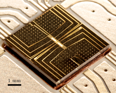
In this paper we introduce a microfabricated radio-frequency ion trap with integrated 3D microwave circuitry. Besides two microwave conductors that can be used to drive single-qubit gates, the trap design features an embedded 3D microwave conductor with a meander-like shape that has been designed to carry out multi-qubit gates using microwave near-fields. The trap has been produced in a novel multilayer fabrication process enabling a scalable trap architecture based on microwave (near-field) quantum logic bautista-salvador_multilayer_2019 .
In the following Sec. 2 we briefly introduce the fabrication process, trap design and experimental setup. Sec. 3 treats the design of the 3D microwave conductor usable for multi-qubit gates in more detail and highlights its advantages in terms of scalability and field properties when compared to a corresponding single-layer trap. In addition, we give a description of the full-wave simulation model used for extracting its resulting magnetic field configuration. In Sec. 4 we compare these simulations to experimental results, including an S-parameter measurement and a Ramsey-type, single-ion experiment to map out the produced field configuration. Finally, in Sec. 5 we summarize and conclude our findings.
2 Trap design and fabrication
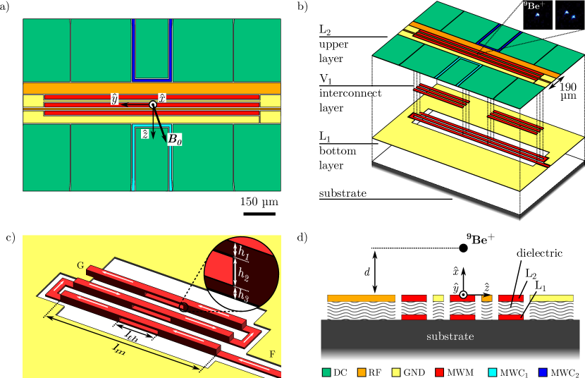
The trap presented here is a multilayer extension of a surface-electrode ion trap with integrated microwave conductors wahnschaffe_single-ion_2017 and consists of three individual fabrication layers called L1, V1 and L2. Here, L1 represents the bottom layer, L2 the upper layer and V1 the interconnect layer used to connect L1 and L2 where required (Fig. 1b). The fabrication process starts with a high-resistivity Si substrate coated with a -thick insulating Si3N4 layer by plasma-enhanced chemical vapor deposition (PECVD). After thermally evaporating a -thin layer of Ti and a -thin layer of Au on top of the Si3N4 layer, the bottom layer L1 is metallized by UV photolithography and a subsequent gold electroplating step.
The metallization of the interconnect layer V1 follows the same procedure as for L1. After removing the Ti adhesion and Au seed layers with plasma etching, a dielectric film is spin coated on top of V1 and L1 (Fig. 1d). Dielectric used is Polyimide (PI 2600 series, HD MicroSystems™). A chemical-mechanical polishing (CMP) step is used to planarize the top dielectric surface. To ensure electrical contact between part of V1 and L2 we first perform a global etch-back process and stop close to the top part of V1. Then we perform a local etch-back process on areas defined by photolithography on top of V1
To form the upper layer L2 we repeat the steps used for L1; Au/Ti deposition, UV photolithography and gold electroplating. As a final step, via plasma etching, we remove the adhesion and seed layer between the electrodes which would otherwise short out all electrodes in L2, and the dielectric underneath down to either L1 or to the substrate. For the trap described here, the resulting electrode thicknesses are for L1, for V1 and for L2. The thicknesses values result from the optimization described in Sec. 3. The field required for electrical breakdown of the polymide is nominally . For the voltage here reported no electrical breakdown is expected. For further details on the general fabrication method, see ref. bautista-salvador_multilayer_2019 .
Figure 1a shows the upper layer L2 which holds all electrodes relevant for ion trapping, given by two RF electrodes for radial confinement (both originating from a common feedline) and 10 DC electrodes for axial confinement. For this trap the resulting ion-to-electrode distance between the ions and L2 is (Fig. 1d). A radio frequency signal with frequency and amplitude is applied to the RF electrode. The voltages applied to the DC electrodes range between . For the experiments perfomed in Sec. 4 this corresponds to secular trap frequencies in axial and radial direction of for a single 9Be+ ion. Based on calculations using the gapless plane approximation wesenberg_electrostatics_2008 the high-frequency (HF) radial mode forms an angle of with respect to the -axis and the intrinsic trap depth is .
In contrast to the electrodes needed for ion trapping, the 3D microwave conductor labeled MWM in Fig. 1 is extended to all three fabrication layers (L1, V1, L2), enabling a complex microwave conductor design, which is discussed in more detail in Sec. 3. It is designed to produce an oscillating magnetic near-field gradient at the ion position suitable to drive motional sidebands (the key ingredient for multi-qubit gates) on the first-order field-independent qubit transition of the electronic ground state with at (see Fig. 2 in wahnschaffe_single-ion_2017 for a level scheme). Here, refers to the total angular momentum and is the quantum number of its projection on . The transition has a frequency of , this transition will be relevant in Sec. 4. The two additional microwave conductors labeled MWC1 and MWC2 produce an oscillating magnetic field amplitude at the ion position and can each be used to induce carrier transitions in the hyperfine manifold with . The grounded electrodes in the upper and bottom layer are connected via multiple interconnects in V1, see Fig. 2. The number of interconnects is kept high to increase the conductivity between the layers.
The trap is mounted and wirebonded to a custom printed circuit board (PCB) placed in a room temperature vacuum system with pressure around . The PCB features coplanar microwave waveguides and RC filters () for each DC trace. The Polyimide has a maximum long time baking temperature of ; more stringent constraints to the used maximum baking temperature in our setup come from in-vacuum microwave components. The trap is loaded by an ablation loading scheme leibrandt_laser_2007 utilizing nanosecond pulses at 1064 nm to create a neutral 9Be ablation plume above the trap center and a 235 nm cw laser beam for subsequent photoionization lo_all-solid-state_2013 . Doppler cooling is performed on the cycling transition using polarized light at 313 nm wilson_750-mw_2011 propagating parallel to , forming an angle of with the -axis.
3 Three-dimensional microwave conductor
3.1 Microwave conductor design
In the microwave near-field approach the Rabi rate of motional sideband transitions is proportional to the oscillating magnetic field gradient multiplied by the ion wavepacket size where is the ion mass and the motional mode frequency ( for ). Whereas a high magnetic field gradient increases the motional coupling speed, any residual magnetic field amplitude produced at the ion position along the gradient can degrade the spin-motion coupling fidelity by off-resonant carrier excitations and/or uncompensated AC Zeeman shifts harty_high-fidelity_2016 . Consequently, the main design criterion of the microwave conductor MWM introduced in Fig. 1 is to produce a magnetic field configuration which maximizes at the ion position while keeping as small as possible.
As shown in previous work, a single microwave conductor with a meander-like shape carsjens_surface-electrode_2014 can fulfill these field requirements by producing an oscillating magnetic quadrupole whose central field minimum is overlapped with the ion position at the RF null position. The minimum of the magnetic quadrupole is defined as the point where the amplitude of the magnetic field oscillation is minimized. Compared to a three-conductor design ospelkaus_microwave_2011 , the single meander-shaped conductor eliminates position fluctuations of the microwave magnetic field minimum due to phase and amplitude instabilities between the independently driven conductors of ospelkaus_microwave_2011 . The meander shaped MWM conductor design for the present trap is sketched in Fig. 1c (not to scale).
As can be seen, the feedline coming from the position labeled ‘F’ as well as the turning parts of the meander structure itself are completely in the bottom layer L1, while MWM extends to all trap layers (L1, V1, L2) along the three segments of length . The turning points are moved away from the segments and placed underneath the ground electrodes of L2. This will shield the connection segments from the ion(s). At the center of each segment, there is a pocket of length and thickness which is filled with dielectric material during the fabrication process (see Fig. 1d for a cross-section through the pocket center labeled ‘X’ in Fig. 1c). At its end, the conductor is terminated to a ground patch in L1 at position labeled ‘G’. The main advantages of the multilayer fabrication and the 3D meander-like conductor over equivalent single-layer trap designs are summarized in the following.
First, we demonstrate the possibility to bring in signals, such as the microwave signal for MWM, in the bottom layer L1 and to connect them to trap electrodes controlling the ion only where needed. This avoids having to put these signal paths in the upper layer in L2, where they would interfere with other trap electrodes, and is highly desirable for scalability. The same approach can also be applied to DC and RF electrodes.
Second, the fact that the different segments of the MWM conductor are only connected in the bottom layer L1 allows us to independently choose the length of the RF electrode and the length of the MWM segments. To achieve the desired overlap of the RF and microwave field minima, at least one RF electrode needs to be placed between MWM segments. For comparison, in the single-layer design of wahnschaffe_single-ion_2017 , this constrained the length of the RF electrodes to be less than the length of the MWM segments. It is, however, desirable to extend the RF electrodes much further along the axial direction in order to be able to transport ions between the entangling gate trap module presented here and other trap zones which would then be part of a surface-electrode ion trap array implementing the ‘quantum CCD architecture’ wineland_experimental_1998 ; kielpinski_architecture_2002 .
Lastly, the implementation of the pocket inside the meander segments allows, in this configuration, to reduce the residual magnetic field at the ion position by roughly one order of magnitude while keeping the gradient unchanged 111For a simulated input power of 1 we obtain without a thermal gap and with a thermal gap of length ; the gradient remains unchanged in both cases., thus dramatically improving the field properties of MWM. No simple physical picture has been found for this decrease. In the discussed design this is possible only with a 3-dimensional architecture of MWM, no other comparable magnetic field suppression was found by varying parameters which affect the arrangement of the electrodes in the trap plane. From numerical simulations we have investigated the influence of the pocket length on both the thermal load and the residual field . For the latter we have not found further suppression for values higher than . We perform resistive heating simulation to determine the thermal behaviour of MWM. This is of importance because the pocket is filled by Polyimide which is a worse thermal conductor than gold. We simulate the effect of a DC current of A and measure the temperature at the position marked by X in Fig. 1c. As can be intuitively understood the heating is smaller for smaller sizes of . A detailed discussion of the thermal load in the trap caused by operating the MWM conductor can be found in the appendix.
3.2 Simulation model
Before starting any simulation of the MWM conductor design as discussed in the next paragraph, a decision about the desired ion-to-electrode distance has to be made. The following points are particularly relevant here: on the one hand, the achievable gradient at the ion position scales as , consequently allowing high multi-qubit gate speeds for small distances. On the other hand, the motional heating rate should be expected to scale as turchette_heating_2000 , making the heating rate a significant error source during multi-qubit gates for small values of . In our case, we consider an ion-to-electrode distance of to be a good compromise. This distance was selected to enhance the gradient as much as possible while still being at a distance which was known to work for other surface-electrode trap experiments.
The simulation model we employ to predict the resulting field configuration of a specific MWM conductor design around the qubit transition frequency () is based on full-wave finite-element simulations using Ansys HFSS 17.2 software and addresses high-frequency effects like the skin-depth, eddy currents or couplings between neighbouring conductors. Its overall purpose is to find a MWM conductor design maximizing while minimizing at the ion position by overlapping the magnetic field minimum at with the RF null position at as shown in Fig. 3.
All simulations are performed with a radiation boundary condition, assuming a gold conductivity at room temperature of for all electrodes and conductors and include wirebonds as well as a section of the surrounding PCB. The nominal loss tangent of the polyimide is at which is also the parameter used in the simulation, it is assumed constant at all frequencies to simplify the simulation. No strong change in results has been observed for the variation of this parameter. The input of MWM is simulated with a waveport while lumped ports are used for the inputs of the RF electrode as well as MWC1 and MWC2. The RF lumped port has a complex impedance of , the carrier ones have an impedance of as each is connected to a waveguide. For the RF port we have assumed a mostly inductive behavior reflected in the high reactance with some losses. A typical simulation workflow includes parametric sweeps of all the parameters given in Fig. 1c and Fig. 3a and can be structured in the following three steps.
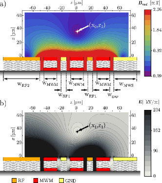
In the first step, we only aim to find a starting geometry that coarsely fulfills the aforementioned field properties, namely an overlap of the magnetic field minimum and the RF null position about above the trap. Here multiple electrode shapes, which differ from the one in Fig. 1c, can be tested. The location of the magnetic field minimum is found to depend most strongly on the spacing between the three MWM segments of length , their width , the width of the left ground electrode and the width of RF2 (see Fig. 3a). Analogously, the RF null position depends on the spacing between RF1 and RF2 as well as their individual widths and . For each iteration the RF null position is calculated using the gapless plane approximation wesenberg_electrostatics_2008 while the behaviour of the magnetic field minimum is inferred from multiple coarse parameter sweeps using the finite-element software. For this specific configuration the spacing between the three MWM segments is kept symmetric, therefore the distance between the segments is equal to two times the gap size plus . No additional residual field cancellations effect have been observed in breaking this symmetry.
Once a coarse geometry has been found, the second step is to perform fine sweeps over all parameters with priority to further minimizing the residual field (even at the cost of an increased mismatch between the RF null and the magnetic field minimum of up to 1-2 ).
In the last step the likely present mismatch is addressed by changing only parameters with a known impact on the magnetic field minimum or the RF null position. For instance, and the width of the large ground electrode can be used to minimize a minimum mismatch along the the -axis, while the upper layer’s thickness mostly affects the magnetic field minimum along the -axis. Due to increased sensitivity requirements, we determine the RF null position in this last step by using finite element simulations with the correct frequency applied to the RF electrode. In our simulation model we consider a final mismach between and of smaller than acceptable.
3.3 Couplings between conductors
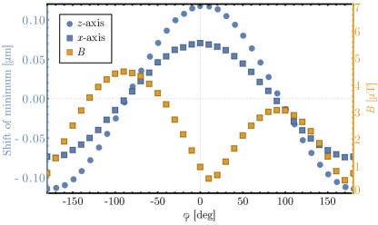
The presence of multiple conductors constitutes a complex problem which the FEM simulation model can not fully account for due to its limited size. The issue arises because of the inductive and resistive coupling between electrodes and the possibility of back reflections of the induced currents in those electrodes. It affects mostly the field configuration created by MWM since any back reflected current can change the magnetic near-field configuration and hence can disturb the overlap with the ion’s position. Since RF and DC are floating electrodes, the effect is negligible. On the other hand, the coupling to the microwave conductors MWC1 and MWC2, see Fig. 1, can cause notable changes of the minimum in MWM magnetic field that depends on coupling parameters and the transmission line of the other conductor wahnschaffe_single-ion_2017 . This can be explained in the following way. The signal in MWM produces currents in MWC1 and MWC2 which propagate along the transmission line of each electrode. Some fraction of these induced currents is backreflected at every impedance variation or imperfection in the transmission line, each with a certain phase depending on the transmission line properties. Once the sum of reflected currents has traveled back to the original electrode, it generates magnetic fields which have to be added to the magnetic field initially produced by MWM, causing an effective shift of the magnetic quadrupole minimum position. The simulation model used here includes only a section of the PCB, so any reflection which does not take place there or on the trap is not accounted for. To evaluate the impact of these reflections we consider a single perfect backreflection from the transmission line which reflects all the current sent to it. The effect is implemented by applying a signal to the corresponding lumped port exactly equal to the power coupled into it by MWM. This constitutes a worst-case scenario since the backreflected current can not be higher than the one originally coupled into an electrode. To understand the possible variation range it is necessary to analyze what happens for different phases of the backreflection. The blue markers (circles for -axis, squares for -axis) in Fig. 4 show the position of the magnetic field minimum as a function of the phase of the backreflected current in MWC2 for a coupling of at an input power of W in MWM (the effect of MWC1 is neglected here for clarity, but would just be added to the field of MWC2). The change of the residual magnetic field at the magnetic minimum position is shown by the orange markers in Fig. 4. Even though for some phases the additional field further suppresses the overall residual field, for most phases the total value of increases.
In the previous trap design mentioned above, the coupling between MWM and the neighbouring microwave conductor, given by the S21 parameter, was simulated to be . The resulting position changes of the magnetic field minimum were up to and made it necessary to minimize the effect by engineering the transmission line appropriately. Since a reason of the strong coupling was found to be the immediate proximity of both involved conductors (compare Fig. 1 in wahnschaffe_single-ion_2017 ), we took special care in the conductor layout of MWC1 and MWC2 in the present multilayer trap. Here, the two microwave conductors are routed around the central DC electrode on each side which minimizes the length of closest proximity and allows a higher spatial separation of MWM and MWC1 by introducing an additional ground electrode of width (see Fig. 3a). Following this approach, the coupling from MWM to MWC1 and MWC2 could be reduced by roughly compared to the previous trap design to simulated values of and , respectively. MWC1 and MWC2 are connected through wirebonds to the filterboard and are grounded at the other end via interconnects in V1, which provide connection to a ground electrode in L1. With the described configuration the coupling could be reduced to a level where its effect can be neglected in the fields overlap predictions, so no further increase of isolation was investigated.
4 Experimental data
To measure the magnetic near-field pattern produced by MWM and compare it to our simulation model, we measure the induced AC Zeeman energy shift on suitable transitions in the atomic hyperfine structure for different ion positions in the radial plane. The exact procedure is detailed in wahnschaffe_single-ion_2017 and based on previous work Warring_2012 . The basic idea is to off-resonantly excite MWM between two pulses of a standard Ramsey experiment and to measure the induced AC Zeeman shift on the transitions (qubit) and of the electronic ground state by fitting the observed phase accumulations due to the induced transition frequency change. The MWM conductor is excited with a frequency of . While the shift on the qubit transition is mainly induced by the -component of the excitation field, the shift on the other transition is also induced by its -components. Moving the ion along the - and -direction by applying DC potentials allows to map the AC Zeeman energy shifts in the radial plane and to infer the resulting magnetic field distribution produced by MWM.
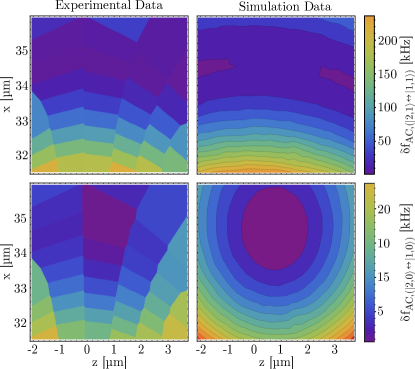
Fig. 5 shows the absolute values of measured AC Zeeman shifts on the qubit transition (upper row) and the transition (lower row) as a function of and around the calculated RF null position at . While the left column displays experimentally measured data, the right column shows AC Zeeman shifts calculated from the magnetic fields obtained by the simulation model introduced in Sec. 3.2. The AC Zeeman shifts of the experimental data and the magnetic field of the simulations are each fitted in a single least squares fit using the 2D quadrupole model of Eq. (2) in wahnschaffe_single-ion_2017 with , , , , , and as fit parameters. Here, is the residual field in the minimum, the magnetic field gradient, the rotation angle of the residual field, the rotation angle of the gradient in the quadrupole, the relative angle between real and imaginary part and (,) the magnetic field minimum position. Since the residual field in the minimum of the experimental data was too low to be fitted accurately, and were manually set to zero in the fit procedure. In consequence, only an upper bound for can be given. A comparison of the fit parameters determined in the experiment and by simulations can be found in Table 1. The upper bound for is obtained by introducing it again in the fitted model as a parameter and by calculating the required to obtain the lowest measured AC Zeeman shift on the transition given by . For the calculation we assume that the measured shift is located at the absolute minimum. The value for is set to since it minimizes the coupling, consequentely giving us an upper boundary for the residual field of . We note that a smaller boundary could possibly be achieved by increasing the spatial resolution of the measurement.
| Parameter [units] | Simulation | Experiment |
|---|---|---|
To induce higher frequency shifts, the data in the lower row was taken and simulated at a nominally higher power level than the data set in the upper row. For reference, the data in the upper row in Fig. 5 corresponds to obtained with of input power to the system.
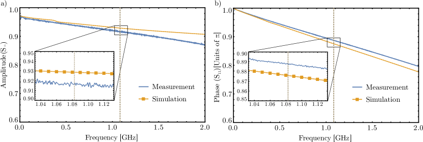
Complementary information can be obtained by analyzing the structure in terms of a microwave circuit. Our full-wave numerical simulations provide the S parameters of the structure for all implemented ports. Using a wafer prober, we can compare this data to actual measurements on fabricated devices (see Fig. 6). Within the frequency regime of interest (around 1 GHz), simulations and experimental data are in good agreement. The deviations for higher frequencies are not relevant for our experiments and can be explained by subtleties of the wafer prober measurements at higher frequencies, where the exact method of contacting the prober to the sample becomes more relevant and slightly deviates from the scenario employed in the simulations. Note that here we re-run the field simulations with all electrodes floating except for MWM and without the filterboard in order to mimic the conditions of the measurement.
5 Summary and conclusion
We have presented a multilayer surface-electrode ion trap based on a novel fabrication technique bautista-salvador_multilayer_2019 . The trap design features two microwave conductors (MWC1, MWC2) to produce a high field amplitude for driving single-qubit gates and one 3D meander-like microwave conductor (MWM) to produce an oscillating near-field gradient with minimal residual field for driving multi-qubit gates around 1 GHz. Besides a general trap characterization, we give detailed information about the employed full-wave simulation model and the design criteria of the microwave conductors in order to produce the desired field configuration. The resulting field pattern of MWM was experimentally measured in a Ramsey-type single-ion experiment and subsequently analyzed in a least square model fit. The extracted 2D quadupole properties of the experimental data were found to be in good agreement with the expected values from our simulation model close to the ion position. The 3D microwave conductor extends to all three fabrication layers and allows an advanced version of a meander-shaped microwave conductor design when compared to a corresponding single-layer design. In the demonstrated multilayer trap, the 3D conductor enables an improved field pattern for multi-qubit gates by further suppressing the residual magnetic field at the ion’s position. For comparison, the lowest residual field at a gradient of in this trap was determined to be while the residual field in a previous single layer design wahnschaffe_single-ion_2017 was calculated to be at least a factor of 14 larger () when scaled to the same gradient. The resulting AC Zeeman shift can cause significant error contributions during multi-qubit gates harty_high-fidelity_2016 and depends on the residual field’s magnitude and polarization. Analyzing the data sets of both traps, we found the absolute lowest measured AC Zeeman shift for the qubit transition in the multilayer trap () to be almost 3 orders of magnitude smaller than in the previous single-layer trap () when scaled to the same gradient.
Assuming the residual field of to be perfectly -polarized we expect at the quadrupole minimum an on-resonance Carrier pi-time longer than for the qubit transition. Based on the measured values of the gradient and the HF radial mode 2, we calculate the minimum time for an entangling gate operation based on the Mølmer-Sørensen interaction sorensen_quantum_1999 ; molmer_multiparticle_1999 to be . Future work will focus on achieving control over the motion at the single-quantum level, measure heating rates and employ such devices for the implementation of entangling gates and effective spin-spin interactions.
Acknowledgements.
We acknowledge support by the PTB cleanroom facility team and funding from PTB, QUEST, LUH, NTH (project number 2.2.11) and DFG through CRC 1227 DQ-mat, project A01.Appendix A Joule heating
When microwave currents are applied to the trap through a conductor with finite conductivity, electric energy is converted into heat through resistive losses. Excessive resistive heating in the trap might lead to a degeneration of its performance or, in extreme cases, to an irreversible damage of the conductor. This is especially critical for an ion trap with multiple layers as discussed here, since current-carrying conductors defined around the geometric trap center have relatively narrow lateral dimensions, i.e. poor thermal contact to the substrate.
To include thermal effects caused by applying short microwave pulses with high power to the MWM conductor imitating real experimental conditions, one would need to numerically solve a complex system, including the whole chip geometry and inductive heating caused on neighbouring electrodes. However, it is also possible to gain insight into thermal effects in the trap design by using a simplified model in which a constant DC current is applied to MWM. As already introduced in Sec. 3.1, we make use of a pocket in the three segments of MWM with length in order to further decrease the residual magnetic field at the ion’s position. Since we are interested in a compromise between a sufficiently low heat load and low , the simplified DC power model still reveals the qualitative behaviour of the system.
In the experiment we apply we apply W to the MWM structure corresponding to c.a. mW of power not reflected by the trap given the measured S-parameter, see caption of Fig. 6. To better understand the limits of thermal dissipation we perform simulations on a DC current in a similar structure. We use a current of A which corresponds to a dissipated power of mW since the nominal geometry considered in the model, , has a resistance of .
The numerical simulations are performed using the AC/DC and heat transfer modules of COMSOL 4.3, assuming a DC current of applied to MWM, supported on an Si3N4/Si substrate of . We perform a parametric sweep of along the -axis. As a result of the fabrication process, the pockets are filled with a dielectric material, which we included in the model assuming a thermal conductivity of . The electrical and thermal properties of Au (conductor material) and Si3N4 (wafer material) are taken from the built-in materials data library. While the room temperature () reference is defined to be at the backside of the chip trap, the temperature of MWM is monitored on the surface of L2 at the geometric trap center marked as ‘X’ in Fig. 1c. At this position the heat load is maximal because each segment of MWM vertically splits into two parts of thickness and , respectively, separated by the pocket of thickness in the interconnect layer V1 filled with the dielectric material (see inset Fig. 1c). Naturally, at this point the heat will be poorly transported along the -axis perperdicular to the trap.
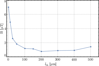
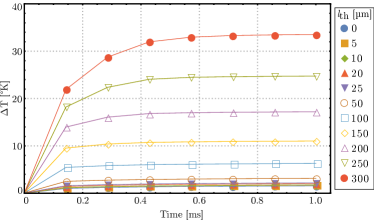
Fig. 7 shows the resulting temperature change with respect to room temperature for different values of as a function of time. For , the system reaches a steady state after , inscreasing its temperature by . As shorter values for decrease the temperature change, but increase at the ion position (see Sec. 3.1), we found to be the best compromise as illustrated in Fig. 8.
References
- (1) J. I. Cirac and P. Zoller, Phys. Rev. Lett. 74,4091 (1995)
- (2) R. Blatt and D. Wineland, Nature 453, 1008 (2008)
- (3) I. M. Georgescu, S. Ashhab and F. Nori, Rev. Mod. Phys. 86,153 (2014)
- (4) A. Bermudez, X. Xu, R. Nigmatullin, J. O’Gorman, V. Negnevitsky, P. Schindler, T. Monz, U. Poschinger, C. Hempel,J. Home, F. Schmidt-Kaler, M. Biercuk, R. Blatt, S. Benjamin and M. Müller, Phys. Rev. X 7,041061 (2017)
- (5) A. Montanaro, npj Quantum Inf. 2,15023 (2016)
- (6) S. Debnath, N. M. Linke, C. Figgatt, K. A. Landsman, K. Wright and C. Monroe, Nature 536, 63 (2016)
- (7) T. Monz, D. Nigg, E. A.Martinez, M. F.Brandl, P. Schindler, R. Rines, S. XWang, I. L. Chuang and R. Blatt, Science 351, 1068 (2016)
- (8) J. Zhang, G. Pagano, P. W. Hess, A. Kyprianidis, P. Becker, H. Kaplan, A. V. Gorshkov, Z.-X. Gong and C. Monroe, Nature 551, 601 (2017)
- (9) P. Jurcevic, H. Shen, P. Hauke, C. Maier, T. Brydges, C. Hempel, B. Lanyon, M. Heyl, R. Blatt and C. Roos, Phys. Rev. Lett. 119,080501 (2017)
- (10) C. Monroe and J. Kim, Science 339,1164 (2013)
- (11) S. Seidelin, J. Chiaverini, R. Reichle, J. J. Bollinger, D. Leibfried, J. Britton, J. H. Wesenberg, R. B. Blakestad, R. J. Epstein, D. B. Hume,W. M. Itano, J. D. Jost, C. Langer, R. Ozeri, N. Shiga, and D. J. Wineland, Phys. Rev. Lett. 96, 253003 (2006)
- (12) D. J. Wineland, C. R. Monroe, W. M. Itano, D. Leibfried, B. E. King and D. M. Meekhof, J. Res. NIST 103, 259 (1998)
- (13) D. Kielpinski, C. Monroe and D. J. Wineland,Nature 417, 709 (2002)
- (14) J. M. Amini, H. Uys, J. H. Wesenberg, S. Seidelin, J. Britton, J. J. Bollinger, D. Leibfried, C. Ospelkaus, A. P. VanDevender, and D. J. Wineland, New J. Phys. 12, 033031 (2010)
- (15) D. P. L. A. Craik, N. M. Linke, T. P. Harty, C. J. Ballance, D. M. Lucas, A. M. Steane and D. T. C. Allcock, App. Phys. B 114, 3 ( 2014)
- (16) N. D. Guise, S. D. Fallek, K. E. Stevens, K. R. Brown, C. Volin, A. W. Harter, J. M. Amini, R. E. Higashi, S. T. Lu, H. M. Chanhvongsak, T. A. Nguyen, M. S. Marcus, T. R. Ohnstein and D. W. Youngner, J. Appl. Phys.117, 174901 (2015)
- (17) P. L. W. Maunz, Techn. Rep. Sandia National Lab. SAND-2016-0796R (2016)
- (18) C. Ospelkaus, C. E. Langer, J. M. Amini, K. R. Brown, D. Leibfried and D. J. Wineland, Phys. Rev. Lett. 101, 090502 (2008)
- (19) F. Mintert and C. Wunderlich, Phys. Rev. Lett. 87 257904 (2001)
- (20) J. Gaebler, T. Tan, Y. Lin, Y. Wan, R. Bowler, A. Keith, S. Glancy, K. Coakley, E. Knill, D. Leibfried and D. J. Wineland, Phys. Rev. Lett. 117 060505 (2016)
- (21) C. Ballance, T. Harty, N. Linke, M. Sepiol and D. Lucas, Phys. Rev. Lett. 117 060504 (2016)
- (22) M. Johanning, A. Braun, N. Timoney, V. Elman, W. Neuhauser and C. Wunderlich, Phys. Rev. Lett. 102 073004 (2009)
- (23) T. Harty, M. Sepiol, D. Allcock, C. Ballance, J. Tarlton and D. Lucas, Phys. Rev. Lett. 117 140501 (2016)
- (24) C. Ospelkaus, U. Warring, Y. Colombe, K. R. Brown, J. M. Amini, D. Leibfried and D. J. Wineland, Nature 476 181 (2011)
- (25) A. Khromova, C. Piltz, B. Scharfenberger, T. F. Gloger, M. Johanning, A. F. Varón and C. Wunderlich, Phys. Rev. Lett. 108 220502 (2012)
- (26) S. Weidt, J. Randall, S. Webster, K. Lake, A. Webb, I. Cohen, T. Navickas, B. Lekitsch, A. Retzker, and W. Hensinger, Phys. Rev. Lett. 117 220501 (2016)
- (27) R. Ozeri, W. M. Itano, R. B. Blakestad, J. Britton, J. Chiaverini, J. D. Jost, C. Langer, D. Leibfried, R. Reichle, S. Seidelin, J. H. Wesenberg and D. J. Wineland, Phys. Rev. A 75 042329 (2007)
- (28) T. Harty, D. Allcock, C. Ballance, L. Guidoni, H. Janacek, N. Linke, D. Stacey and D. Lucas, Phys. Rev. Lett. 113 220501 (2014)
- (29) M. Wahnschaffe, H. Hahn, G. Zarantonello, T. Dubielzig, S. Grondkowski, A. Bautista-Salvador, M. Kohnen and C. Ospelkaus, Appl. Phys. Lett. 110 034103 (2017)
- (30) A. Bautista-Salvador, G. Zarantonello, H. Hahn, A. Preciado-Grijalva, J. Morgner, M. Wahnschaffe and C. Ospelkaus, New Phys. J. 21 043011 (2019)
- (31) J. H. Wesenberg, Phys. Rev. A 78 063410 (2008)
- (32) D. R. Leibrandt, R. J. Clark, J. Labaziewicz, P. Antohi, W. Bakr, K. R. Brown, and I. L. Chuang, Phys. Rev. A 76 055403 (2007)
- (33) H.-Y. Lo, J. Alonso, D. Kienzler, B. C. Keitch, L. E. d. Clercq, V. Negnevitsky, and J. P. Home, Appl. Phys. B 114 17 (2013)
- (34) A. C. Wilson, C. Ospelkaus, A. P. VanDevender, J. A. Mlynek, K. R. Brown, D. Leibfried and D. J. Wineland, Appl. Physics B 105 741 (2011)
- (35) M. Carsjens, M. Kohnen, T. Dubielzig, and C. Ospelkaus, Appl. Phy. B 114 243 (2014)
- (36) Q. A. Turchette, D. Kielpinski, B. E. King, D. Leibfried, D. M. Meekhof, C. J. Myatt, M. A. Rowe, C. A. Sackett, C. S. Wood, W. M. Itano, C. Monroe and D. J. Wineland, Phys. Rev. A 61 063418 (2000)
- (37) U. Warring, C. Ospelkaus, Y. Colombe, R. Jördens, D. Leibfried, D. J. Wineland, Phys. Rev. A 87, 013437 (2013)
- (38) A. Sørensen and K. Mølmer, Phys. Rev. Lett. 82 1971 (1999)
- (39) K. Mølmer and A. Sørensen, Phys. Rev. Lett. 82 1835 (1999)