Charge and Spin Transport Anisotropy in Nanopatterned Graphene
Abstract
Anisotropic electronic transport is a possible route towards nanoscale circuitry design, particularly in two-dimensional materials. Proposals to introduce such a feature in patterned graphene have to date relied on large-scale structural inhomogeneities. Here we theoretically explore how a random, yet homogeneous, distribution of zigzag-edged triangular perforations can generate spatial anisotropies in both charge and spin transport. Anisotropic electronic transport is found to persist under considerable disordering of the perforation edges, suggesting its viability under realistic experimental conditions. Furthermore, controlling the relative orientation of perforations enables spin filtering of the transmitted electrons, resulting in a half-metallic anisotropic transport regime. Our findings point towards a co-integration of charge and spin control in a two-dimensional platform of relevance for nanocircuit design. We further highlight how geometrical effects allow finite samples to display finite transverse resistances, reminiscent of Spin Hall effects, in the absence of any bulk fingerprints of such mechanisms, and explore the underlying symmetries behind this behaviour.
I Introduction
An anisotropic electronic transport response in a system, where the ease with which electrons flow depends on the measurement direction, is an important and challenging concept with a number of key potential applications. Such a behavior can be used to engineer electronic circuits and waveguides Areshkin and White (2007), optical circuits Kim and Choi (2011), and communications devices Yan et al. (2012). It is particularly promising in two-dimensional materials, where the reduced dimensionality allows significant tuning of their electronic properties with only minor structural modifications Pedersen et al. (2008); Yuan et al. (2013); Pedersen et al. (2014); Power and Jauho (2014); Gregersen et al. (2016, 2017); Son et al. (2017). Indeed, much of the recent excitement surrounding monolayer black phosphorus, or phosphorene, relates to its intrinsic electronic anisotropy arising from a buckled geometry Qiao et al. (2014); Liu et al. (2014). However, the high chemical reactivity of phosphorene presents a significant obstacle to its incorporation in devicesZiletti et al. (2015); Koenig et al. (2014), and another strategy for implementing two-dimensional electronic anisotropy needs to be envisioned. One possibility is to induce anisotropic behavior in an otherwise isotropic material. Graphene is the most natural candidate for such an approach due to its exceptional electronic quality, ease of fabrication and electronic measurement, and a range of constantly improving patterning and etching techniques Castro Neto et al. (2009); Novoselov et al. (2012); Ferrari et al. (2015).
Anisotropic transport has been experimentally demonstrated in graphene under strain Pereira et al. (2009); Kim et al. (2009), in graphene sheets with periodic nanofacets Odaka et al. (2010), and has been suggested in anisotropically arranged graphene antidot lattices Pedersen et al. (2014). The latter case consists of an array of perforations, or antidots, whose spacing is different along the and directions. All these methods introduce a system-wide physical anisotropy into the graphene sheet to break the equivalence of transport in the and directions. In this work we consider an alternative patterning approach based on uniformly distributed perforations, where the anisotropic behavior is dictated by the atomic-level properties of the perforation edges.
Extended edges with the zigzag (zz) geometry locally break sublattice symmetry, leading to the formation of localized states Nakada et al. (1996); Wang et al. (2016), and to the formation of local magnetic moments when electron-electron interactions are considered Son et al. (2006); Yu et al. (2008); Yazyev (2010); Han et al. (2014); Roche et al. (2015). Local moments of opposite sign occur at the edges associated with different sublattices, so that global ferromagnetism can only occur when the overall sublattice symmetry is broken Son et al. (2006); Wimmer et al. (2008); Saffarzadeh and Farghadan (2011), in accordance with Lieb’s theorem Lieb (1989). This does not occur for zz-edged nanoribbons Pisani et al. (2007) or perforations containing edges equally divided between the sublattices Trolle et al. (2013). However, the three edges of a zz-edged triangular graphene antidot (zz-TGA) are all associated with a single sublattice, which dictates large ferromagnetic moments Zheng et al. (2009); Sheng et al. (2010); Potasz et al. (2012); Hong et al. (2016); Khan et al. (2016); Gregersen et al. (2016) (see Fig. 1).
Recent works have demonstrated that lattices of approximately side length zz-TGAs provide an excellent platform for electronic and spintronic applications due to robust band gaps, half-metallicity, and spin-splitting propertiesGregersen et al. (2016, 2017). In the case of spin-splitting, incoming currents can be directed into output leads according to their spin orientation. Such behavior is analogous to the spin Hall effectCresti et al. (2016), but without relying on spin-orbit coupling (SOC) effects. These features were shown to be robust against disorder, unlike those in other antidot geometries, due to their dependence on local symmetry breaking effects and cumulative scattering from multiple antidots, and not on the exact separation and size of perforations. With state-of-the-art lithographic methods, triangular holes in graphene Auton et al. (2017), as well as zz-etched nanostructures Shi et al. (2011); Oberhuber et al. (2013); Stehle et al. (2017), can be realised. Alternatively, a patterned layer of hexagonal boron nitride, into which triangular holes can be naturally etched with a large degree of control Stehle et al. (2017), could be employed as a lithographic mask. Many fabrication methods which give precise edge control require seeding, so that the exact distribution of features can be difficult to control. Accounting for a random positioning of triangular defects is therefore crucial for realistic predictions in such systems. Recently, bottom-up techniques have also been developed which can independently give rise to perfect zigzag edgesRuffieux et al. (2016) or perforationsMoreno et al. (2018), suggesting that further development in this field may allow a combination of these features in a given sample.
Here we present simulations which demonstrate how the scattering properties of zz-TGAs also give rise to a significant transport anisotropy—namely a higher conductivity is observed for the armchair (ac) than the zigzag direction. Furthermore, inspired by the spin Hall-like transport behavior in finite TGA superlattice devices Gregersen et al. (2017), we also examine their bulk analog by calculating off-diagonal Hall conductivities. Negligible values are obtained for both the charge and spin conductivities, contrasting with non-zero Hall-like transport in certain device geometries. Using time-reversal symmetry (TRS) arguments, we reconcile these seemingly contradictory results and highlight the role they may play in experiment. We consider zz-TGAs with side lengths , which are distributed randomly throughout the sample. Two small sections of our simulated samples are depicted in Fig. 1(a) and (b), with red and blue triangles denoting individual zz-TGAs. With a homogeneous distribution (with respect to the and directions), anisotropic features originate solely from the edge structure of the zz-TGAs. The strong positional disorder and broken translational invariance in all the simulated samples closely resembles what could be produced, for example, using seeded growth and selective edging techniques. Furthermore, we separately consider more experimentally relevant conditions by including significant side length and edge disorder, and comparing these systems to those with individually precise zz-TGAs.
Disordered systems, containing millions of atoms and hundreds of structural perforations, are simulated using a combination of mean-field Hubbard approaches for individual zz-TGAs and large-scale quantum transport methods to study composite systems. The electronic behavior is analysed using the Chebyshev expansion of the density of states (DOS) Weiße et al. (2006); Roche (1999), while the longitudinal Roche and Mayou (1997); Lherbier et al. (2008); Roche et al. (2012); Torres et al. (2014) and transverse García et al. (2015); Garcia and Rappoport (2016); Cresti et al. (2016) conductivities are computed using the Kubo-Greenwood formalism. The Kubo method gives direct access to both the diagonal conductivities and , from which the charge transport anisotropy can be measured, and the off-diagonal conductivities , which can be connected to measurements of the spin Hall effect. Further details of the geometry and simulation methodologies are presented in Section II, after which we consider the most general case of randomly oriented triangles in Section III. Here we find that a significant anisotropy arises in the electronic transport, with identical behavior for each spin channel. Upon considering triangles with the same alignment in Section IV, a marked increase in the strength of the anisotropy is obtained, with the emergence of a robust half-metallicity, hence yielding a spin-selective anisotropic transport behavior. In Section V, we discuss the off-diagonal conductivity and reconcile the zero signal observed here with the previously predicted spin-Hall type behavior for zz-TGAs in a finite device geometry. We conclude by summarising and discussing our findings in light of recent developments in the field, particularly those investigating spin transport mechanisms in graphene-based systems.
II Geometry and model
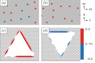
We consider samples of approximately , which are periodic in both dimensions, and contain 400 randomly embedded zz-TGAs and almost 5 million atoms. Small sections from two of our samples are illustrated schematically in Fig. 1(a) and (b). The sample in Fig. 1(a) illustrates the most general distribution, where not only the position, but also the orientation, of each triangle is randomised. The sixfold symmetry of the graphene lattice allows for only two possible orientations of zz-TGAs. Each orientation exposes zz-edges from different sublattices and, in turn, the two orientations exhibit magnetic moments of opposite sign. We use red and blue coloring throughout this work to represent the spin up and down orientation, respectively. The sample in Fig. 1(b) shows the case where all the triangles are aligned and have the same magnetic orientation. Note that the () axis in this work is aligned with a high symmetry zz (ac) direction of the underlying graphene lattice.
All samples discussed in this work contain randomly positioned zz-TGAs. However, we also compare the cases when individual perforations are either pristine or disordered by including side length variations and edge roughness. In the pristine case, the zz-TGAs have side length (), where the graphene lattice constant is , and in the disordered case we consider side lengths in the range . This size allows us to determine if properties predicted in small systems persist to larger scales, whilst also allowing a large number of triangles to be included in the system. Edge-disordered TGAs undergo a further simulated etching, where edge atoms are removed with probability . This etch is performed times. Previous studies Gregersen et al. (2017) indicate that side-length variation has only a minor impact on the qualitative transport-scattering mechanisms of small-scale zz-TGAs. On the other hand, edge disorder has a more dramatic effect, reducing the corresponding magnetic moment distributions and affecting the spin-polarization properties.
The calculations are performed using a nearest-neighbor tight-binding model Hamiltonian
| (1) |
where () is the creation (annihilation) operator for spin on site . The hopping parameter is for neighbors and , and zero otherwise. No spin-orbit terms are included in the calculation. Local magnetic moments are included via spin-dependent on-site energies , with for and for . The on-site magnetic moments are calculated from a self-consistent solution of the Hubbard model within the mean field approximation, , where is the number operator. The magnetic moment distributions for individual triangles are calculated in periodic systems using unit cells (approximately ), which are then embedded into the larger samples. A minimum separation of is imposed between neighboring triangles, which prevents the unit cells used in the mean-field parameterization of individual perforations from overlapping. The on-site Hubbard parameter is set as , which gives good agreement with ab initio calculations in the case of graphene nanoribbons Yazyev (2010).
The atomic structure of two such edge-disordered zz-TGAs and their associated magnetic moments are displayed in Fig. 1(c) and (d). Note that the orientations of the TGAs in Fig. 1(c) and (d) are rotated with respect to one another, which in turns yields oppositely spin-polarized edges. While in one case, Fig. 1(c), all three edges still display significant magnetic moments, in the other case, Fig. 1(d), significantly lowered magnetic moments are seen. A small number of TGAs in our samples will have a considerable quenching of the magnetic moments along one or more of their edges.
The DOS is determined using the efficient linear-scaling kernel polynomial method Weiße et al. (2006) with the Jackson Kernel, and a spectral resolution of approximately . The conductivity tensor is determined within the linear response regime, using the Kubo-Bastin formulaBastin et al. (1971):
| (2) |
where E the Fermi energy, the advanced Green’s function, the Dirac’s delta function and the -component of the velocity operator. The off-diagonal elements are computed numerically by using an efficient linear-scaling algorithm based on the kernel polynomial method García et al. (2015); Cresti et al. (2016). For the diagonal elements, Eq. (2) simplifies to the Kubo-Greenwood formula, where a more efficient real-space time-dependent wavepacket propagation method Roche and Mayou (1997); Lherbier et al. (2008); Roche et al. (2012); Torres et al. (2014) is applicable. In this approach, a random wavepacket is injected into the system. In the presence of disorder, the propagation of the packet quickly becomes diffusive. In such situations, one can relate the time evolution of the mean square displacement operator Torres et al. (2014) to the diffusive coefficient
| (3) |
which can finally be used to compute the conductivity by the means of Einstein’s relation
| (4) |
where the density of states, and is a timescale-dependent conductivity. The semiclassical conductivity is obtained when the diffusion coefficient reaches a saturation limit (maximum value), where , whereas at longer times localization effects start to dominate and suppress the conductivity, eventually leading to an insulating behavior. This method also allow for exploring both limits by exploiting the relation between the effective system size and the mean square displacement , which permits us to select sizes that are much larger than the mean free path but shorter than the localization lengthTorres et al. (2014).
III Randomly oriented triangles
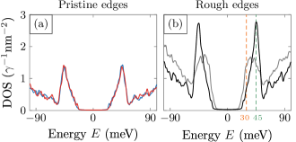
We first consider the case illustrated in Fig. 1(a), where both the position and orientation of the triangles are randomized. Each (spin) orientation occurs with the same probability and, as expected, we find no significant spin-dependence in either the DOS or transport results. For the case without edge disorder, the spin-up and spin-down DOS (red and blue curves, respectively) in Fig. 2(a) are almost exactly superimposed, and they have half the value of the total DOS (black curve) displayed in Fig. 2(b). Minor differences between the spin channels become negligible as the system size is further increased. The system displays semi-conducting behavior, with a gap of approximately . Similar band gap and spin-unpolarized behavior has been demonstrated for periodic superlattices Gregersen et al. (2016), but emerges here for a completely random distribution of antidots. Including edge-disorder, as in the gray curve of Fig. 2(b), results in a qualitatively similar total DOS (dashed curve) with only a slight reduction of the semiconducting gap. This extraordinary robustness against disorder is in stark contrast to, for example, the band-gap formation in lattices of circular or hexagonal antidots, which is very sensitive to fluctuations in the lattice periodicity or antidot shape Yuan et al. (2013); Power and Jauho (2014). This robust band gap was previously studied for small-sized TGA superlattices Gregersen et al. (2016), but here it survives even without the constraint of a superlattice. In Fig. 2(b) we highlight the energies (orange) and (green), near the band-edge and peak of the non-zero DOS region respectively, which will be considered in more detail below.
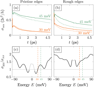
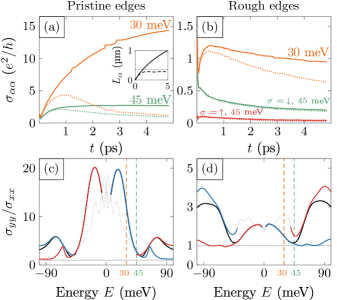
The electronic transport for randomly-oriented zz-TGA systems is examined for both pristine and rough-edged triangles. The time-dependent conductivity gives access to the different transport regimes emerging during the time evolution. Since both spins contribute equally, we consider only the total (charge) conductivity . The - (dotted) and - (solid) direction longitudinal conductivities for are given in the top panels of Fig. 3 for and . In all cases the conductivities reach a maximum value at short times , implying the onset of a diffusive regime, whereas localization effects enter into play at longer times. Lherbier et al. (2008); Ortmann et al. (2011) We note that the graphene sections between perforations in our systems are pristine, so that at extremely short time scales the wave packet can explore this region with an extremely high conductivity, seen as sharp peaks near in our simulations. We neglect this regime throughout our discussion, which focuses on the effects introduced by the zz-TGAs. The emergence of a transport anisotropy is clear by comparing the solid and dashed lines for the same energy, and it is particularly significant for the higher energy (green) case in the presence of disordered edges (Fig. 3(b)). The anisotropies at the maximum simulation time are displayed in Fig. 3(c) and Fig. 3(d), for the pristine and disordered cases respectively, as a function of energy. The faded sections of the curves correspond to the gapped regions of the DOS [see Fig. 2(b)], where the individual conductivities and are nearly zero, and the anisotropy is not well-defined.
In both Fig. 3(c) and (d) the transport anisotropy tends towards at energies far from the gap, and decreases towards unity at the band edges near the gap. Generally, the anisotropy lies above unity (), signifying a preferred ac () transport direction. Electronic states near the band edges in zz-TGA systems are primarily localized near the edges of the TGAs, whereas states further inside the continuum tend to be more homogeneously dispersed Gregersen et al. (2016). Away from the gap, the anisotropy can be explained by a scattering of these more dispersive states by the TGAs which is stronger for currents along the zz-direction than those in the ac-direction. Near the band edges, though, the electronic states are less dispersive and display a lower conductivity. Furthermore, the current in this case is carried by highly localized states near the triangular edges, so that pristine-edged triangles present very little scattering and result in a nearly isotropic transport regime. It is interesting to note that the anisotropy is, in fact, larger for the sample which includes edge disorder. Disordered edges degrade transport more along the zz () directions, because this direction aligns with long nanoribbon-like edges, whose transmission channels are reduced significantly by disorder. Edge-disordered samples are inevitable in realistic systems, where position, orientation, and edge roughness will be difficult to control. It is reassuring that a homogeneous distribution of zz-TGAs, with random orientations and edge disorder, displays such a strong transport anisotropy.
IV Half-metallic aligned samples
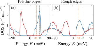
We now consider systems with all triangles aligned in the same direction, so only edges from one sublattice are exposed and all triangles have magnetic moments of the same orientation, as in Fig. 1(b). The spin-polarized DOS for pristine and disordered edges are shown in Fig. 4(a) and (b), respectively, where spin-up and spin-down DOS are displayed by separate red and blue curves. An almost perfect spin polarized DOS is observed within , with opposite spin polarizations on either side of . These half-metallic regions are separated by a band gap of approximately . Just as in the case of randomly-oriented triangles, the band gap and spin-polarization trends are similar to previous results in superlattices.Gregersen et al. (2016) The inclusion of edge defects does not affect the qualitative behavior, i.e. we still find two oppositely spin-polarized, half-metallic regions separated by a small band gap. The principal effect of edge disorder is a slight smearing of the DOS features. It is worth emphasizing that the near perfect half metallicity is exceedingly robust considering that it emerges from a random distribution of edge-disordered antidots.
Electronic transport simulations, without edge-disorder, reveal a large anisotropy, illustrated by the spin-down conductivities at the energies and in Fig. 5(a). The spin-up conductivity (not shown) is mostly zero at these energies due to half-metallicity. The transport anisotropy is particularly large for the case. Here the (ac-direction, solid orange curve) shows quasi-ballistic behavior, i.e. a sub-linear increase, and, no sign of saturation within the accessible time range of 5 ps. Meanwhile for the case saturates to a diffusive, constant value. For both energies localizes quickly at . The simulations are stopped at 5 ps, at which time the simulation length for the case (solid curve in the inset of Fig. 5(a)), exceeds the sample size . When the simulation wave-packets become larger than the simulation samples, artifacts may develop originating solely from the periodic boundary conditions used. The remaining conductivities in Fig. 5(a) have corresponding wavepacket propagation lengths below (the -direction case at is shown by the dashed line in the inset).
The conductivity anisotropies of the sample without edge-disorder, at the maximum simulation time , are displayed in Fig. 5(c). The spin-up and spin-down anisotropies are displayed by separate red and blue curves, with the total charge anisotropy shown in black. The individual anisotropies are ill-defined in the dotted sections where conductivities and vanish. The anti-symmetry in Fig. 5(c) between the two spin channels originates from the anti-symmetric DOS [see Fig. 4(a)]. Fig. 5(c) reveals a maximum anisotropy (for spin-down) near , with . This corresponds to the onset of states which are largely localized on the zz-edges, but have some penetration into the surrounding graphene Gregersen et al. (2016). A comparison with the more isotropic transport found for random TGA orientations [see Fig. 3(c)] suggests that localised states at TGAs with the same orientation couple quite strongly to form robust transport channels along the ac direction. The anisotropy for spin-down decreases towards larger energies, but never reaches values below unity, and transport in the ac direction is always preferred. At higher energies still, the onset of spin-up states (red curve, see also Fig. 4(a)) of a similar, but more dispersive, nature than their lower-energy spin-down counterparts gives a less massive, but still significant, anisotropy . The total charge anisotropy (black curve) is lowest at the crossover between the spin-down and spin-up regimes. Most importantly, since low-energy transport is driven by coupling between states localised near zz-TGAs, and not bulk-states which can be scattered by them, a quasi-ballistic regime emerges in which extremely large anisotropies are present.
The decrease in conductivity on including edge disorder is most evident for the case (orange curves) in Fig. 5(b). Now both (solid) and (dotted) saturate near and afterwards begin to localize. The conductivities saturate even earlier, and the maxima cannot be resolved. All simulation lengths now remain within the sample size (not shown). Earlier onset of localized behavior was also observed in Fig. 3(b) for randomly-aligned triangles, and can be attributed to a degradation of transport mediated by channels near the triangle edges by scattering due to edge roughness. The anisotropies of the edge-disordered sample are displayed in Fig. 5(d) at the maximum simulation time . These show a continued preference for ac-direction transmission, as they again remain above unity. However, the maximum is much smaller than the pristine case a reduction to for the spin-down channel. However, the higher-energy up-spin transport suffers a less dramatic reduction and takes values at . The rough edges significantly quench electronic transport near the band edges, although not enough to completely remove the transport anisotropy. However, the higher-energy states are more dispersed and thus less sensitive to edge roughness. We note that controlling the orientation of a random distribution of zz-TGAs allows for behavior with huge potential for spintronic applications – namely a device whose spin-polarization and degree of anisotropy is tunable by gate voltage. Furthermore, this behavior remains qualitatively similar under reasonable disorder of the triangle edges. Considering only the total charge current (black curve in Fig. 5( d)), we note that aligned triangles give a similar anisotropy to the randomly aligned case, but with a somewhat greater magnitude. This suggests that such setups may be interesting even for electronic devices which neglect the spin properties underpinning their anisotropic transport behavior.
V Off-diagonal conductivities
The anisotropic transport discussed so far emerges due to a geometric asymmetry—the - and -directions in the lattice have a different alignment relative to the zigzag edge segments. A strong anisotropy then arises when transport is mediated by electronic states associated with these edges. Edge magnetism can then further lead to a strong spin-dependent behavior.
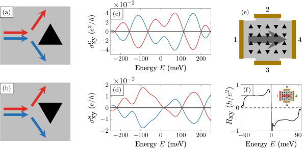
A similar spin-dependent geometric asymmetry can be observed in the electronic scattering profile of zz-TGAs. Electrons incident along the -direction display radically different scattering probabilities in the or directions due to the broken reflection symmetry inherent in the triangular shape. In a previous work Gregersen et al. (2017), we demonstrated how zz-TGA devices may be engineered to exploit this property to spatially split spins according to their orientation, as shown in Fig. 6(a) and (b). In certain geometries, non-zero transverse resistances could be induced. These behaviors suggest analogies with the Spin Hall and inverse Spin Hall effects (SHE/iSHE), which induce similar results when spin-orbit coupling (SOC) terms are included.
These effects can be simulated in both finite device geometries, using Landauer-Büttiker methods, and in bulk systems, using the Kubo-Bastin approach. Transverse resistances and spin currents, corresponding directly to experimentally-measurable quantities, emerge from multi-terminal simulations and are associated with the off-diagonal elements of the bulk conductivity tensor, . This quantity captures the intrinsic response of the system, and unlike the Hall resistance , it is independent of the measurement geometry or device setup. The off-diagonal matrix elements of the conductivity () and resistivity () tensors are connected by
| (5) |
from which we note that their zeros coincide in conducting systems. The Onsager reciprocity relation forces the off-diagonal elements of the conductivity tensor to be zero unless time-reversal symmetry (TRS) is broken. However, even in cases when TRS is preserved, the off-diagonal tensor elements are not necessarily trivial once we consider individual spin channels. Treating the spin channels as separate, non-interacting systems, SOC enters as an effective magnetic field which breaks TRS in each channel independently, giving finite and . However, the two spin channels form a time-reversal symmetric pair and contribute equally but oppositely to the off-diagonal conductivity, i.e. . The total, or charge, off-diagonal conductivity is then zero, consistent with the conservation of TRS in the system as a whole. However, the spin Hall conductivity is finite.
In the case of zz-TGA structures, the presence of magnetic moments breaks TRS. However, the absence of spin-mixing terms allows the system to once more be considered as two separate, non-interacting spin channels. Our model considers two parallel channels with different (i.e. spin-dependent) potential landscapes, and within each channel, TRS is effectively preserved (up to spin orientation) and thus the individual off-diagonal conductivities and are identically zero. The total off-diagonal conductivity , being a sum of the two spin channel contributions, is also zero despite the broken time-reversal symmetry of the complete system. A full Kubo-Bastin calculation confirms that both the Hall and Spin-Hall conductivities are zero, as shown by the solid black lines in Fig. 6(c) and (d), respectively. However, it is worth pointing out that the stochastic scheme used to compute both conductivities inherently breaks all the system’s symmetries because it connects all its possible subspaces. These symmetries need later to be restored, either by averaging over many random vectors, or by an explicit imposition of the symmetries through a set transformation which cancels additional random noiseMarmolejo-Tejada et al. (2017). In Fig. 6(c,d), we show the result for an arbitrary random vector (blue curve) and note the non-zero, oscillatory behaviour. A large set of random vectors is required for the averaging approach, and the result can display misleading behaviour en route to convergence. Unlike the case of true spin or valley hall effects, we cannot take advantage of an overall TRS in the set transformation approachMarmolejo-Tejada et al. (2017). However, the spin-asymmetry around allows to write an Onsager relationHertel (2012) , and calculate as an average of these two quantities evaluated for a small number of random vectors. is plotted by a red curve in Fig. 6(c,d), and exactly cancels for the same random vector, indicating that the charge and spin Hall conductivities are identically zero.
In finite, multi-terminal devices, the Landauer formula
| (6) |
can be used to calculate the currents () and potentials () at each lead from the transmissions () between leads. To evaluate the transverse resistance in the four-terminal cross-bar shown in Fig. 6(e), we solve this system of equations under the boundary conditions , , , , so that
| (7) |
Restricting our analysis only to the conditions that give rise to a non-zero transverse resistance, we assume from here on that follows , and omit complicating prefactors and denominators. In its most general formButtiker (1988),
| (8) | ||||
and for independent spin channels, each transmission term can be written . Under TRS (), Eq. (8) simplifies to
| (9) |
showing that the transverse resistance can be finite even when the associated resistivity is zero. However, this discrepancy requires asymmetric couplings between sets of probes which we would generally expect to be symmetric (e.g. and ) This can be achieved, for example, by offsetting the top and bottom probes in non-ballistic devices and it is underpinned by a simple conceptual explanation. If the top (or bottom) lead couples identically to the left and right leads, its potential must lie half way between them . Moving the top probe nearer to either the left or right lead changes its potential, and breaking the symmetry between top and bottom probes then gives a finite .
In homogeneous spin-orbit systems, with a symmetric placement of leads, we assume that the transmissions between neighboring leads depends only on their relative alignment, i.e. clockwise (c.) or anti-clockwise (a.c.), and on the spin orientation. Using the identity to relate the two spin channels with SOC, we write
| (10) | ||||
and quickly find from Eq. (9).
No charge current flows in the voltage probes; however a net spin current is possible because spin mixing is allowed in these leads, so that they can absorb and reinject electrons with opposite spin as long as the net charge current is zero. The general expression for the spin current in each lead is
| (11) | ||||
which in its expanded form is quite complicated. For a homogeneous SOC and symmetric leads, using Eq. (10), it simplifies significantly to
| (12) |
– the hallmark transverse spin current of the SHE. All-electrical detection of the SHE usually employs a non-local setup where this spin current generates a potential difference between an additional pair of probes via the inverse Spin Hall effect (iSHE). A similar effect can be demonstrated in the cross geometry [see Fig. 6(e)] by using a ferromagnetic contact as our injector, so that the left lead only injects spin-up electrons, with the other leads unchanged. Setting we find
| (13) |
for TRS SOC pairs, which simplifies to
| (14) |
in the homogeneous, symmetric case. Here the finite potential difference across the device is directly connected to differences between spin-up and spin-down transmission probabilities. Swapping the spin-orientation of the injector changes the sign of the transverse resistance, confirming its spin-related origin.
We now turn back to magnetic triangles, which also induce a spatial splitting of spin channels, but obey a different set of symmetries. As discussed above, each spin channel has a different potential landscape and effectively conserves TRS. Thus , but and , so that the total transmission also obeys , despite the absence of overall TRS. With unpolarized leads, the analysis based on Eq. (9) still holds, and the transverse resistance is zero for symmetric probe configurations. The isotropic condition assumed for SOC cases is no longer a relevant limit here, as geometric anisotropies are essential to the effects studied. However, pristine triangles are symmetric upon reflection in the -axis, and asymmetries due to triangle position and disorder should average out in large enough samples, so it is useful to consider the case of left-right symmetric transmissions. This forces both and —a critical difference between SOC and magnetic-scattering cases. For SOC, each spin channel generates an equal and opposite transverse current leading to a finite spin, but zero charge, current, whereas for zz-TGAs each channel independently preserves TRS, so that neither generates a transverse current and both their sum and difference are zero. Neither scenario generates a non-negligible transverse resistance with non-magnetic leads. With a FM injector lead however, the zz-TGA system generates a non-zero transverse resistance
| (15) |
which simplifies to
| (16) |
under left-right symmetry. The result from a full simulation of this quantity in a cross-device is shown in Fig. 6(f). Finally, we note that this iSHE-type behavior for zz-TGAs emerges in the absence of a corresponding SHE-type behavior for the charge current.
VI Conclusion
We have examined graphene systems patterned with zz-TGAs and demonstrated how large-scale, disordered samples display a range of spatial anisotropies in their charge and spin transport characteristics. Electronic band-gaps are found for both aligned and randomly-oriented triangles, whereas the aligned case also shows a strong half-metallic behaviour, with up- and down- spin electrons dominating transport at opposite sides of half-filling. These properties are robust in the presence of strong edge disorder, and in the absence of a superlattice, where they have previously been predictedGregersen et al. (2016).
We have further demonstrated that such systems display significant anisotropic transport behaviour with respect to the direction of current flow. A strong preference for armchair direction transport is found, leading in certain cases to quasi-ballistic behaviour in one direction and localization in the other, despite a homogeneous distribution of perforations. The qualitative anisotropic trends survive the introduction of edge disorder, suggesting application in realistic devices where a control of the direction of flow of charge current, or spin-polarised current is required.
Triangular perforations can also scatter electrons anistropically in directions perpendicular to the charge current. The generation of a transverse resistance by a spin-polarised current is the essence of the iSHE, and we note that zz-TGAs can give rise to whose functional form (Eq. (16)) is similar to that for the SOC case (Eq. (14)). Furthermore, we note that, for zz-TGAs, the iSHE-type behaviour emerges in the absence of a corresponding SHE-type behaviour for the charge current and zero bulk transverse resistivities. Therefore zz-TGA devices offer the possibility not just to filter different spin channels into different leads, as discussed in Ref. [Gregersen et al., 2017], but of generating a transverse resistance whose sign depends on the spin-polarisation of the input current.
A key feature of zigzag-edge magnetism in graphene is the spin-dependent asymmetry with respect to Fermi energy, so that sweeping through half-filling inverts the role of the two spin channels. This leads to an antisymmetry in the measured with an FM injector, as the spin-polarised current is deflected towards opposite edges of the system for different charge carriers. The symmetry with respect to in standard iSHE setups depends on the type of SOC considered: intrinsic Kane-Mele coupling should present a symmetric signalVan Tuan et al. (2016) whereas Rashba coupling should give an asymmetric signal with a linear transitionChen et al. (2012); Van Tuan et al. (2016) through . This suggests that contributions from zigzag-edge magnetism could result in Rashba-like behaviour being observed in inverse Spin Hall measurements.
Finally, the behaviors discussed here emerge from the presence of two key features in our systems: i) local magnetic defects with a sublattice-dependent antiferromagnetic alignment and ii) geometric asymmetries. These features arise naturally for zz-TGAs, but we note that it may be be possible to generate similar effects, deliberately or inadvertently, in other systems. A number of individual defects, including vacancies, hydrogen adatoms and substitutional species, are predicted to induce local magnetic moments in graphene. The alignment of these moments, through e.g. indirect exchange interactionsSaremi (2007); Power and Ferreira (2013), is expected to be highly sublattice-dependent. Local clustering, or an asymmetric occupation of sublattices, could give rise to the conditions necessary for anisotropic transport or transverse resistance signals. This is perhaps most relevant for hydrogen atoms, which have been proposed as both a source of local magnetismYazyev and Helm (2007); González-Herrero et al. (2016) and of spin-orbit couplingGmitra et al. (2013). Experimental signatures of SHE and iSHE mechanisms have been detectedBalakrishnan et al. (2013), but have also proven difficult to reproduceKaverzin and van Wees (2015), suggesting that a more complex mechanism than a simple enhancement of SOC is at playKochan et al. (2014); Soriano et al. (2015). In this direction, a recent studyOffidani and Ferreira (2018) has also highlighted the importance of the interplay between magnetism, disorder and SOC in determining the exact Hall response in graphene systems.
VII Acknowledgments
S.S.G. acknowledges research travel support from Torben og Alice Frimodts Fond and Otto Mønsted Fonden. S.R.P. acknowledges funding from the European Union’s Horizon 2020 research and innovation programme under the Marie Skłodowska-Curie grant agreement No 665919. J.H.G and S.R. acknowledge funding from the Spanish Ministry of Economy and Competitiveness and the European Regional Development Fund (project no. FIS2015-67767-P MINECO/FEDER, FIS2015-64886-C5-3-P) and the European Union Seventh Framework Programme under grant agreement no. 785219 (Graphene Flagship). The Center for Nanostructured Graphene (CNG) is sponsored by the Danish Research Foundation, Project DNRF103. ICN2 is funded by the CERCA Programme/Generalitat de Catalunya and supported by the Severo Ochoa programme (MINECO, Grant. No. SEV-2013-0295).
References
- Areshkin and White (2007) D. A. Areshkin and C. T. White, Nano Letters 7, 3253 (2007).
- Kim and Choi (2011) J. T. Kim and S.-Y. Choi, Optics Express 19, 24557 (2011).
- Yan et al. (2012) H. Yan, X. Li, B. Chandra, G. Tulevski, Y. Wu, M. Freitag, W. Zhu, P. Avouris, and F. Xia, Nature Nanotechnology 7, 330 (2012).
- Pedersen et al. (2008) T. G. Pedersen, C. Flindt, J. G. Pedersen, N. A. Mortensen, A.-P. Jauho, and K. Pedersen, Physical Review Letters 100, 136804 (2008).
- Yuan et al. (2013) S. Yuan, R. Roldán, A.-P. Jauho, and M. I. Katsnelson, Physical Review B 87, 85430 (2013).
- Pedersen et al. (2014) J. G. Pedersen, A. W. Cummings, and S. Roche, Physical Review B 89, 165401 (2014).
- Power and Jauho (2014) S. R. Power and A.-P. Jauho, Physical Review B 90, 115408 (2014).
- Gregersen et al. (2016) S. S. Gregersen, S. R. Power, and A.-P. Jauho, Physical Review B 93, 245429 (2016).
- Gregersen et al. (2017) S. S. Gregersen, S. R. Power, and A.-P. Jauho, Physical Review B 95, 121406 (2017).
- Son et al. (2017) Y. Son, D. Kozawa, A. T. Liu, V. B. Koman, Q. H. Wang, and M. S. Strano, 2D Materials 4, 025091 (2017).
- Qiao et al. (2014) J. Qiao, X. Kong, Z.-X. Hu, F. Yang, and W. Ji, Nature Communications 5 (2014), 10.1038/ncomms5475.
- Liu et al. (2014) H. Liu, A. T. Neal, Z. Zhu, Z. Luo, X. Xu, D. Tománek, and P. D. Ye, ACS Nano 8, 4033 (2014).
- Ziletti et al. (2015) A. Ziletti, A. Carvalho, D. K. Campbell, D. F. Coker, and A. H. Castro Neto, Phys. Rev. Lett. 114, 046801 (2015).
- Koenig et al. (2014) S. P. Koenig, R. A. Doganov, H. Schmidt, A. Castro Neto, and B. Özyilmaz, Applied Physics Letters 104, 103106 (2014).
- Castro Neto et al. (2009) A. H. Castro Neto, N. M. R. Peres, K. S. Novoselov, and A. K. Geim, Reviews of Modern Physics 81, 109 (2009).
- Novoselov et al. (2012) K. S. Novoselov, V. I. Fal’ko, L. Colombo, P. R. Gellert, M. G. Schwab, and K. W. Kim, Nature (London) 490, 192 (2012).
- Ferrari et al. (2015) A. C. Ferrari, F. Bonaccorso, V. Fal’ko, K. S. Novoselov, S. Roche, P. Bøggild, S. Borini, F. H. L. Koppens, V. Palermo, N. Pugno, J. A. Garrido, R. Sordan, A. Bianco, L. Ballerini, M. Prato, E. Lidorikis, J. Kivioja, C. Marinelli, T. Ryhänen, A. Morpurgo, J. N. Coleman, V. Nicolosi, L. Colombo, A. Fert, M. Garcia-Hernandez, A. Bachtold, G. F. Schneider, F. Guinea, C. Dekker, M. Barbone, Z. Sun, C. Galiotis, A. N. Grigorenko, G. Konstantatos, A. Kis, M. Katsnelson, L. Vandersypen, A. Loiseau, V. Morandi, D. Neumaier, E. Treossi, V. Pellegrini, M. Polini, A. Tredicucci, G. M. Williams, B. Hee Hong, J.-H. Ahn, J. Min Kim, H. Zirath, B. J. van Wees, H. van der Zant, L. Occhipinti, A. Di Matteo, I. A. Kinloch, T. Seyller, E. Quesnel, X. Feng, K. Teo, N. Rupesinghe, P. Hakonen, S. R. T. Neil, Q. Tannock, T. Löfwander, and J. Kinaret, Nanoscale 7, 4598 (2015).
- Pereira et al. (2009) V. M. Pereira, A. H. Castro Neto, and N. M. R. Peres, Physical Review B 80, 045401 (2009).
- Kim et al. (2009) K. S. Kim, Y. Zhao, H. Jang, S. Y. Lee, J. M. Kim, K. S. Kim, J.-H. Ahn, P. Kim, J.-Y. Choi, and B. H. Hong, Nature 457, 706 (2009).
- Odaka et al. (2010) S. Odaka, H. Miyazaki, S.-L. Li, A. Kanda, K. Morita, S. Tanaka, Y. Miyata, H. Kataura, K. Tsukagoshi, and Y. Aoyagi, Applied Physics Letters 96, 062111 (2010).
- Nakada et al. (1996) K. Nakada, M. Fujita, G. Dresselhaus, and M. S. Dresselhaus, Physical Review B 54, 17954 (1996).
- Wang et al. (2016) S. Wang, L. Talirz, C. A. Pignedoli, X. Feng, K. Müllen, R. Fasel, and P. Ruffieux, Nature Communications 7, 11507 (2016).
- Son et al. (2006) Y.-W. Son, M. L. Cohen, and S. G. Louie, Nature 444, 347 (2006).
- Yu et al. (2008) D. Yu, E. M. Lupton, H. J. Gao, C. Zhang, and F. Liu, Nano Research 1, 497 (2008).
- Yazyev (2010) O. V. Yazyev, Reports on Progress in Physics 73, 056501 (2010).
- Han et al. (2014) W. Han, R. K. Kawakami, M. Gmitra, and J. Fabian, Nature Nanotechnology 9, 794 (2014).
- Roche et al. (2015) S. Roche, J. Åkerman, B. Beschoten, J.-C. Charlier, M. Chshiev, S. P. Dash, B. Dlubak, J. Fabian, A. Fert, M. Guimarães, et al., 2D Materials 2, 030202 (2015).
- Wimmer et al. (2008) M. Wimmer, İ. Adagideli, S. Berber, D. Tománek, and K. Richter, Physical Review Letters 100, 177207 (2008).
- Saffarzadeh and Farghadan (2011) A. Saffarzadeh and R. Farghadan, Applied Physics Letters 98, 023106 (2011).
- Lieb (1989) E. H. Lieb, Physical Review Letters 62, 1201 (1989).
- Pisani et al. (2007) L. Pisani, J. A. Chan, B. Montanari, and N. M. Harrison, Physical Review B 75, 064418 (2007).
- Trolle et al. (2013) M. L. Trolle, U. S. Møller, and T. G. Pedersen, Physical Review B 88, 195418 (2013).
- Zheng et al. (2009) X. H. Zheng, G. R. Zhang, Z. Zeng, V. M. García-Suárez, and C. J. Lambert, Physical Review B 80, 075413 (2009).
- Sheng et al. (2010) W. Sheng, Z. Y. Ning, Z. Q. Yang, and H. Guo, Nanotechnology 21, 385201 (2010).
- Potasz et al. (2012) P. Potasz, A. D. Güçlü, A. Wójs, and P. Hawrylak, Physical Review B 85, 075431 (2012).
- Hong et al. (2016) X. K. Hong, Y. W. Kuang, C. Qian, Y. M. Tao, H. L. Yu, D. B. Zhang, Y. S. Liu, J. F. Feng, X. F. Yang, and X. F. Wang, The Journal of Physical Chemistry C 120, 668 (2016).
- Khan et al. (2016) M. E. Khan, P. Zhang, Y.-Y. Sun, S. B. Zhang, and Y.-H. Kim, AIP Advances 6, 035023 (2016).
- Cresti et al. (2016) A. Cresti, B. K. Nikolić, J. H. García, and S. Roche, Riv. del Nuovo Cim. 39, 587 (2016), arXiv:1610.09917 .
- Auton et al. (2017) G. Auton, R. K. Kumar, E. Hill, and A. Song, Journal of Electronic Materials 46, 3942 (2017).
- Shi et al. (2011) Z. Shi, R. Yang, L. Zhang, Y. Wang, D. Liu, D. Shi, E. Wang, and G. Zhang, Advanced Materials 23, 3061 (2011).
- Oberhuber et al. (2013) F. Oberhuber, S. Blien, S. Heydrich, F. Yaghobian, T. Korn, C. Schüller, C. Strunk, D. Weiss, and J. Eroms, Applied Physics Letters 103, 143111 (2013).
- Stehle et al. (2017) Y. Y. Stehle, X. Sang, R. R. Unocic, D. Voylov, R. K. Jackson, S. Smirnov, and I. Vlassiouk, Nano Letters 17, 7306 (2017).
- Ruffieux et al. (2016) P. Ruffieux, S. Wang, B. Yang, C. Sánchez-Sánchez, J. Liu, T. Dienel, L. Talirz, P. Shinde, C. A. Pignedoli, D. Passerone, et al., Nature 531, 489 (2016).
- Moreno et al. (2018) C. Moreno, M. Vilas-Varela, B. Kretz, A. Garcia-Lekue, M. V. Costache, M. Paradinas, M. Panighel, G. Ceballos, S. O. Valenzuela, D. Peña, and A. Mugarza, Science (80-. ). 360, 199 (2018).
- Weiße et al. (2006) A. Weiße, G. Wellein, A. Alvermann, and H. Fehske, Reviews of Modern Physics 78, 275 (2006).
- Roche (1999) S. Roche, Physical Review B 59, 2284 (1999).
- Roche and Mayou (1997) S. Roche and D. Mayou, Physical Review Letters 79, 2518 (1997).
- Lherbier et al. (2008) A. Lherbier, B. Biel, Y.-M. Niquet, and S. Roche, Physical Review Letters 100, 036803 (2008).
- Roche et al. (2012) S. Roche, N. Leconte, F. Ortmann, A. Lherbier, D. Soriano, and J.-C. Charlier, Solid State Communications 152, 1404 (2012), exploring Graphene, Recent Research Advances.
- Torres et al. (2014) L. E. F. F. Torres, S. Roche, and J.-c. Charlier, Introduction to Graphene-Based Nanomaterials: From Electronic Structure to Quantum Transport, 1st ed. (Cambridge University Press, New York, 2014) p. 421.
- García et al. (2015) J. H. García, L. Covaci, and T. G. Rappoport, Physical Review Letters 114, 116602 (2015).
- Garcia and Rappoport (2016) J. H. Garcia and T. G. Rappoport, 2D Materials 3, 024007 (2016), arXiv:1602.04864 .
- Bastin et al. (1971) A. Bastin, C. Lewiner, O. Betbeder-matibet, and P. Nozieres, J. Phys. Chem. Solids 32, 1811 (1971).
- Ortmann et al. (2011) F. Ortmann, A. Cresti, G. Montambaux, and S. Roche, EPL (Europhysics Letters) 94, 47006 (2011).
- Marmolejo-Tejada et al. (2017) J. M. Marmolejo-Tejada, J. H. García, P. H. Chang, X. L. Sheng, A. Cresti, S. Roche, and B. K. Nikolic, ArXiv:1706.09361 , 1 (2017), arXiv:1706.09361 .
- Hertel (2012) P. Hertel, in Contin. Phys., Graduate Texts in Physics (Springer Berlin Heidelberg, Berlin, Heidelberg, 2012) first edit ed., Chap. Examples, pp. 165–169.
- Buttiker (1988) M. Buttiker, IBM Journal of Research and Development 32, 317 (1988).
- Van Tuan et al. (2016) D. Van Tuan, J. M. Marmolejo-Tejada, X. Waintal, B. K. Nikolić, S. O. Valenzuela, and S. Roche, Phys. Rev. Lett. 117, 176602 (2016).
- Chen et al. (2012) C.-L. Chen, Y.-H. Su, and C.-R. Chang, Journal of Applied Physics 111, 07B330 (2012).
- Saremi (2007) S. Saremi, Physical Review B 76, 184430 (2007).
- Power and Ferreira (2013) S. Power and M. Ferreira, Crystals 3, 49 (2013).
- Yazyev and Helm (2007) O. V. Yazyev and L. Helm, Phys. Rev. B 75, 125408 (2007).
- González-Herrero et al. (2016) H. González-Herrero, J. M. Gómez-Rodríguez, P. Mallet, M. Moaied, J. J. Palacios, C. Salgado, M. M. Ugeda, J.-Y. Veuillen, F. Yndurain, and I. Brihuega, Science 352, 437 (2016).
- Gmitra et al. (2013) M. Gmitra, D. Kochan, and J. Fabian, Phys. Rev. Lett. 110, 246602 (2013).
- Balakrishnan et al. (2013) J. Balakrishnan, G. K. W. Koon, M. Jaiswal, A. C. Neto, and B. Özyilmaz, Nature Physics 9, 284 (2013).
- Kaverzin and van Wees (2015) A. A. Kaverzin and B. J. van Wees, Phys. Rev. B 91, 165412 (2015).
- Kochan et al. (2014) D. Kochan, M. Gmitra, and J. Fabian, Physical review letters 112, 116602 (2014).
- Soriano et al. (2015) D. Soriano, D. Van Tuan, S. M. Dubois, M. Gmitra, A. W. Cummings, D. Kochan, F. Ortmann, J.-C. Charlier, J. Fabian, and S. Roche, 2D Materials 2, 022002 (2015).
- Offidani and Ferreira (2018) M. Offidani and A. Ferreira, ArXiv e-prints (2018), arXiv:1801.07713 [cond-mat.mes-hall] .