Inverse-Designed Diamond Photonics
Abstract
Diamond hosts optically active color centers with great promise in quantum computation, networking, and sensing. Realization of such applications is contingent upon the integration of color centers into photonic circuits. However, current diamond quantum optics experiments are restricted to single devices and few quantum emitters because fabrication constraints limit device functionalities, thus precluding color center integrated photonic circuits. In this work, we utilize inverse design methods to overcome constraints of cutting-edge diamond nanofabrication methods and fabricate compact and robust diamond devices with unique specifications. Our design method leverages advanced optimization techniques to search the full parameter space for fabricable device designs. We experimentally demonstrate inverse-designed photonic free-space interfaces as well as their scalable integration with two vastly different devices: classical photonic crystal cavities and inverse-designed waveguide-splitters. The multi-device integration capability and performance of our inverse-designed diamond platform represents a critical advancement toward integrated diamond quantum optical circuits.
Diamond has excellent material properties for quantum optics,Atature2018 ; Awschalom2018 optomechanics,Khanaliloo2015b ; Burek2016 and nonlinear optics.Hausmann2014 Of particular interest is the variety of color centers that diamond hosts, some of which exhibit very long coherence times.Atature2018 ; Rose2018 The development of diamond photonic circuitsAharonovich2011 has emerged as a promising route for implementing optical quantum networks,Cirac1997 ; Briegel1998 ; Kimble2008 ; Bernien2012 ; Sipahigil2012 ; Bernien2013 ; Pfaff2014 ; Hensen2015 ; Gao2015 ; Sun2018 ; Lemonde2018 quantum computers,Ladd2010 ; Sipahigil2016 ; Evans2018 and quantum sensors.Balasubramanian2008 ; Degen2017 However, a major challenge in diamond quantum photonics is the lack of high-quality thin films of diamond, as the production of electronic grade diamond can be achieved only in homoepitaxy, and thinning processes are not repeatable enough for photonic crystal cavity fabrication.Burek2014 As a result, state-of-the-art diamond cavity quantum photonics relies on angled-etching of bulk diamond.Burek2014 This technique naturally leads to triangular cross-sections with strongly constrained geometries, which limit device design and functionality. Recent developments in diamond processing based on quasi-isotropic etchingKhanaliloo2015 ; Mouradian2017 ; Wan2018 ; Mitchell2019 (see Supplementary Note 1, Figure 1 and 2) allow the production of diamond membranes with rectangular cross-sections and variable dimensions from bulk diamond. Although rectangular cross-sections are a major step toward diamond integrated circuits, this fabrication technique comes with its own geometric constraints, such as limitations on the range of fabricable feature sizes, which originate from a strong correlation of the initial etch depth and undercut thin-film area. Traditional photonic designs that do not account for fabrication constraints are thus unable to take full advantage of this new fabrication technique.
In this work, we overcome these fabrication and design challenges by employing inverse design methods. In silicon nanophotonics these methods have recently attracted considerable attention for their efficient design of devices with superior performance over conventional designs.Molesky2018 This optimization technique searches through the full parameter space of fabricable devices, thereby arriving at solutions previously inaccessible to traditional design techniques.Su2018 We showcase the potential of inverse design techniques for diamond integrated circuits by designing and fabricating several devices: A compact vertical coupler, an essential component for large-scale quantum photonic systems, and a small circuit consisting of inverse-designed vertical couplers and waveguide-splitters acting as interfaces for two nanoresonators. Our inverse-designed vertical coupler adheres to the diamond fabrication constraints and outperforms commonly used free-space interfaces. The fabricated devices show excellent agreement with simulations in terms of both performance and yield. In the second example, we illustrate the integration of such a vertical coupler into a diamond photonic circuit consisting of two nanobeam resonators connected via inverse-designed waveguide-splitters – a configuration that could be used to entangle two quantum emitters embedded inside such resonators.
Inverse design of diamond nanophotonic devices
In photonics, grating couplers are frequently used as optical free-space interfaces.Laere2007 ; Vermeulen2010 ; Rath2013 ; Faraon2013 ; Piracha2016 ; Zhou2018 To achieve high coupling efficiencies, such designs typically use asymmetry along the z-axis, e.g. through partial etchesLaere2007 ; Vermeulen2010 ; Zhou2018 or material stacks with varying refractive indices.Vermeulen2010 In diamond quantum photonics many of these approaches cannot be employed because current thin-film diamond on silica substrate platformsRath2013 ; Faraon2013 ; Piracha2016 do not support state-of-the-art quantum optics experiments.Burek2014 ; Sipahigil2016 ; Evans2018 Similar approaches with hybrid structures, such as gallium phosphide (GaP) membranes on diamond, offer a platform for efficient grating couplers.Gould2016 However, the optical field is confined in the GaP membrane and consequently emitters in diamond couple only evanescently to the field.
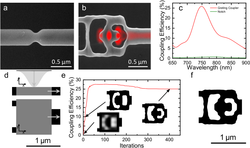
A practical solution to these fabrication and design challenges are notches (Fig. 1a), which are a perturbation to a waveguide with scattering efficiency.Sipahigil2016 In our work, we develop an inverse-designed vertical coupler (Fig. 1b) and use the notch for a baseline comparison. The couplers have a footprint of µm2 and couple directly to a nm wide waveguide without a tapering section, assuring compactness. As shown in Fig. 1c, the simulated peak efficiencies of the coupler (red) and the notch (green) are and ,Sipahigil2016 respectively. Furthermore, we optimize the vertical coupler to couple the light between the fundamental free-space mode and the TE fundamental mode of the waveguide. Even for conventional grating couplers in mature photonics platforms the selective coupling to the mode is a formidable challenge.Laere2007 ; Vermeulen2010 The theoretical maximum coupling efficiency of our couplers is %, because of the symmetry along the z-axis of our devices (i.e. the structure will couple light in +/- z direction equally).
Inverse design problems in photonics are defined by an electromagnetic simulation, a design region and a figure of merit to optimize. The starting conditions of the simulation for vertical couplers are shown in Fig. 1d. A vertically incident Gaussian beam forms the radiative source and is centered above the µm2 design region shown in gray. To the left of the design region are two black support bars to suspend the design, and to the right is a black output waveguide. The fraction of incident light coupled into the fundamental TE mode of the waveguide serves as the figure of merit and is maximized during our optimization process (detailed in reference 38). The coupling efficiency during the optimization is shown in Fig. 1e. At the start of the optimization, any permittivity value between that of air and diamond is allowed, which results in a continuous structure shown in the leftmost inset. After several iterations, this structure is discretized, in which case the permittivity is that of either air or diamond. This discrete structure is further optimized while also gradually imposing a penalty on infabricable features.Lu2013 ; Piggott2017 As a result, the coupling efficiency at a wavelength of nm (silicon-vacancy color center zero-phonon line) peaks at a value of , which then decreases to to comply with fabrication constraints.Piggott2017
Characterization of diamond vertical couplers
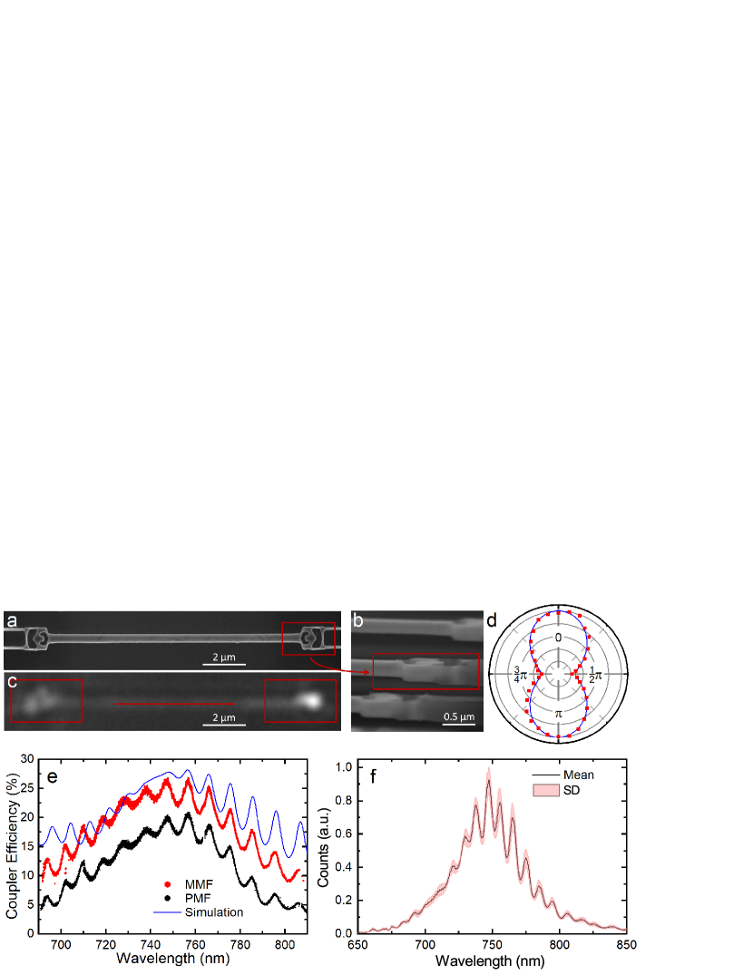
To characterize the coupling efficiency of the vertical couplers, we measure the device shown in Figs. 2a and b, in top-down and side view, respectively. An optical microscope image of the same structure, presented in Fig. 2c, qualitatively shows the high performance of the vertical couplers. We characterize the polarization dependence of the vertical couplers by sweeping the polarization of the input laser beam (Fig. 2d). The observed five-fold reduction in the transmitted power when rotating the polarization by corresponds well to our simulated results (blue line in Fig. 2d) and is experimental evidence for excellent coupling to a linearly polarized mode. In Fig. 2e we present experimentally determined efficiencies of the vertical couplers, which we acquire by coupling a tunable continuous-wave Ti:Sapphire laser to the structures in a cryostat using a NA objective. We then collect the out-coupled beam with a single-mode polarization-maintaining fiber (PMF, black data points) and a multimode fiber (MMF, red data points). The experimental results show peak efficiencies of for PMF and for MMF, with broadband performance of (PMF) and (MMF). The small discrepancy between the measurements with PMF and MMF suggests that we couple very efficiently from the waveguide mode back into the fundamental free-space mode . Moreover, the numerical simulation (blue line) agrees well with the experimental results.
Imposing fabrication constraints, such as minimum feature sizes, on the design optimization guarantees not only high fabrication yield but also robust performance, as we demonstrate in Fig. 2f. Here we overlay transmission spectra of 15 different devices acquired with a supercontinuum source. During the experiments we purposely constrained ourselves to coarse alignment to confirm the robustness to alignment imperfections. The result of our analysis is shown in Fig. 2f, where the solid black line is the mean value of all couplers and the red shaded area indicates the standard deviation at a given wavelength. Moreover, the average efficiency of devices fabricated with various doses is .
Diamond quantum optical interfaces
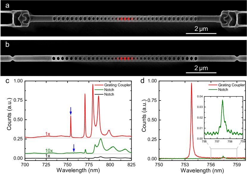
The vertical coupler presented in this work provides a compact, robust, and efficient solution for free-space interfaces in cavity quantum electrodynamics. In particular, our design is optimized to be compatible with simultaneous fabrication of high- resonators for quantum optics experiments, as we avoid additional fabrication stepsLaere2007 ; Vermeulen2010 that could impact the resonator performance. In this section we therefore investigate coupling to the modes of nanophotonic resonators, which are used in quantum optics to enhance light-matter interactionsZhang2018 and to facilitate efficient integration of quantum emitters into optical circuits. We study nanobeam photonic crystal (PhC) cavities, which host a TE mode as shown in Figs. 3a and b. With a supercontinuum light source we acquire the transmission spectra shown in Fig. 3c by coupling a free-space laser beam into the TE fundamental mode of the nanobeam and subsequently into PhC modes. The data in red correspond to the device with vertical couplers, while the black spectrum corresponds to a cavity with notches as the free-space interface for the same input power and integration time. The count rates of the device with notches as an interface are more than two orders of magnitude smaller, for which we compensate by integrating 10 times longer (data in green). When comparing the cavity resonances (blue arrows), we find a -fold increase in counts of the vertical coupler over the notch device for comparable quality factors (). This result matches well with the -fold enhancement that we expect from simulations. This improvement in coupling efficiencies allows for dramatically decreased experimental times (in some cases from weeks to minutes of photon integration), thereby opening opportunities for larger-scale experiments. In Fig. 3d we present spectra, where we couple the laser light directly to the cavity and optimize the alignment to collect maximum counts from the vertical coupler (red) and the notch (green). From this measurement we can conclude that the extraction efficiency of light coupling from the cavity mode to the waveguide is times greater for a vertical coupler than that for a notch, which corresponds well to the transmission experiment.
Inverse-designed diamond photonic circuit
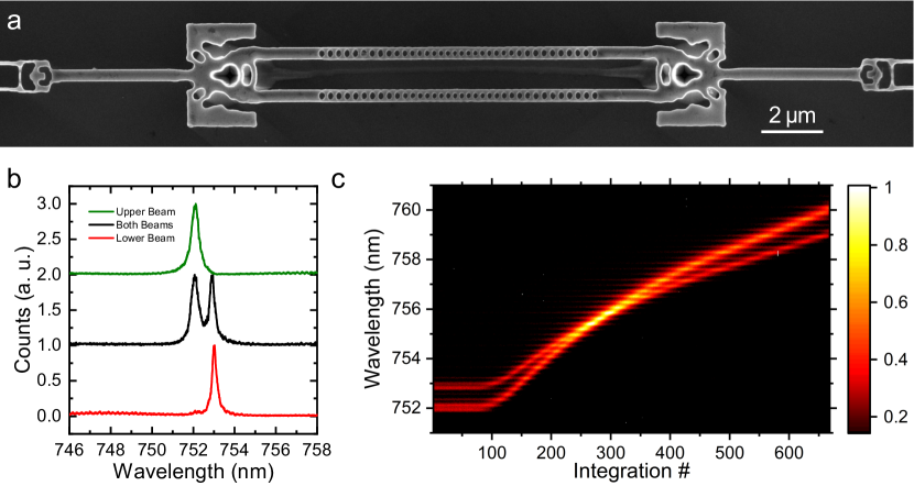
For applications in quantum technologies, many nodes need to be connected to scale from single qubits to large, interconnected qubit arrays.Cirac1997 ; Kimble2008 ; Lemonde2018 This requires the excitation of emitters in multiple cavities, the interference of their emission on beamsplitters, and subsequently the efficient collection and detection of photons. However, up until now elements such as waveguide-splitters have posed a major challenge in suspended diamond photonics, as state-of-the-art fabrication using angled etch is not conducive to variations in the device geometry. In contrast, as shown in Fig. 4a, we can fabricate a conceptual circuit comprised of three components with completely different geometries: vertical couplers, waveguide-splitters, and nanobeam PhC cavities. The device is designed to interfere the transmission of two nanobeam PhC cavities at an inverse-designed waveguide-splitter with a splitting ratio and simulated efficiencies of . We address the cavities separately or simultaneously by top-down excitation with a supercontinuum source focused on the cavities directly, as presented in Fig. 4b. The resonances of the two beams are detuned by nm because of fabrication imperfections. We tune the two cavities into and out of resonance via gas condensation, as shown in Fig. 4c. Comparing the amplitudes of the cavity on and off resonance suggests constructive interference, indicating that the cavities are approximately in phase and have the same polarization. With this concept circuit, we show that inverse design can overcome limitations of classical photonics and enables large-scale on-chip quantum optics experiments. Extending this work we can increase compactness by combining several functionalities into a single device, design circuits for arbitrary emitter locations, assure phase-matching across different paths of the circuits, and optimize for specific bandwidths. Such a platform can then utilize the scalability that diamond color centers offer: site-controlled implantation of high quality color centersEvans2016 ; Schroder2017 and small inhomogeneous broadening,Rogers2014 which can be overcome by cavity-enhanced Raman emissionSipahigil2016 ; Sun2018 or strain tuning.Meesala2016 ; Meesala2018 ; Sohn2018 ; Machielse2019
Highly efficient free-space-waveguide interfaces
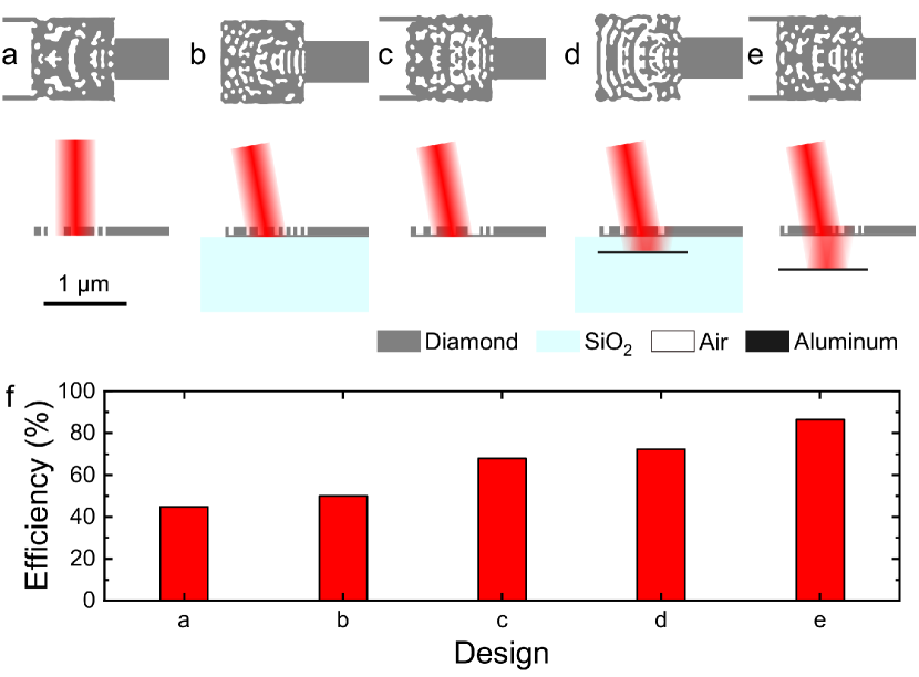
Ultimately the implementation of scalable quantum networks requires efficiencies of building blocks close to unity. Efficiencies of can be achieved with fiber tapers,Burek2017 which have the drawback of significantly larger footprints. To achieve comparable efficiencies, we reduce the fabrication constraints to nm feature sizes, increase the laser spot size, device footprint, and waveguide width. This allows us to improve the simulated efficiency to . However, vertically symmetric devices, such as shown in Fig. 5a cannot exceed efficiency. For further improvements, we tilt the incident laser beam by and break the symmetry along the z-axis of the couplers via a partial etch.Vermeulen2010 In Fig. 5b we show diamond devices on SiO2 with efficiencies of . Such devices could be achieved through diamond thin-film on SiO2 productionHausmann2014 or pick and place techniquesKim2017pickplace and are a promising route for a range of applications including long-distance entanglement schemes, and nonlinear optics. Devices suspended in air (Fig. 5c) have a larger refractive index contrast and show efficiencies of up to . Additionally employing back-reflectorsLaere2007 as shown in Fig. 5d and e results in efficiencies of and , for diamond on SiO2 and suspended structures, respectively. The back-reflector distance to the coupler ( nm and nm) is significantly shorter than the photon wave-packet and optimized to match the phase between reflected and directly coupled photons. These findings are encouraging for the development of highly efficient and compact photonic free-space interfaces as an alternative to fiber tapers for quantum photonic applications at the single-photon level. Moreover, many experiments will require optical driving of individual emitters to compensate for their spectral broadening via Raman processes.Sipahigil2016 ; Sun2018 This individual addressing is easier to implement in free-space coupling configurations than with many tapered fibers inside a cryostat. High efficiencies and compactness will be crucial in these experiments, as losses will be the limiting factor. Thus, inverse design is likely to play a major role in the development of such photonic circuits.Su2018
Discussion
In summary, we employ optimization-based inverse design methods to overcome the constraints of cutting-edge diamond nanofabrication and to develop efficient building blocks for diamond nanophotonic circuits.OBrien2010 In optical free-space couplers and a small diamond photonic circuit we attain the crucial properties of high efficiency, compactness, and robustness. This work now enables more complex quantum circuits, where compact solutions for a variety of device components such as pulse shapers, splitter trees, phase delays,Vampa2017 and mode convertersLu2012 are critical. Thus, this progress lays the foundation for scaling to larger quantum networksCirac1997 ; Kimble2008 ; Wehner2018 with spinsRose2018 embedded in quantum nodes. In addition, inverse design methods can be applied to other promising material platforms that host quantum emitters and have challenging fabrication protocols, such as silicon carbideKoehl2011 and yttrium orthovanadate.Zhong2017
Acknowledgements
We acknowledge the help of Usha Raghuram and Elmer Enriquez with RIE. This work is financially supported by Army Research Office (ARO) (award no. W911NF1310309), Air Force Office of Scientific Research (AFOSR) MURI Center for Attojoule Nano-Optoelectronics (award no. FA9550-17-1-0002), National Science Foundation (NSF) Division Of Electrical, Communications & Cyber Systems (ECCS) (award no. 1838976), and Gordon and Betty Moore Foundation; C.D. acknowledges support from the Andreas Bechtolsheim Stanford Graduate Fellowship and the Microsoft Research PhD Fellowship. K.Y.Y. and M.R. acknowledge support from the Nano- and Quantum Science and Engineering Postdoctoral Fellowship. D.M.L. acknowledges support from the Fong Stanford Graduate Fellowship. D.M.L. and A.E.R. acknowledge support from the National Defense Science and Engineering Graduate (NDSEG) Fellowship Program, sponsored by the Air Force Research Laboratory (AFRL), the Office of Naval Research (ONR) and the Army Research Office (ARO). D.V. acknowledges funding from FWO and European Union’s Horizon 2020 research and innovation program under the Marie Sklodowska-Curie grant agreement No 665501. We thank Google for providing computational resources on the Google Cloud Platform. Part of this work was performed at the Stanford Nanofabrication Facility (SNF) and the Stanford Nano Shared Facilities (SNSF), supported by the National Science Foundation under award ECCS-1542152.
Author contributions C.D. and J.V. conceived and designed the experiment. C.D. developed the fabrication, fabricated the sample and measured and analyzed the data. D.V., N.V.S., C.D. and L.S. conducted inverse design optimization of photonic components. K.Y.Y., D.M.L. and A.Y.P. contributed to the sample fabrication. A.E.R. and S.S. contributed to optical measurements. J.L.Z., M.R. and K.G.L. provided expertise. J.V. supervised the project. All authors participated in the discussion, understanding of the results, and the preparation of the manuscript.
References
- (1) Atatüre, M., Englund, D., Vamivakas, N., Lee, S. Y. & Wrachtrup, J. Material platforms for spin-based photonic quantum technologies. Nat. Mater. 3, 38–51 (2018).
- (2) Awschalom, D. D., Hanson, R., Wrachtrup, J. & Zhou, B. B. Quantum technologies with optically interfaced solid-state spins. Nat. Photonics 12, 516–527 (2018).
- (3) Khanaliloo, B. et al. Single-crystal diamond nanobeam waveguide optomechanics. Phys. Rev. X 5, 041051 (2015).
- (4) Burek, M. J. et al. Diamond optomechanical crystals. Optica 3, 1404–1411 (2015).
- (5) Hausmann, B. J. M., Bulu, I., Venkataraman, V., Deotare, P. & Loncar, M. Diamond nonlinear photonics. Nat. Photonics 8, 369–374 (2014).
- (6) Rose, B. C. et al. Observation of an environmentally insensitive solid-state spin defect in diamond. Science 361, 60–63 (2018).
- (7) Aharonovich, I., Greentree, A. D. & Prawer, S. Diamond photonics. Nat. Photonics 5, 397–405 (2011).
- (8) Cirac, J. I., Zoller, P., Kimble, H. J. & Mabuchi, H. Quantum state transfer and entanglement distribution among distant nodes in a quantum network. Phys. Rev. Lett. 78, 3221 ((1997).
- (9) Briegel, H.-J., Dür, W., Cirac, J. I. & Zoller, P. Quantum repeaters: The role of imperfect local operations in quantum communication. Phys. Rev. Lett. 81, 5932 ((1998).
- (10) Kimble, H. J. The quantum internet. Nature 453, 1023–1030 (2008).
- (11) Bernien, H. et al. Two-photon quantum interference from separate nitrogen vacancy centers in diamond. Phys. Rev. Lett. 108, 043604 (2012).
- (12) Sipahigil, A. et al. Quantum interference of single photons from remote nitrogen-vacancy centers in diamond. Phys. Rev. Lett. 108, 143601 (2012).
- (13) Bernien, H. et al. Heralded entanglement between solid-state qubits separated by three metres. Nature 497, 86–90 (2013).
- (14) Pfaff, W. et al. Unconditional quantum teleportation between distant solid-state quantum bits. Science 345, 532–535 (2014).
- (15) Hensen, B. et al. Loophole-free Bell inequality violation using electron spins separated by 1.3 kilometres. Nature 526, 682–686 (2015).
- (16) Gao, W. B., Imamoglu, A., Bernien, H. & Hanson, R. Coherent manipulation, measurement and entanglement of individual solid-state spins using optical fields. Nat. Photonics 39, 363–373 (2015).
- (17) Sun, S. et al. Cavity-enhanced Raman emission from a single color center in a solid. Phys. Rev. Lett. 121, 083601 (2018).
- (18) Lemonde, M. A. et al. Phonon networks with silicon-vacancy centers in diamond waveguides. Phys. Rev. Lett. 120, 213603 (2018).
- (19) Ladd, T. D. et al. Quantum computers. Nature 464, 45–53 (2010).
- (20) Sipahigil, A. et al. An integrated diamond nanophotonics platform for quantum-optical networks. Science 354, 847–850 (2016).
- (21) Evans, R. E. et al. Photon-mediated interactions between quantum emitters in a diamond nanocavity. Science 362, 662–665 (2018).
- (22) Balasubramanian, G. et al. Nanoscale imaging magnetometry with diamond spins under ambient conditions. Nature 455, 648–651 (2008).
- (23) Degen, C. L., Reinhard, F. & Cappellaro, P. Quantum sensing. Rev. Mod. Phys. 89, 035002 (2017).
- (24) Burek, M. J. et al. High quality-factor optical nanocavities in bulk single-crystal diamond. Nat. Comm. 5, 5718 (2014).
- (25) Khanaliloo, B., Mitchell, M., Hryciw, A. C. & Barclay, P. E. High-Q/V monolithic diamond microdisks fabricated with quasi-isotropic etching. Nano Lett. 15, 5131–5136 (2015).
- (26) Mouradian, S., Wan, N. H., Schröder, T. & Englund, D. Rectangular photonic crystal nanobeam cavities in bulk diamond. Appl. Phys. Lett. 111, 021103 (2017).
- (27) Wan, N. H., Mouradian, S. & Englund, D. Two-dimensional photonic crystal slab nanocavities on bulk single-crystal diamond featured. Appl. Phys. Lett. 112, 141102 (2018).
- (28) Mitchell, M., Lake, D. P. & Barclay, P. E. Realizing q >300 000 in diamond microdisks for optomechanics via etch optimization. APL Photonics 4, 016101 (2019).
- (29) Molesky, S. et al. Inverse design in nanophotonics. Nat. Photonics 12, 659–670 (2018).
- (30) Su, L. et al. Fully-automated optimization of grating couplers. Opt. Express 26, 4023–4034 (2018).
- (31) Van Laere, F. et al. Compact and highly efficient grating couplers between optical fiber and nanophotonic waveguides. J. Light. Technol. 25, 151–156 (2007).
- (32) Vermeulen, D. et al. High-efficiency fiber-to-chip grating couplers realized using an advanced CMOS-compatible silicon-on-insulator platform. Opt. Express 18, 18278–18283 (2010).
- (33) Rath, P., Khasminskaya, S., Nebel, C., Wild, C. & Pernice, W. H. Grating-assisted coupling to nanophotonic circuits in microcrystalline diamond thin films. J. Light. Technol. 4, 300–305 (2013).
- (34) Faraon, A. et al. Quantum photonic devices in single-crystal diamond. New J. Phys. 15, 025010 (2013).
- (35) Piracha, A. H. et al. Scalable fabrication of integrated nanophotonic circuits on arrays of thin single crystal diamond membrane windows. Nano Lett. 16, 3341–3347 (2016).
- (36) Zhou, X. et al. High-Efficiency Shallow-Etched Grating on GaAs Membranes for Quantum Photonic Applications. Appl. Phys. Lett. 113, 251103 (2018).
- (37) Gould, M., Schmidgall, E. R., Dadgostar, S., Hatami, F. & Fu, K.-M. C. Efficient extraction of zero-phonon-line photons from single nitrogen-vacancy centers in an integrated gap-on-diamond platform. Phys. Rev. Applied 6, 011001 (2016).
- (38) Piggott, A. Y. et al. Inverse design and implementation of a wavelength demultiplexing grating coupler. Sci. Rep. 4, 7210 (2014).
- (39) Lu, J. & Vuckovic, J. Nanophotonic computational design. Opt. Express 21, 13351–13367 (2013).
- (40) Piggott, A. Y., Petykiewicz, J., Su, L. & Vučković, J. Fabrication-constrained nanophotonic inverse design. Sci. Rep. 7, 1786 (2017).
- (41) Zhang, J. L. et al. Strongly cavity-enhanced spontaneous emission from silicon-vacancy centers in diamond. Nano Lett. 18, 1360–1365 (2018).
- (42) Evans, R. E., Sipahigil, A., Sukachev, D. D., Zibrov, A. S. & Lukin, M. D. Narrow-linewidth homogeneous optical emitters in diamond nanostructures via silicon ion implantation. Phys. Rev. Applied 5, 044010 (2016).
- (43) Schröder, T. et al. Scalable focused ion beam creation of nearly lifetime-limited single quantum emitters in diamond nanostructures. Nat. Commun. 8, 15376 (2017).
- (44) Rogers, L. et al. Multiple intrinsically identical single-photon emitters in the solid state. Nat. Commun. 5, 4739 (2014).
- (45) Meesala, S. et al. Enhanced strain coupling of nitrogen-vacancy spins to nanoscale diamond cantilevers. Phys. Rev. Appl. 5, 034010 (2016).
- (46) Meesala, S. et al. Strain engineering of the silicon-vacancy center in diamond. Phys. Rev. B 97, 205444 (2018).
- (47) Sohn, Y.-I. et al. Controlling the coherence of a diamond spin qubit through its strain environment. Nat. Commun. 9, 2012 (2018).
- (48) Machielse, B. et al. Quantum interference of electromechanically stabilized emitters in nanophotonic devices. preprint at http://arXiv.org/abs/1901.09103 (2019).
- (49) Burek, M. J. et al. Fiber-coupled diamond quantum nanophotonic interface. Phys. Rev. Applied 8, 024026 (2017).
- (50) Kim, J.-H. et al. Hybrid integration of solid-state quantum emitters on a silicon photonic chip. Nano Lett. 17, 7394–7400 (2017).
- (51) O’Brien, J. L., Furusawa, A. & Vučković, J. Photonic quantum technologies. Nat. Photonics 3, 687–695 (2009).
- (52) Vampa, G., Fattahi, H., Vuckovic, J. & Krausz, F. Attosecond nanophotonics. Nat. Photonics 11, 210–212 (2017).
- (53) Lu, J. & Vučković, J. Objective-first design of high-efficiency, small-footprint couplers between arbitrary nanophotonic waveguide modes. Opt. Express 20, 7221–7236 (2012).
- (54) Wehner, S., Elkouss, D. & Hanson, R. Quantum internet: A vision for the road ahead. Science 362, 6412 (2018).
- (55) Koehl, W. F., Buckley, B. B., Heremans, F. J., Calusine, G. & Awschalom, D. D. Room temperature coherent control of defect spin qubits in silicon carbide. Nature 479, 84–87 (2011).
- (56) Zhong, T. et al. Nanophotonic rare-earth quantum memory with optically controlled retrieval. Science 357, 1392–1395 (2017).